EP0903859A2 - Diviseur de fréquence à faible consommation - Google Patents
Diviseur de fréquence à faible consommation Download PDFInfo
- Publication number
- EP0903859A2 EP0903859A2 EP98116970A EP98116970A EP0903859A2 EP 0903859 A2 EP0903859 A2 EP 0903859A2 EP 98116970 A EP98116970 A EP 98116970A EP 98116970 A EP98116970 A EP 98116970A EP 0903859 A2 EP0903859 A2 EP 0903859A2
- Authority
- EP
- European Patent Office
- Prior art keywords
- divider
- signal
- frequency
- input
- output
- Prior art date
- Legal status (The legal status is an assumption and is not a legal conclusion. Google has not performed a legal analysis and makes no representation as to the accuracy of the status listed.)
- Granted
Links
Images

Classifications
-
- H—ELECTRICITY
- H03—ELECTRONIC CIRCUITRY
- H03K—PULSE TECHNIQUE
- H03K23/00—Pulse counters comprising counting chains; Frequency dividers comprising counting chains
- H03K23/64—Pulse counters comprising counting chains; Frequency dividers comprising counting chains with a base or radix other than a power of two
- H03K23/66—Pulse counters comprising counting chains; Frequency dividers comprising counting chains with a base or radix other than a power of two with a variable counting base, e.g. by presetting or by adding or suppressing pulses
- H03K23/667—Pulse counters comprising counting chains; Frequency dividers comprising counting chains with a base or radix other than a power of two with a variable counting base, e.g. by presetting or by adding or suppressing pulses by switching the base during a counting cycle
Definitions
- frequency divider is intended to include so-called Dual modulus prescaler "can be understood, as they are used in frequency synthesizers of mobile telecommunication systems.
- Such frequency dividers have switchable division factors between 1 / N and 1 / (N + 1), where N is typically 64 or 128, and operate with frequencies of the order of magnitude of 1 GHz and are part of every GSM or DECT telephone. Because of the usually available battery supply of the devices, a low power consumption is of essential importance.
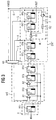
- FIG. 1 shows an example of a frequency divider for the division factors 1/64 and 1/65, this having an input-side frequency halve H, an intermediate divider 4/5 and a divider extension EXT.
- the input-side frequency bisector H generates from an input signal IN with the frequency f an intermediate signal 1 which only has the frequency f / 2.
- a second intermediate signal 2 with the frequency f / 8 is obtained from the first intermediate signal by reducing the frequency with the division factor 1/4 and in the case of a desired division factor 1 / (N + 1) generates the intermediate signal 2 with the frequency f / 10 from the first intermediate signal by reducing the frequency with the division factor 1/5.
- the divider extension EXT has 2 N-2 divider stages (FF5 ... FF8), the penultimate divider stage FF7 of which provides an output signal OUT with the frequency f / N or f / (N + 1).
- the switchover signal U is formed by an AND gate A3 from a negated control signal MOD and from the negated output signals 3 ... 6 of the divider stages FF5 ... FF8.
- the frequency bisector is designed here such that the input signal IN of the frequency divider serves as a clock signal for a D flip-flop FF1, the inverted input of which carries signal 1 and is fed back to the D input.
- the intermediate divider 4/5 contains three flip-flops FF2 ...
- flip-flop FF4 synchronously clocked by the signal 1, the D input of the flip-flop FF2 being connected to an AND gate A1, which combines the switchover signal U with the second signal 2, the D input of flip-flop FF3 is connected to an AND gate A2, which links a negated output signal of flip-flop FF2 with a negated output signal of flip-flop FF4, and the non-inverted output of flip-flop FF3 is connected to the D input of flip-flop FF4 .
- the flip-flops FF5 ... FF8 of the divider extension EXT are connected here as an asynchronous counter, the clock input of the D-flip-flops FF6 ...
- All flip-flops FF1 ... FF8 are D-flip-flops with a clock input triggering on positive signal edges.
- the frequency halving on the input side results in a division by 128 or 130 at the output of the last stage of the extension divider EXT.
- the output signal OUT is that shown in Figure 1 Circuit shown, the output signal such is that after 34 periods of high level, 32 periods with low level, then again 32 periods high level and finally 32 low-level periods occur again.
- This signal shows next to the desired fundamental wave another signal of half the output frequency and the Amplitude 2/65. This corresponds to an undesired overlay an interference voltage (jitter) with the frequency of the fundamental wave of the output signal.
- FIG. 3 another preferred embodiment of the invention specified in the case of a modified divider extension EXT 'with a jitter compensation device JK a jitter is avoided at the output OUT.
- the circuit of Figure 3 corresponds except for the modified part extension EXT 'instead the divider extension EXT of the circuit of FIG. 2.
- the jitter compensation device JK exists here, for example in that the inverted output signal 4 of the flip-flop FF6 through a resistor R1 to the clock input of the Flip-flop FF7 is connected and the clock input of the flip-flop A signal 7 is fed to FF7 via a further resistor R2 is that by an AND operation (A4) of the inverted Output signal of the flip-flop FF8 and the inverted control signal MOD is formed.
- This causes the Signal 4 a signal with the amplitude - 2/65 with half Frequency of the output signal admixed and thereby the jitter is eliminated.
- JK Jitter compensation device
Landscapes
- Stabilization Of Oscillater, Synchronisation, Frequency Synthesizers (AREA)
- Manipulation Of Pulses (AREA)
Applications Claiming Priority (2)
| Application Number | Priority Date | Filing Date | Title |
|---|---|---|---|
| DE19741210 | 1997-09-18 | ||
| DE19741210 | 1997-09-18 |
Publications (3)
| Publication Number | Publication Date |
|---|---|
| EP0903859A2 true EP0903859A2 (fr) | 1999-03-24 |
| EP0903859A3 EP0903859A3 (fr) | 1999-12-15 |
| EP0903859B1 EP0903859B1 (fr) | 2004-11-24 |
Family
ID=7842840
Family Applications (1)
| Application Number | Title | Priority Date | Filing Date |
|---|---|---|---|
| EP98116970A Expired - Lifetime EP0903859B1 (fr) | 1997-09-18 | 1998-09-08 | Diviseur de fréquence à faible consommation |
Country Status (4)
| Country | Link |
|---|---|
| US (1) | US6067339A (fr) |
| EP (1) | EP0903859B1 (fr) |
| JP (1) | JP3571228B2 (fr) |
| DE (1) | DE59812296D1 (fr) |
Cited By (1)
| Publication number | Priority date | Publication date | Assignee | Title |
|---|---|---|---|---|
| WO2007085867A1 (fr) * | 2006-01-24 | 2007-08-02 | Future Waves Uk Limited | Circuits diviseurs de frequence |
Families Citing this family (11)
| Publication number | Priority date | Publication date | Assignee | Title |
|---|---|---|---|---|
| FR2769432B1 (fr) * | 1997-10-03 | 2000-01-28 | Thomson Csf | Diviseur de frequence a modulo variable |
| US6873743B2 (en) * | 2001-03-29 | 2005-03-29 | Fotonation Holdings, Llc | Method and apparatus for the automatic real-time detection and correction of red-eye defects in batches of digital images or in handheld appliances |
| US6751348B2 (en) * | 2001-03-29 | 2004-06-15 | Fotonation Holdings, Llc | Automated detection of pornographic images |
| EP1300950A1 (fr) * | 2001-10-05 | 2003-04-09 | Asulab S.A. | Circuit compteur diviseur double mode à phase commutée pour un synthétiseur de fréquence |
| US6760398B2 (en) * | 2001-10-05 | 2004-07-06 | Asulab S.A. | Switched phase dual-modulus prescaler circuit having means for reducing power consumption |
| US6696857B1 (en) | 2003-01-07 | 2004-02-24 | Institute Of Microelectronics | High speed CMOS dual modulus prescaler using pull down transistor |
| JP4077483B2 (ja) * | 2003-05-20 | 2008-04-16 | 日本電信電話株式会社 | 可変分周方法および可変分周器 |
| US6967507B2 (en) * | 2004-01-15 | 2005-11-22 | Agilent Technologies, Inc. | Dual edge count programmable frequency divider |
| US7486145B2 (en) * | 2007-01-10 | 2009-02-03 | International Business Machines Corporation | Circuits and methods for implementing sub-integer-N frequency dividers using phase rotators |
| CN104113325B (zh) * | 2013-04-19 | 2018-09-28 | 南京中兴软件有限责任公司 | 一种多模可编程分频器 |
| US9679194B2 (en) | 2014-07-17 | 2017-06-13 | At&T Intellectual Property I, L.P. | Automated obscurity for pervasive imaging |
Family Cites Families (8)
| Publication number | Priority date | Publication date | Assignee | Title |
|---|---|---|---|---|
| JPS59181831A (ja) * | 1983-03-31 | 1984-10-16 | Toshiba Corp | 可変分周器 |
| DE3503182A1 (de) * | 1985-01-31 | 1986-08-07 | Deutsche Thomson-Brandt Gmbh, 7730 Villingen-Schwenningen | Programmierbarer zaehler |
| JPS63151217A (ja) * | 1986-12-16 | 1988-06-23 | Fujitsu Ltd | 歯抜け分周回路 |
| JPH034618A (ja) * | 1989-05-31 | 1991-01-10 | Nec Eng Ltd | クロック分周回路 |
| JPH0548433A (ja) * | 1991-08-16 | 1993-02-26 | Nippon Telegr & Teleph Corp <Ntt> | 多段分周器 |
| JPH0590953A (ja) * | 1991-09-30 | 1993-04-09 | Fujitsu Ltd | 半導体論理回路 |
| JPH0645913A (ja) * | 1992-07-24 | 1994-02-18 | Nec Corp | クロック分周回路 |
| JPH07221633A (ja) * | 1994-01-28 | 1995-08-18 | Fujitsu Ltd | 2モジュラスプリスケーラ |
-
1998
- 1998-09-08 DE DE59812296T patent/DE59812296D1/de not_active Expired - Fee Related
- 1998-09-08 EP EP98116970A patent/EP0903859B1/fr not_active Expired - Lifetime
- 1998-09-15 US US09/153,060 patent/US6067339A/en not_active Expired - Fee Related
- 1998-09-18 JP JP26493698A patent/JP3571228B2/ja not_active Expired - Fee Related
Cited By (2)
| Publication number | Priority date | Publication date | Assignee | Title |
|---|---|---|---|---|
| WO2007085867A1 (fr) * | 2006-01-24 | 2007-08-02 | Future Waves Uk Limited | Circuits diviseurs de frequence |
| US7808287B2 (en) | 2006-01-24 | 2010-10-05 | Future Waves Uk Limited | Frequency divider circuits |
Also Published As
| Publication number | Publication date |
|---|---|
| JPH11186900A (ja) | 1999-07-09 |
| EP0903859B1 (fr) | 2004-11-24 |
| EP0903859A3 (fr) | 1999-12-15 |
| JP3571228B2 (ja) | 2004-09-29 |
| US6067339A (en) | 2000-05-23 |
| DE59812296D1 (de) | 2004-12-30 |
Similar Documents
| Publication | Publication Date | Title |
|---|---|---|
| DE60224478T2 (de) | Schaltung zur Serialisierung von synchronen Daten | |
| DE69100204T2 (de) | Einrichtung zur Erzeugung von Testsignalen. | |
| DE69027152T2 (de) | Hoch-Resolutionsabtast-Taktgenerator mit Deglitcher-Anordnung | |
| DE69227608T2 (de) | Veränderliche Taktteilerschaltung | |
| DE3850793T2 (de) | Phasenkomparatorschaltung. | |
| DE69502071T2 (de) | Einstellbare Verzögerungsschaltung | |
| DE19917320A1 (de) | Taktgenerator für ein Halbleiter-Prüfsystem | |
| DE2625545A1 (de) | Automatische taktimpuls-abgleichvorrichtung | |
| EP0903859B1 (fr) | Diviseur de fréquence à faible consommation | |
| DE68926518T2 (de) | Flipflop-Schaltung | |
| DE69100176T2 (de) | Impulsformerschaltung. | |
| DE3022746A1 (de) | Digitale phasenkomparatorschaltung | |
| DE10251703B4 (de) | Schaltungsanordnung zur Frequenzteilung und Phasenregelschleife mit der Schaltungsanordnung | |
| DE4306463C2 (de) | System zur Erzeugung von Datensignalen zur Anlegung an ein in Prüfung befindliches Gerät mit unabhängig voneinander einstellbaren steigenden und fallenden Flanken | |
| DE3743586C2 (fr) | ||
| DE69426361T2 (de) | Digital-analog-umsetzer mit symmetrischem differentialschalter | |
| DE69511628T2 (de) | Pulserzeugung | |
| DE69128509T2 (de) | Zeitgeber | |
| DE60307150T2 (de) | Verfahren und Vorrichtung zur statistischen Signalverlustdetektion bei geringer kapazitiver Belastung der Eingangssignale | |
| DE19811591C2 (de) | Taktsignal modellierende Schaltung mit negativer Verzögerung | |
| EP0903858B1 (fr) | Diviseur de fréquence à faible consommation | |
| DE102005051770A1 (de) | Verfahren und Vorrichtung zum Umschalten der Frequenz eines Systemtakts | |
| DE68925799T2 (de) | Einen metastabilen Zustand zulassende Kippschaltung | |
| EP1094610A1 (fr) | Boucle de verrouillage de phase numérique | |
| EP0150325B1 (fr) | Unité de retard pour l'obtention d'un signal de sortie retardé |
Legal Events
| Date | Code | Title | Description |
|---|---|---|---|
| PUAI | Public reference made under article 153(3) epc to a published international application that has entered the european phase |
Free format text: ORIGINAL CODE: 0009012 |
|
| AK | Designated contracting states |
Kind code of ref document: A2 Designated state(s): DE FR GB |
|
| AX | Request for extension of the european patent |
Free format text: AL;LT;LV;MK;RO;SI |
|
| PUAL | Search report despatched |
Free format text: ORIGINAL CODE: 0009013 |
|
| AK | Designated contracting states |
Kind code of ref document: A3 Designated state(s): AT BE CH CY DE DK ES FI FR GB GR IE IT LI LU MC NL PT SE |
|
| AX | Request for extension of the european patent |
Free format text: AL;LT;LV;MK;RO;SI |
|
| RIC1 | Information provided on ipc code assigned before grant |
Free format text: 6H 03K 23/66 A, 6H 03K 23/58 B |
|
| 17P | Request for examination filed |
Effective date: 20000121 |
|
| AKX | Designation fees paid |
Free format text: DE FR GB |
|
| RAP1 | Party data changed (applicant data changed or rights of an application transferred) |
Owner name: INFINEON TECHNOLOGIES AG |
|
| 17Q | First examination report despatched |
Effective date: 20021024 |
|
| GRAP | Despatch of communication of intention to grant a patent |
Free format text: ORIGINAL CODE: EPIDOSNIGR1 |
|
| GRAS | Grant fee paid |
Free format text: ORIGINAL CODE: EPIDOSNIGR3 |
|
| GRAA | (expected) grant |
Free format text: ORIGINAL CODE: 0009210 |
|
| AK | Designated contracting states |
Kind code of ref document: B1 Designated state(s): DE FR GB |
|
| PG25 | Lapsed in a contracting state [announced via postgrant information from national office to epo] |
Ref country code: GB Free format text: LAPSE BECAUSE OF FAILURE TO SUBMIT A TRANSLATION OF THE DESCRIPTION OR TO PAY THE FEE WITHIN THE PRESCRIBED TIME-LIMIT Effective date: 20041124 Ref country code: FR Free format text: LAPSE BECAUSE OF NON-PAYMENT OF DUE FEES Effective date: 20041124 |
|
| REG | Reference to a national code |
Ref country code: GB Ref legal event code: FG4D Free format text: NOT ENGLISH |
|
| REF | Corresponds to: |
Ref document number: 59812296 Country of ref document: DE Date of ref document: 20041230 Kind code of ref document: P |
|
| GBV | Gb: ep patent (uk) treated as always having been void in accordance with gb section 77(7)/1977 [no translation filed] |
Effective date: 20041124 |
|
| PLBE | No opposition filed within time limit |
Free format text: ORIGINAL CODE: 0009261 |
|
| STAA | Information on the status of an ep patent application or granted ep patent |
Free format text: STATUS: NO OPPOSITION FILED WITHIN TIME LIMIT |
|
| 26N | No opposition filed |
Effective date: 20050825 |
|
| EN | Fr: translation not filed | ||
| PGFP | Annual fee paid to national office [announced via postgrant information from national office to epo] |
Ref country code: DE Payment date: 20061114 Year of fee payment: 9 |
|
| PG25 | Lapsed in a contracting state [announced via postgrant information from national office to epo] |
Ref country code: DE Free format text: LAPSE BECAUSE OF NON-PAYMENT OF DUE FEES Effective date: 20080401 |