EP0903859A2 - Low-consumption frequency divider - Google Patents
Low-consumption frequency divider Download PDFInfo
- Publication number
- EP0903859A2 EP0903859A2 EP98116970A EP98116970A EP0903859A2 EP 0903859 A2 EP0903859 A2 EP 0903859A2 EP 98116970 A EP98116970 A EP 98116970A EP 98116970 A EP98116970 A EP 98116970A EP 0903859 A2 EP0903859 A2 EP 0903859A2
- Authority
- EP
- European Patent Office
- Prior art keywords
- divider
- signal
- frequency
- input
- output
- Prior art date
- Legal status (The legal status is an assumption and is not a legal conclusion. Google has not performed a legal analysis and makes no representation as to the accuracy of the status listed.)
- Granted
Links
Images

Classifications
-
- H—ELECTRICITY
- H03—ELECTRONIC CIRCUITRY
- H03K—PULSE TECHNIQUE
- H03K23/00—Pulse counters comprising counting chains; Frequency dividers comprising counting chains
- H03K23/64—Pulse counters comprising counting chains; Frequency dividers comprising counting chains with a base or radix other than a power of two
- H03K23/66—Pulse counters comprising counting chains; Frequency dividers comprising counting chains with a base or radix other than a power of two with a variable counting base, e.g. by presetting or by adding or suppressing pulses
- H03K23/667—Pulse counters comprising counting chains; Frequency dividers comprising counting chains with a base or radix other than a power of two with a variable counting base, e.g. by presetting or by adding or suppressing pulses by switching the base during a counting cycle
Definitions
- frequency divider is intended to include so-called Dual modulus prescaler "can be understood, as they are used in frequency synthesizers of mobile telecommunication systems.
- Such frequency dividers have switchable division factors between 1 / N and 1 / (N + 1), where N is typically 64 or 128, and operate with frequencies of the order of magnitude of 1 GHz and are part of every GSM or DECT telephone. Because of the usually available battery supply of the devices, a low power consumption is of essential importance.
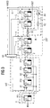
- FIG. 1 shows an example of a frequency divider for the division factors 1/64 and 1/65, this having an input-side frequency halve H, an intermediate divider 4/5 and a divider extension EXT.
- the input-side frequency bisector H generates from an input signal IN with the frequency f an intermediate signal 1 which only has the frequency f / 2.
- a second intermediate signal 2 with the frequency f / 8 is obtained from the first intermediate signal by reducing the frequency with the division factor 1/4 and in the case of a desired division factor 1 / (N + 1) generates the intermediate signal 2 with the frequency f / 10 from the first intermediate signal by reducing the frequency with the division factor 1/5.
- the divider extension EXT has 2 N-2 divider stages (FF5 ... FF8), the penultimate divider stage FF7 of which provides an output signal OUT with the frequency f / N or f / (N + 1).
- the switchover signal U is formed by an AND gate A3 from a negated control signal MOD and from the negated output signals 3 ... 6 of the divider stages FF5 ... FF8.
- the frequency bisector is designed here such that the input signal IN of the frequency divider serves as a clock signal for a D flip-flop FF1, the inverted input of which carries signal 1 and is fed back to the D input.
- the intermediate divider 4/5 contains three flip-flops FF2 ...
- flip-flop FF4 synchronously clocked by the signal 1, the D input of the flip-flop FF2 being connected to an AND gate A1, which combines the switchover signal U with the second signal 2, the D input of flip-flop FF3 is connected to an AND gate A2, which links a negated output signal of flip-flop FF2 with a negated output signal of flip-flop FF4, and the non-inverted output of flip-flop FF3 is connected to the D input of flip-flop FF4 .
- the flip-flops FF5 ... FF8 of the divider extension EXT are connected here as an asynchronous counter, the clock input of the D-flip-flops FF6 ...
- All flip-flops FF1 ... FF8 are D-flip-flops with a clock input triggering on positive signal edges.
- the frequency halving on the input side results in a division by 128 or 130 at the output of the last stage of the extension divider EXT.
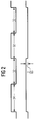
- the output signal OUT is that shown in Figure 1 Circuit shown, the output signal such is that after 34 periods of high level, 32 periods with low level, then again 32 periods high level and finally 32 low-level periods occur again.
- This signal shows next to the desired fundamental wave another signal of half the output frequency and the Amplitude 2/65. This corresponds to an undesired overlay an interference voltage (jitter) with the frequency of the fundamental wave of the output signal.
- FIG. 3 another preferred embodiment of the invention specified in the case of a modified divider extension EXT 'with a jitter compensation device JK a jitter is avoided at the output OUT.
- the circuit of Figure 3 corresponds except for the modified part extension EXT 'instead the divider extension EXT of the circuit of FIG. 2.
- the jitter compensation device JK exists here, for example in that the inverted output signal 4 of the flip-flop FF6 through a resistor R1 to the clock input of the Flip-flop FF7 is connected and the clock input of the flip-flop A signal 7 is fed to FF7 via a further resistor R2 is that by an AND operation (A4) of the inverted Output signal of the flip-flop FF8 and the inverted control signal MOD is formed.
- This causes the Signal 4 a signal with the amplitude - 2/65 with half Frequency of the output signal admixed and thereby the jitter is eliminated.
- JK Jitter compensation device
Landscapes
- Stabilization Of Oscillater, Synchronisation, Frequency Synthesizers (AREA)
- Manipulation Of Pulses (AREA)
Abstract
Description
Unter dem Begriff Frequenzteiler sollen hier insbesondere sogenannte

Beispiele für die Verwendung und den Aufbau solcher Prescaler sind aus dem IEEE Journal of Solid-State Circuits, Vol. 29, No. 10, Oct. 1994, pp. 1206 bis 1211 sowie Vol. 27, No. 12, Dec. 1992, pp. 1794 bis 1798, bekannt, wobei jeweils einem synchronen 1:4/5-Teiler weitere asynchrone Teilererweiterungsstufen nachgeschaltet sind.Examples of the use and structure of such prescaler are from the IEEE Journal of Solid-State Circuits, Vol. 29, No. 10, Oct. 1994, pp. 1206 to 1211 and vol. 27, no. 12, December 1992, pp. 1794 to 1798, known, one each synchronous 1: 4/5 divider further asynchronous divider expansion levels are connected downstream.
Die der Erfindung zugrundeliegende Aufgabe besteht nun darin, einen Frequenzteiler der oben angegebenen Art anzugeben, der einen besonders geringen Stromverbrauch aufweist. Diese Aufgabe wird anhand der Merkmale des Patentanspruchs 1 gelöst. Die weiteren Patentansprüche betreffen eine vorteilhafte Ausgestaltung der Erfindung.The object on which the invention is based is now specify a frequency divider of the type specified above, the has a particularly low power consumption. This task is solved based on the features of claim 1. The other claims relate to an advantageous Embodiment of the invention.
Im folgenden wird anhand der Zeichnung ein bevorzugtes Ausführungsbeispiel der Erfindung näher erläutert. Dabei zeigt
- Figur 1
- ein Schaltbild eines bevorzugten Ausführungsbeispiels und
Figur 2- Zeitdiagramme zur Erläuterung der Funktionsweise der Schaltung nach Figur 1 und
Figur 3- ein Schaltbild eines weiteren bevorzugten Ausführungsbeispiels.
- Figure 1
- a circuit diagram of a preferred embodiment and
- Figure 2
- Time diagrams to explain the operation of the circuit of Figure 1 and
- Figure 3
- a circuit diagram of another preferred embodiment.
Bei der Erfindung wird zunächst aus dem Eingangssignal IN mit
der Frequenz f durch einen Frequenzhalbierer ein Zwischensignal
mit der Frequenz f/2 gebildet, bevor dieses Signal, wie
beim Stand der Technik, einem 1:4/5-Teiler zugeführt wird.
Ferner wird das Ausgangssignal an Stelle einer letzten Stufe
einer vorletzten Stufe eines Erweiterungsteilers als Ausgangssignal
des Frequenzteilers verwendet. Dies hat zur Folge,
daß nur ein Flipflop mit der maximalen Frequenz f = 1 GHz
betrieben wird und somit eine deutliche Senkung des Gesamtstromverbrauches
des Frequenzteilers erreicht werden
kann. Da unter Umständen hierbei auf einen Vorverstärker zum
Treiben der Taktleitungen des Zwischenteilers 4/5 verzichtet
werden kann, führt dies zu einer weiteren Stromreduzierung.In the invention, the input signal IN is first used
the frequency f an intermediate signal by a frequency bisector
formed with the frequency f / 2 before this signal, like
in the prior art, a 1: 4/5 divider is supplied.
Furthermore, the output signal is in place of a last stage
a penultimate stage of an expansion divider as an output signal
of the frequency divider used. As a consequence,
that only a flip-flop with the maximum frequency f = 1 GHz
is operated and thus a significant reduction in total electricity consumption
of the frequency divider can be achieved
can. Under certain circumstances, because of a preamplifier
Driving the clock lines of the
In Figur 1 ist beispielhaft ein Frequenzteiler für die Teilungsfaktoren
1/64 und 1/65 gezeigt, wobei dieser einen eingangsseitigen
Frequenshalbierer H, einen Zwischenteiler 4/5
und eine Teilererweiterung EXT aufweist. Der eingangsseitige
Frequenzhalbierer H erzeugt aus einem Eingangssignal IN mit
der Frequenz f ein Zwischensignal 1, das lediglich die Frequenz
f/2 aufweist. Im Zwischenteiler 4/5 wird abhängig von
einem Umschaltsignal U, im Falle eines gewünschten Teilungsfaktors
1/N ein zweites Zwischensignal 2 mit der Frequenz f/8
aus dem ersten Zwischensignal durch Herabsetzen der Frequenz
mit dem Teilungsfaktor 1/4 und im Falle eines gewünschten
Teilerungsfaktors 1/(N+1) das Zwischensignal 2 mit der Frequenz
f/10 aus dem ersten Zwischensignal durch Herabsetzen
der Frequenz mit dem Teilungsfaktor 1/5 erzeugt. Die Teilererweiterung
EXT weist 2N-2 Teilerstufen (FF5 ... FF8) auf,
deren vorletzte Teilerstufe FF7 ein Ausgangssignal OUT mit
der Frequenz f/N bzw. f/(N + 1) liefert. Das Umschaltsignal U
wird durch ein UND-Gatter A3 aus einem negierten Steuersignal
MOD und aus den negierten Ausgangssignalen 3 ... 6 der Teilerstufen
FF5 ... FF8 gebildet. Der Frequenzhalbierer ist
hier derart ausgebildet, daß das Eingangssignal IN des Frequenzteilers
als Taktsignal für ein D-Flipflop FF1 dient,
dessen invertierter Eingang das Signal 1 führt und auf den D-Eingang
rückgekoppelt ist. Der Zwischenteiler 4/5 enthält
drei durch das Signal 1 synchron getaktete Flipflops FF2 ...
FF4, wobei der D-Eingang des Flipflops FF2 mit einem UND-Gatter
A1 verbunden ist, das das Umschaltsignal U mit dem
zweiten Signal 2 verknüpft, wobei der D-Eingang des Flipflops
FF3 mit einem UND-Gatter A2 verbunden ist, das ein negiertes
Ausgangssignal des Flipflops FF2 mit einem negierten Ausgangssignal
des Flipflops FF4 verknüpft, und wobei der nicht
invertierte Ausgang des Flipflops FF3 mit dem D-Eingang des
Flipflops FF4 verbunden ist. Die Flipflops FF5 ... FF8 der
Teilererweiterung EXT sind hier als asynchroner Zähler geschaltet,
wobei der Takteingang der D-Flipflops FF6 ... FF8
jeweils mit dem invertierten Ausgang der Vorgängenstufe verbunden
ist und der Takteingang des Flipflops FF5 das Signal 2
erhält. Alle Flipflops FF1 ... FF8 sind D-Flipflops mit einem
auf positive Signalflanken triggernden Takteingang.
Durch die eingangsseitige Frequenzhalbierung entsteht am Ausgang
der letzten Stufe des Erweiterungsteilers EXT eine Teilung
durch 128 bzw. 130. Durch das Abgreifen des Ausgangssignals
OUT am Ausgang der vorletzten Stufe des Erweiterungsteilers
wird die gewünschte Teilung durch 64 bzw. 65 erreicht.FIG. 1 shows an example of a frequency divider for the division factors 1/64 and 1/65, this having an input-side frequency halve H, an
In Figur 2 ist das Ausgangssignal OUT der in Figur 1 gezeigten
Schaltung dargestellt, wobei das Ausgangssignal dergestalt
ist, daß nach 34 Perioden mit High-Pegel, 32 Perioden
mit Low-Pegel, dann wieder 32 Perioden High-Pegel und
schließlich wieder 32 Perioden Low-Pegel auftreten. Eine Analyse
dieses Signals zeigt neben der gewünschten Grundwelle
ein weiteres Signal der halben Ausgangsfrequenz und der
Amplitude 2/65. Dies entspricht einer unerwünschten Überlagerung
einer Störspannung (Jitter) mit der Frequenz der Grundwelle
des Ausgangssignals.In Figure 2, the output signal OUT is that shown in Figure 1
Circuit shown, the output signal such
is that after 34 periods of high level, 32 periods
with low level, then again 32 periods high level and
finally 32 low-level periods occur again. An analysis
this signal shows next to the desired fundamental wave
another signal of half the output frequency and the
Zur Beseitigung dieses unerwünschten Jitters ist in Figur 3
ein weiteres bevorzugtes Ausführungsbeispiel der Erfindung
angegeben, bei dem durch eine modifizierte Teilererweiterung
EXT' mit einer Jitterkompensationseinrichtung JK ein Jitter
am Ausgang OUT vermieden wird. Die Schaltung von Figur 3 entspricht
bis auf die modifizierte Teilererweiterung EXT' anstelle
der Teilererweiterung EXT der Schaltung von Figur 2.
Die Jitterkompenstionseinrichtung JK besteht hier beispielsweise
darin, daß das invertierte Ausgangssignal 4 des Flipflops
FF6 über einen Widerstand R1 mit dem Takteingang des
Flipflops FF7 verbunden ist und dem Takteingang des Flipflops
FF7 über einen weiteren Widerstand R2 ein Signal 7 zugeführt
wird, das durch eine UND-Verknüpfung (A4) des invertierten
Ausgangssignals des Flipflops FF8 und des invertierten Steuersignals
MOD gebildet wird. Hierdurch wird bewirkt, daß dem
Signal 4 ein Signal mit der Amplitude - 2/65 mit der halben
Frequenz des Ausgangssignals zugemischt und dadurch der Jitter
beseitigt wird.To eliminate this unwanted jitter is shown in Figure 3
another preferred embodiment of the invention
specified in the case of a modified divider extension
EXT 'with a jitter compensation device JK a jitter
is avoided at the output OUT. The circuit of Figure 3 corresponds
except for the modified part extension EXT 'instead
the divider extension EXT of the circuit of FIG. 2.
The jitter compensation device JK exists here, for example
in that the inverted
Bei einer geraden Anzahl von Teilererweiterungsstufen ist die Jitterkompensationseinrichtung (JK) allgeinen derart aufgebaut, daß nach der ersten Hälfte der Teilerstufen (FF5, FF6) ein vom Ausgangssignal der letzten Teilerstufe (FF8) abhängiges Signal (8) einem Taktsignal für eine erste Stufe (FF7) der zweiten Hälfte der Teilerstufen (FF7, FF7) aufaddiert wird.For an even number of divider expansion levels, that is Jitter compensation device (JK) generally constructed in such a way that after the first half of the divider stages (FF5, FF6) a dependent on the output signal of the last divider stage (FF8) Signal (8) a clock signal for a first stage (FF7) the second half of the divider stages (FF7, FF7) added becomes.
Claims (3)
Applications Claiming Priority (2)
| Application Number | Priority Date | Filing Date | Title |
|---|---|---|---|
| DE19741210 | 1997-09-18 | ||
| DE19741210 | 1997-09-18 |
Publications (3)
| Publication Number | Publication Date |
|---|---|
| EP0903859A2 true EP0903859A2 (en) | 1999-03-24 |
| EP0903859A3 EP0903859A3 (en) | 1999-12-15 |
| EP0903859B1 EP0903859B1 (en) | 2004-11-24 |
Family
ID=7842840
Family Applications (1)
| Application Number | Title | Priority Date | Filing Date |
|---|---|---|---|
| EP98116970A Expired - Lifetime EP0903859B1 (en) | 1997-09-18 | 1998-09-08 | Low-consumption frequency divider |
Country Status (4)
| Country | Link |
|---|---|
| US (1) | US6067339A (en) |
| EP (1) | EP0903859B1 (en) |
| JP (1) | JP3571228B2 (en) |
| DE (1) | DE59812296D1 (en) |
Cited By (1)
| Publication number | Priority date | Publication date | Assignee | Title |
|---|---|---|---|---|
| WO2007085867A1 (en) * | 2006-01-24 | 2007-08-02 | Future Waves Uk Limited | Frequency divider circuits |
Families Citing this family (11)
| Publication number | Priority date | Publication date | Assignee | Title |
|---|---|---|---|---|
| FR2769432B1 (en) * | 1997-10-03 | 2000-01-28 | Thomson Csf | MODULO VARIABLE FREQUENCY DIVIDER |
| US6873743B2 (en) * | 2001-03-29 | 2005-03-29 | Fotonation Holdings, Llc | Method and apparatus for the automatic real-time detection and correction of red-eye defects in batches of digital images or in handheld appliances |
| US6751348B2 (en) * | 2001-03-29 | 2004-06-15 | Fotonation Holdings, Llc | Automated detection of pornographic images |
| EP1300950A1 (en) * | 2001-10-05 | 2003-04-09 | Asulab S.A. | Dual modulus counter/divider with phase selection for a frequency synthesizer |
| US6760398B2 (en) * | 2001-10-05 | 2004-07-06 | Asulab S.A. | Switched phase dual-modulus prescaler circuit having means for reducing power consumption |
| US6696857B1 (en) | 2003-01-07 | 2004-02-24 | Institute Of Microelectronics | High speed CMOS dual modulus prescaler using pull down transistor |
| WO2004105247A1 (en) * | 2003-05-20 | 2004-12-02 | Nippon Telegraph And Telephone Corporation | Variable division method and variable divider |
| US6967507B2 (en) * | 2004-01-15 | 2005-11-22 | Agilent Technologies, Inc. | Dual edge count programmable frequency divider |
| US7486145B2 (en) * | 2007-01-10 | 2009-02-03 | International Business Machines Corporation | Circuits and methods for implementing sub-integer-N frequency dividers using phase rotators |
| CN104113325B (en) * | 2013-04-19 | 2018-09-28 | 南京中兴软件有限责任公司 | A kind of multi-mode programmable frequency divider |
| US9679194B2 (en) | 2014-07-17 | 2017-06-13 | At&T Intellectual Property I, L.P. | Automated obscurity for pervasive imaging |
Family Cites Families (8)
| Publication number | Priority date | Publication date | Assignee | Title |
|---|---|---|---|---|
| JPS59181831A (en) * | 1983-03-31 | 1984-10-16 | Toshiba Corp | Variable frequency divider |
| DE3503182A1 (en) * | 1985-01-31 | 1986-08-07 | Deutsche Thomson-Brandt Gmbh, 7730 Villingen-Schwenningen | Programmable counter |
| JPS63151217A (en) * | 1986-12-16 | 1988-06-23 | Fujitsu Ltd | Frequency divider circuit whose output frequency is partly missing |
| JPH034618A (en) * | 1989-05-31 | 1991-01-10 | Nec Eng Ltd | Clock frequency division circuit |
| JPH0548433A (en) * | 1991-08-16 | 1993-02-26 | Nippon Telegr & Teleph Corp <Ntt> | Multi-stage divider |
| JPH0590953A (en) * | 1991-09-30 | 1993-04-09 | Fujitsu Ltd | Semiconductor logic circuit |
| JPH0645913A (en) * | 1992-07-24 | 1994-02-18 | Nec Corp | Clock frequency dividing circuit |
| JPH07221633A (en) * | 1994-01-28 | 1995-08-18 | Fujitsu Ltd | 2 modulus prescaler |
-
1998
- 1998-09-08 EP EP98116970A patent/EP0903859B1/en not_active Expired - Lifetime
- 1998-09-08 DE DE59812296T patent/DE59812296D1/en not_active Expired - Fee Related
- 1998-09-15 US US09/153,060 patent/US6067339A/en not_active Expired - Fee Related
- 1998-09-18 JP JP26493698A patent/JP3571228B2/en not_active Expired - Fee Related
Cited By (2)
| Publication number | Priority date | Publication date | Assignee | Title |
|---|---|---|---|---|
| WO2007085867A1 (en) * | 2006-01-24 | 2007-08-02 | Future Waves Uk Limited | Frequency divider circuits |
| US7808287B2 (en) | 2006-01-24 | 2010-10-05 | Future Waves Uk Limited | Frequency divider circuits |
Also Published As
| Publication number | Publication date |
|---|---|
| JP3571228B2 (en) | 2004-09-29 |
| DE59812296D1 (en) | 2004-12-30 |
| EP0903859B1 (en) | 2004-11-24 |
| EP0903859A3 (en) | 1999-12-15 |
| US6067339A (en) | 2000-05-23 |
| JPH11186900A (en) | 1999-07-09 |
Similar Documents
| Publication | Publication Date | Title |
|---|---|---|
| DE60224478T2 (en) | Circuit for serializing synchronous data | |
| DE69100204T2 (en) | Device for generating test signals. | |
| DE69027152T2 (en) | High-resolution scanning clock generator with deglitcher arrangement | |
| DE69227608T2 (en) | Variable clock divider circuit | |
| DE3850793T2 (en) | Phase comparator circuit. | |
| DE69502071T2 (en) | Adjustable delay circuit | |
| DE19917320A1 (en) | Clock generator for a system for testing semiconductors | |
| DE2625545A1 (en) | AUTOMATIC PULSE CALIBRATION DEVICE | |
| EP0903859B1 (en) | Low-consumption frequency divider | |
| DE68926518T2 (en) | Flip-flop circuit | |
| DE69100176T2 (en) | Pulse shaper circuit. | |
| DE3022746A1 (en) | DIGITAL PHASE COMPARATOR CIRCUIT | |
| DE10251703B4 (en) | Circuit arrangement for frequency division and phase locked loop with the circuit arrangement | |
| DE4306463C2 (en) | System for generating data signals for application to a device under test with rising and falling edges that can be set independently of one another | |
| DE3743586C2 (en) | ||
| DE69511628T2 (en) | Pulse generation | |
| DE69128509T2 (en) | Timer | |
| DE60307150T2 (en) | Method and device for statistical signal loss detection with low capacitive loading of the input signals | |
| DE19811591C2 (en) | Clock signal modeling circuit with negative delay | |
| EP0903858B1 (en) | Low-consumption frequency divider | |
| DE102005051770A1 (en) | Method and apparatus for switching the frequency of a system clock | |
| DE69022766T2 (en) | Method and device for binary counter testing. | |
| DE68925799T2 (en) | Toggle switch permitting a metastable state | |
| EP1094610A1 (en) | Digital phase-locked loop | |
| DE69133424T2 (en) | High-speed multiplexing circuit for multiplexing signals at high speed |
Legal Events
| Date | Code | Title | Description |
|---|---|---|---|
| PUAI | Public reference made under article 153(3) epc to a published international application that has entered the european phase |
Free format text: ORIGINAL CODE: 0009012 |
|
| AK | Designated contracting states |
Kind code of ref document: A2 Designated state(s): DE FR GB |
|
| AX | Request for extension of the european patent |
Free format text: AL;LT;LV;MK;RO;SI |
|
| PUAL | Search report despatched |
Free format text: ORIGINAL CODE: 0009013 |
|
| AK | Designated contracting states |
Kind code of ref document: A3 Designated state(s): AT BE CH CY DE DK ES FI FR GB GR IE IT LI LU MC NL PT SE |
|
| AX | Request for extension of the european patent |
Free format text: AL;LT;LV;MK;RO;SI |
|
| RIC1 | Information provided on ipc code assigned before grant |
Free format text: 6H 03K 23/66 A, 6H 03K 23/58 B |
|
| 17P | Request for examination filed |
Effective date: 20000121 |
|
| AKX | Designation fees paid |
Free format text: DE FR GB |
|
| RAP1 | Party data changed (applicant data changed or rights of an application transferred) |
Owner name: INFINEON TECHNOLOGIES AG |
|
| 17Q | First examination report despatched |
Effective date: 20021024 |
|
| GRAP | Despatch of communication of intention to grant a patent |
Free format text: ORIGINAL CODE: EPIDOSNIGR1 |
|
| GRAS | Grant fee paid |
Free format text: ORIGINAL CODE: EPIDOSNIGR3 |
|
| GRAA | (expected) grant |
Free format text: ORIGINAL CODE: 0009210 |
|
| AK | Designated contracting states |
Kind code of ref document: B1 Designated state(s): DE FR GB |
|
| PG25 | Lapsed in a contracting state [announced via postgrant information from national office to epo] |
Ref country code: GB Free format text: LAPSE BECAUSE OF FAILURE TO SUBMIT A TRANSLATION OF THE DESCRIPTION OR TO PAY THE FEE WITHIN THE PRESCRIBED TIME-LIMIT Effective date: 20041124 Ref country code: FR Free format text: LAPSE BECAUSE OF NON-PAYMENT OF DUE FEES Effective date: 20041124 |
|
| REG | Reference to a national code |
Ref country code: GB Ref legal event code: FG4D Free format text: NOT ENGLISH |
|
| REF | Corresponds to: |
Ref document number: 59812296 Country of ref document: DE Date of ref document: 20041230 Kind code of ref document: P |
|
| GBV | Gb: ep patent (uk) treated as always having been void in accordance with gb section 77(7)/1977 [no translation filed] |
Effective date: 20041124 |
|
| PLBE | No opposition filed within time limit |
Free format text: ORIGINAL CODE: 0009261 |
|
| STAA | Information on the status of an ep patent application or granted ep patent |
Free format text: STATUS: NO OPPOSITION FILED WITHIN TIME LIMIT |
|
| 26N | No opposition filed |
Effective date: 20050825 |
|
| EN | Fr: translation not filed | ||
| PGFP | Annual fee paid to national office [announced via postgrant information from national office to epo] |
Ref country code: DE Payment date: 20061114 Year of fee payment: 9 |
|
| PG25 | Lapsed in a contracting state [announced via postgrant information from national office to epo] |
Ref country code: DE Free format text: LAPSE BECAUSE OF NON-PAYMENT OF DUE FEES Effective date: 20080401 |