EP0903780A2 - Verfahren und Vorrichtung für drahtgebondete Verpackung für integrierte Schaltung - Google Patents

Verfahren und Vorrichtung für drahtgebondete Verpackung für integrierte Schaltung Download PDF

Info

Publication number
EP0903780A2
EP0903780A2 EP98116369A EP98116369A EP0903780A2 EP 0903780 A2 EP0903780 A2 EP 0903780A2 EP 98116369 A EP98116369 A EP 98116369A EP 98116369 A EP98116369 A EP 98116369A EP 0903780 A2 EP0903780 A2 EP 0903780A2
Authority
EP
European Patent Office
Prior art keywords
bond
wire
ball
substrate
integrated circuit
Prior art date
Legal status (The legal status is an assumption and is not a legal conclusion. Google has not performed a legal analysis and makes no representation as to the accuracy of the status listed.)
Withdrawn
Application number
EP98116369A
Other languages
English (en)
French (fr)
Other versions
EP0903780A3 (de
Inventor
John W. Orcutt
Current Assignee (The listed assignees may be inaccurate. Google has not performed a legal analysis and makes no representation or warranty as to the accuracy of the list.)
Texas Instruments Inc
Original Assignee
Texas Instruments Inc
Priority date (The priority date is an assumption and is not a legal conclusion. Google has not performed a legal analysis and makes no representation as to the accuracy of the date listed.)
Filing date
Publication date
Application filed by Texas Instruments Inc filed Critical Texas Instruments Inc
Publication of EP0903780A2 publication Critical patent/EP0903780A2/de
Publication of EP0903780A3 publication Critical patent/EP0903780A3/de
Withdrawn legal-status Critical Current

Links

Images

Classifications

    • HELECTRICITY
    • H01ELECTRIC ELEMENTS
    • H01LSEMICONDUCTOR DEVICES NOT COVERED BY CLASS H10
    • H01L23/00Details of semiconductor or other solid state devices
    • H01L23/28Encapsulations, e.g. encapsulating layers, coatings, e.g. for protection
    • HELECTRICITY
    • H01ELECTRIC ELEMENTS
    • H01LSEMICONDUCTOR DEVICES NOT COVERED BY CLASS H10
    • H01L24/00Arrangements for connecting or disconnecting semiconductor or solid-state bodies; Methods or apparatus related thereto
    • H01L24/80Methods for connecting semiconductor or other solid state bodies using means for bonding being attached to, or being formed on, the surface to be connected
    • H01L24/85Methods for connecting semiconductor or other solid state bodies using means for bonding being attached to, or being formed on, the surface to be connected using a wire connector
    • HELECTRICITY
    • H01ELECTRIC ELEMENTS
    • H01LSEMICONDUCTOR DEVICES NOT COVERED BY CLASS H10
    • H01L23/00Details of semiconductor or other solid state devices
    • H01L23/48Arrangements for conducting electric current to or from the solid state body in operation, e.g. leads, terminal arrangements ; Selection of materials therefor
    • H01L23/488Arrangements for conducting electric current to or from the solid state body in operation, e.g. leads, terminal arrangements ; Selection of materials therefor consisting of soldered or bonded constructions
    • H01L23/498Leads, i.e. metallisations or lead-frames on insulating substrates, e.g. chip carriers
    • H01L23/49811Additional leads joined to the metallisation on the insulating substrate, e.g. pins, bumps, wires, flat leads
    • H01L23/49816Spherical bumps on the substrate for external connection, e.g. ball grid arrays [BGA]
    • HELECTRICITY
    • H01ELECTRIC ELEMENTS
    • H01LSEMICONDUCTOR DEVICES NOT COVERED BY CLASS H10
    • H01L23/00Details of semiconductor or other solid state devices
    • H01L23/48Arrangements for conducting electric current to or from the solid state body in operation, e.g. leads, terminal arrangements ; Selection of materials therefor
    • H01L23/50Arrangements for conducting electric current to or from the solid state body in operation, e.g. leads, terminal arrangements ; Selection of materials therefor for integrated circuit devices, e.g. power bus, number of leads
    • HELECTRICITY
    • H01ELECTRIC ELEMENTS
    • H01LSEMICONDUCTOR DEVICES NOT COVERED BY CLASS H10
    • H01L24/00Arrangements for connecting or disconnecting semiconductor or solid-state bodies; Methods or apparatus related thereto
    • H01L24/01Means for bonding being attached to, or being formed on, the surface to be connected, e.g. chip-to-package, die-attach, "first-level" interconnects; Manufacturing methods related thereto
    • H01L24/42Wire connectors; Manufacturing methods related thereto
    • H01L24/47Structure, shape, material or disposition of the wire connectors after the connecting process
    • H01L24/48Structure, shape, material or disposition of the wire connectors after the connecting process of an individual wire connector
    • HELECTRICITY
    • H01ELECTRIC ELEMENTS
    • H01LSEMICONDUCTOR DEVICES NOT COVERED BY CLASS H10
    • H01L24/00Arrangements for connecting or disconnecting semiconductor or solid-state bodies; Methods or apparatus related thereto
    • H01L24/01Means for bonding being attached to, or being formed on, the surface to be connected, e.g. chip-to-package, die-attach, "first-level" interconnects; Manufacturing methods related thereto
    • H01L24/42Wire connectors; Manufacturing methods related thereto
    • H01L24/47Structure, shape, material or disposition of the wire connectors after the connecting process
    • H01L24/49Structure, shape, material or disposition of the wire connectors after the connecting process of a plurality of wire connectors
    • HELECTRICITY
    • H01ELECTRIC ELEMENTS
    • H01LSEMICONDUCTOR DEVICES NOT COVERED BY CLASS H10
    • H01L2224/00Indexing scheme for arrangements for connecting or disconnecting semiconductor or solid-state bodies and methods related thereto as covered by H01L24/00
    • H01L2224/01Means for bonding being attached to, or being formed on, the surface to be connected, e.g. chip-to-package, die-attach, "first-level" interconnects; Manufacturing methods related thereto
    • H01L2224/02Bonding areas; Manufacturing methods related thereto
    • H01L2224/04Structure, shape, material or disposition of the bonding areas prior to the connecting process
    • H01L2224/05Structure, shape, material or disposition of the bonding areas prior to the connecting process of an individual bonding area
    • H01L2224/0554External layer
    • H01L2224/0555Shape
    • H01L2224/05552Shape in top view
    • H01L2224/05554Shape in top view being square
    • HELECTRICITY
    • H01ELECTRIC ELEMENTS
    • H01LSEMICONDUCTOR DEVICES NOT COVERED BY CLASS H10
    • H01L2224/00Indexing scheme for arrangements for connecting or disconnecting semiconductor or solid-state bodies and methods related thereto as covered by H01L24/00
    • H01L2224/01Means for bonding being attached to, or being formed on, the surface to be connected, e.g. chip-to-package, die-attach, "first-level" interconnects; Manufacturing methods related thereto
    • H01L2224/42Wire connectors; Manufacturing methods related thereto
    • H01L2224/44Structure, shape, material or disposition of the wire connectors prior to the connecting process
    • H01L2224/45Structure, shape, material or disposition of the wire connectors prior to the connecting process of an individual wire connector
    • H01L2224/45001Core members of the connector
    • H01L2224/4501Shape
    • H01L2224/45012Cross-sectional shape
    • H01L2224/45015Cross-sectional shape being circular
    • HELECTRICITY
    • H01ELECTRIC ELEMENTS
    • H01LSEMICONDUCTOR DEVICES NOT COVERED BY CLASS H10
    • H01L2224/00Indexing scheme for arrangements for connecting or disconnecting semiconductor or solid-state bodies and methods related thereto as covered by H01L24/00
    • H01L2224/01Means for bonding being attached to, or being formed on, the surface to be connected, e.g. chip-to-package, die-attach, "first-level" interconnects; Manufacturing methods related thereto
    • H01L2224/42Wire connectors; Manufacturing methods related thereto
    • H01L2224/44Structure, shape, material or disposition of the wire connectors prior to the connecting process
    • H01L2224/45Structure, shape, material or disposition of the wire connectors prior to the connecting process of an individual wire connector
    • H01L2224/45001Core members of the connector
    • H01L2224/45099Material
    • H01L2224/451Material with a principal constituent of the material being a metal or a metalloid, e.g. boron (B), silicon (Si), germanium (Ge), arsenic (As), antimony (Sb), tellurium (Te) and polonium (Po), and alloys thereof
    • H01L2224/45117Material with a principal constituent of the material being a metal or a metalloid, e.g. boron (B), silicon (Si), germanium (Ge), arsenic (As), antimony (Sb), tellurium (Te) and polonium (Po), and alloys thereof the principal constituent melting at a temperature of greater than or equal to 400°C and less than 950°C
    • H01L2224/45124Aluminium (Al) as principal constituent
    • HELECTRICITY
    • H01ELECTRIC ELEMENTS
    • H01LSEMICONDUCTOR DEVICES NOT COVERED BY CLASS H10
    • H01L2224/00Indexing scheme for arrangements for connecting or disconnecting semiconductor or solid-state bodies and methods related thereto as covered by H01L24/00
    • H01L2224/01Means for bonding being attached to, or being formed on, the surface to be connected, e.g. chip-to-package, die-attach, "first-level" interconnects; Manufacturing methods related thereto
    • H01L2224/42Wire connectors; Manufacturing methods related thereto
    • H01L2224/44Structure, shape, material or disposition of the wire connectors prior to the connecting process
    • H01L2224/45Structure, shape, material or disposition of the wire connectors prior to the connecting process of an individual wire connector
    • H01L2224/45001Core members of the connector
    • H01L2224/45099Material
    • H01L2224/451Material with a principal constituent of the material being a metal or a metalloid, e.g. boron (B), silicon (Si), germanium (Ge), arsenic (As), antimony (Sb), tellurium (Te) and polonium (Po), and alloys thereof
    • H01L2224/45138Material with a principal constituent of the material being a metal or a metalloid, e.g. boron (B), silicon (Si), germanium (Ge), arsenic (As), antimony (Sb), tellurium (Te) and polonium (Po), and alloys thereof the principal constituent melting at a temperature of greater than or equal to 950°C and less than 1550°C
    • H01L2224/45139Silver (Ag) as principal constituent
    • HELECTRICITY
    • H01ELECTRIC ELEMENTS
    • H01LSEMICONDUCTOR DEVICES NOT COVERED BY CLASS H10
    • H01L2224/00Indexing scheme for arrangements for connecting or disconnecting semiconductor or solid-state bodies and methods related thereto as covered by H01L24/00
    • H01L2224/01Means for bonding being attached to, or being formed on, the surface to be connected, e.g. chip-to-package, die-attach, "first-level" interconnects; Manufacturing methods related thereto
    • H01L2224/42Wire connectors; Manufacturing methods related thereto
    • H01L2224/44Structure, shape, material or disposition of the wire connectors prior to the connecting process
    • H01L2224/45Structure, shape, material or disposition of the wire connectors prior to the connecting process of an individual wire connector
    • H01L2224/45001Core members of the connector
    • H01L2224/45099Material
    • H01L2224/451Material with a principal constituent of the material being a metal or a metalloid, e.g. boron (B), silicon (Si), germanium (Ge), arsenic (As), antimony (Sb), tellurium (Te) and polonium (Po), and alloys thereof
    • H01L2224/45138Material with a principal constituent of the material being a metal or a metalloid, e.g. boron (B), silicon (Si), germanium (Ge), arsenic (As), antimony (Sb), tellurium (Te) and polonium (Po), and alloys thereof the principal constituent melting at a temperature of greater than or equal to 950°C and less than 1550°C
    • H01L2224/45144Gold (Au) as principal constituent
    • HELECTRICITY
    • H01ELECTRIC ELEMENTS
    • H01LSEMICONDUCTOR DEVICES NOT COVERED BY CLASS H10
    • H01L2224/00Indexing scheme for arrangements for connecting or disconnecting semiconductor or solid-state bodies and methods related thereto as covered by H01L24/00
    • H01L2224/01Means for bonding being attached to, or being formed on, the surface to be connected, e.g. chip-to-package, die-attach, "first-level" interconnects; Manufacturing methods related thereto
    • H01L2224/42Wire connectors; Manufacturing methods related thereto
    • H01L2224/44Structure, shape, material or disposition of the wire connectors prior to the connecting process
    • H01L2224/45Structure, shape, material or disposition of the wire connectors prior to the connecting process of an individual wire connector
    • H01L2224/45001Core members of the connector
    • H01L2224/45099Material
    • H01L2224/451Material with a principal constituent of the material being a metal or a metalloid, e.g. boron (B), silicon (Si), germanium (Ge), arsenic (As), antimony (Sb), tellurium (Te) and polonium (Po), and alloys thereof
    • H01L2224/45138Material with a principal constituent of the material being a metal or a metalloid, e.g. boron (B), silicon (Si), germanium (Ge), arsenic (As), antimony (Sb), tellurium (Te) and polonium (Po), and alloys thereof the principal constituent melting at a temperature of greater than or equal to 950°C and less than 1550°C
    • H01L2224/45147Copper (Cu) as principal constituent
    • HELECTRICITY
    • H01ELECTRIC ELEMENTS
    • H01LSEMICONDUCTOR DEVICES NOT COVERED BY CLASS H10
    • H01L2224/00Indexing scheme for arrangements for connecting or disconnecting semiconductor or solid-state bodies and methods related thereto as covered by H01L24/00
    • H01L2224/01Means for bonding being attached to, or being formed on, the surface to be connected, e.g. chip-to-package, die-attach, "first-level" interconnects; Manufacturing methods related thereto
    • H01L2224/42Wire connectors; Manufacturing methods related thereto
    • H01L2224/47Structure, shape, material or disposition of the wire connectors after the connecting process
    • H01L2224/48Structure, shape, material or disposition of the wire connectors after the connecting process of an individual wire connector
    • H01L2224/4805Shape
    • H01L2224/4809Loop shape
    • H01L2224/48091Arched
    • HELECTRICITY
    • H01ELECTRIC ELEMENTS
    • H01LSEMICONDUCTOR DEVICES NOT COVERED BY CLASS H10
    • H01L2224/00Indexing scheme for arrangements for connecting or disconnecting semiconductor or solid-state bodies and methods related thereto as covered by H01L24/00
    • H01L2224/01Means for bonding being attached to, or being formed on, the surface to be connected, e.g. chip-to-package, die-attach, "first-level" interconnects; Manufacturing methods related thereto
    • H01L2224/42Wire connectors; Manufacturing methods related thereto
    • H01L2224/47Structure, shape, material or disposition of the wire connectors after the connecting process
    • H01L2224/48Structure, shape, material or disposition of the wire connectors after the connecting process of an individual wire connector
    • H01L2224/4805Shape
    • H01L2224/4809Loop shape
    • H01L2224/48095Kinked
    • HELECTRICITY
    • H01ELECTRIC ELEMENTS
    • H01LSEMICONDUCTOR DEVICES NOT COVERED BY CLASS H10
    • H01L2224/00Indexing scheme for arrangements for connecting or disconnecting semiconductor or solid-state bodies and methods related thereto as covered by H01L24/00
    • H01L2224/01Means for bonding being attached to, or being formed on, the surface to be connected, e.g. chip-to-package, die-attach, "first-level" interconnects; Manufacturing methods related thereto
    • H01L2224/42Wire connectors; Manufacturing methods related thereto
    • H01L2224/47Structure, shape, material or disposition of the wire connectors after the connecting process
    • H01L2224/48Structure, shape, material or disposition of the wire connectors after the connecting process of an individual wire connector
    • H01L2224/481Disposition
    • H01L2224/48151Connecting between a semiconductor or solid-state body and an item not being a semiconductor or solid-state body, e.g. chip-to-substrate, chip-to-passive
    • H01L2224/48221Connecting between a semiconductor or solid-state body and an item not being a semiconductor or solid-state body, e.g. chip-to-substrate, chip-to-passive the body and the item being stacked
    • H01L2224/48225Connecting between a semiconductor or solid-state body and an item not being a semiconductor or solid-state body, e.g. chip-to-substrate, chip-to-passive the body and the item being stacked the item being non-metallic, e.g. insulating substrate with or without metallisation
    • H01L2224/48227Connecting between a semiconductor or solid-state body and an item not being a semiconductor or solid-state body, e.g. chip-to-substrate, chip-to-passive the body and the item being stacked the item being non-metallic, e.g. insulating substrate with or without metallisation connecting the wire to a bond pad of the item
    • HELECTRICITY
    • H01ELECTRIC ELEMENTS
    • H01LSEMICONDUCTOR DEVICES NOT COVERED BY CLASS H10
    • H01L2224/00Indexing scheme for arrangements for connecting or disconnecting semiconductor or solid-state bodies and methods related thereto as covered by H01L24/00
    • H01L2224/01Means for bonding being attached to, or being formed on, the surface to be connected, e.g. chip-to-package, die-attach, "first-level" interconnects; Manufacturing methods related thereto
    • H01L2224/42Wire connectors; Manufacturing methods related thereto
    • H01L2224/47Structure, shape, material or disposition of the wire connectors after the connecting process
    • H01L2224/48Structure, shape, material or disposition of the wire connectors after the connecting process of an individual wire connector
    • H01L2224/481Disposition
    • H01L2224/48151Connecting between a semiconductor or solid-state body and an item not being a semiconductor or solid-state body, e.g. chip-to-substrate, chip-to-passive
    • H01L2224/48221Connecting between a semiconductor or solid-state body and an item not being a semiconductor or solid-state body, e.g. chip-to-substrate, chip-to-passive the body and the item being stacked
    • H01L2224/48225Connecting between a semiconductor or solid-state body and an item not being a semiconductor or solid-state body, e.g. chip-to-substrate, chip-to-passive the body and the item being stacked the item being non-metallic, e.g. insulating substrate with or without metallisation
    • H01L2224/48233Connecting between a semiconductor or solid-state body and an item not being a semiconductor or solid-state body, e.g. chip-to-substrate, chip-to-passive the body and the item being stacked the item being non-metallic, e.g. insulating substrate with or without metallisation connecting the wire to a potential ring of the item
    • HELECTRICITY
    • H01ELECTRIC ELEMENTS
    • H01LSEMICONDUCTOR DEVICES NOT COVERED BY CLASS H10
    • H01L2224/00Indexing scheme for arrangements for connecting or disconnecting semiconductor or solid-state bodies and methods related thereto as covered by H01L24/00
    • H01L2224/01Means for bonding being attached to, or being formed on, the surface to be connected, e.g. chip-to-package, die-attach, "first-level" interconnects; Manufacturing methods related thereto
    • H01L2224/42Wire connectors; Manufacturing methods related thereto
    • H01L2224/47Structure, shape, material or disposition of the wire connectors after the connecting process
    • H01L2224/48Structure, shape, material or disposition of the wire connectors after the connecting process of an individual wire connector
    • H01L2224/484Connecting portions
    • H01L2224/48463Connecting portions the connecting portion on the bonding area of the semiconductor or solid-state body being a ball bond
    • H01L2224/48465Connecting portions the connecting portion on the bonding area of the semiconductor or solid-state body being a ball bond the other connecting portion not on the bonding area being a wedge bond, i.e. ball-to-wedge, regular stitch
    • HELECTRICITY
    • H01ELECTRIC ELEMENTS
    • H01LSEMICONDUCTOR DEVICES NOT COVERED BY CLASS H10
    • H01L2224/00Indexing scheme for arrangements for connecting or disconnecting semiconductor or solid-state bodies and methods related thereto as covered by H01L24/00
    • H01L2224/01Means for bonding being attached to, or being formed on, the surface to be connected, e.g. chip-to-package, die-attach, "first-level" interconnects; Manufacturing methods related thereto
    • H01L2224/42Wire connectors; Manufacturing methods related thereto
    • H01L2224/47Structure, shape, material or disposition of the wire connectors after the connecting process
    • H01L2224/48Structure, shape, material or disposition of the wire connectors after the connecting process of an individual wire connector
    • H01L2224/484Connecting portions
    • H01L2224/48475Connecting portions connected to auxiliary connecting means on the bonding areas, e.g. pre-ball, wedge-on-ball, ball-on-ball
    • H01L2224/48476Connecting portions connected to auxiliary connecting means on the bonding areas, e.g. pre-ball, wedge-on-ball, ball-on-ball between the wire connector and the bonding area
    • H01L2224/48477Connecting portions connected to auxiliary connecting means on the bonding areas, e.g. pre-ball, wedge-on-ball, ball-on-ball between the wire connector and the bonding area being a pre-ball (i.e. a ball formed by capillary bonding)
    • H01L2224/48478Connecting portions connected to auxiliary connecting means on the bonding areas, e.g. pre-ball, wedge-on-ball, ball-on-ball between the wire connector and the bonding area being a pre-ball (i.e. a ball formed by capillary bonding) the connecting portion being a wedge bond, i.e. wedge on pre-ball
    • H01L2224/4848Connecting portions connected to auxiliary connecting means on the bonding areas, e.g. pre-ball, wedge-on-ball, ball-on-ball between the wire connector and the bonding area being a pre-ball (i.e. a ball formed by capillary bonding) the connecting portion being a wedge bond, i.e. wedge on pre-ball outside the semiconductor or solid-state body
    • HELECTRICITY
    • H01ELECTRIC ELEMENTS
    • H01LSEMICONDUCTOR DEVICES NOT COVERED BY CLASS H10
    • H01L2224/00Indexing scheme for arrangements for connecting or disconnecting semiconductor or solid-state bodies and methods related thereto as covered by H01L24/00
    • H01L2224/01Means for bonding being attached to, or being formed on, the surface to be connected, e.g. chip-to-package, die-attach, "first-level" interconnects; Manufacturing methods related thereto
    • H01L2224/42Wire connectors; Manufacturing methods related thereto
    • H01L2224/47Structure, shape, material or disposition of the wire connectors after the connecting process
    • H01L2224/48Structure, shape, material or disposition of the wire connectors after the connecting process of an individual wire connector
    • H01L2224/485Material
    • H01L2224/48505Material at the bonding interface
    • H01L2224/48599Principal constituent of the connecting portion of the wire connector being Gold (Au)
    • H01L2224/486Principal constituent of the connecting portion of the wire connector being Gold (Au) with a principal constituent of the bonding area being a metal or a metalloid, e.g. boron (B), silicon (Si), germanium (Ge), arsenic (As), antimony (Sb), tellurium (Te) and polonium (Po), and alloys thereof
    • H01L2224/48617Principal constituent of the connecting portion of the wire connector being Gold (Au) with a principal constituent of the bonding area being a metal or a metalloid, e.g. boron (B), silicon (Si), germanium (Ge), arsenic (As), antimony (Sb), tellurium (Te) and polonium (Po), and alloys thereof the principal constituent melting at a temperature of greater than or equal to 400°C and less than 950 °C
    • H01L2224/48624Aluminium (Al) as principal constituent
    • HELECTRICITY
    • H01ELECTRIC ELEMENTS
    • H01LSEMICONDUCTOR DEVICES NOT COVERED BY CLASS H10
    • H01L2224/00Indexing scheme for arrangements for connecting or disconnecting semiconductor or solid-state bodies and methods related thereto as covered by H01L24/00
    • H01L2224/01Means for bonding being attached to, or being formed on, the surface to be connected, e.g. chip-to-package, die-attach, "first-level" interconnects; Manufacturing methods related thereto
    • H01L2224/42Wire connectors; Manufacturing methods related thereto
    • H01L2224/47Structure, shape, material or disposition of the wire connectors after the connecting process
    • H01L2224/48Structure, shape, material or disposition of the wire connectors after the connecting process of an individual wire connector
    • H01L2224/485Material
    • H01L2224/48505Material at the bonding interface
    • H01L2224/48599Principal constituent of the connecting portion of the wire connector being Gold (Au)
    • H01L2224/486Principal constituent of the connecting portion of the wire connector being Gold (Au) with a principal constituent of the bonding area being a metal or a metalloid, e.g. boron (B), silicon (Si), germanium (Ge), arsenic (As), antimony (Sb), tellurium (Te) and polonium (Po), and alloys thereof
    • H01L2224/48638Principal constituent of the connecting portion of the wire connector being Gold (Au) with a principal constituent of the bonding area being a metal or a metalloid, e.g. boron (B), silicon (Si), germanium (Ge), arsenic (As), antimony (Sb), tellurium (Te) and polonium (Po), and alloys thereof the principal constituent melting at a temperature of greater than or equal to 950°C and less than 1550°C
    • H01L2224/48644Gold (Au) as principal constituent
    • HELECTRICITY
    • H01ELECTRIC ELEMENTS
    • H01LSEMICONDUCTOR DEVICES NOT COVERED BY CLASS H10
    • H01L2224/00Indexing scheme for arrangements for connecting or disconnecting semiconductor or solid-state bodies and methods related thereto as covered by H01L24/00
    • H01L2224/01Means for bonding being attached to, or being formed on, the surface to be connected, e.g. chip-to-package, die-attach, "first-level" interconnects; Manufacturing methods related thereto
    • H01L2224/42Wire connectors; Manufacturing methods related thereto
    • H01L2224/47Structure, shape, material or disposition of the wire connectors after the connecting process
    • H01L2224/48Structure, shape, material or disposition of the wire connectors after the connecting process of an individual wire connector
    • H01L2224/485Material
    • H01L2224/48505Material at the bonding interface
    • H01L2224/48599Principal constituent of the connecting portion of the wire connector being Gold (Au)
    • H01L2224/486Principal constituent of the connecting portion of the wire connector being Gold (Au) with a principal constituent of the bonding area being a metal or a metalloid, e.g. boron (B), silicon (Si), germanium (Ge), arsenic (As), antimony (Sb), tellurium (Te) and polonium (Po), and alloys thereof
    • H01L2224/48638Principal constituent of the connecting portion of the wire connector being Gold (Au) with a principal constituent of the bonding area being a metal or a metalloid, e.g. boron (B), silicon (Si), germanium (Ge), arsenic (As), antimony (Sb), tellurium (Te) and polonium (Po), and alloys thereof the principal constituent melting at a temperature of greater than or equal to 950°C and less than 1550°C
    • H01L2224/48647Copper (Cu) as principal constituent
    • HELECTRICITY
    • H01ELECTRIC ELEMENTS
    • H01LSEMICONDUCTOR DEVICES NOT COVERED BY CLASS H10
    • H01L2224/00Indexing scheme for arrangements for connecting or disconnecting semiconductor or solid-state bodies and methods related thereto as covered by H01L24/00
    • H01L2224/01Means for bonding being attached to, or being formed on, the surface to be connected, e.g. chip-to-package, die-attach, "first-level" interconnects; Manufacturing methods related thereto
    • H01L2224/42Wire connectors; Manufacturing methods related thereto
    • H01L2224/47Structure, shape, material or disposition of the wire connectors after the connecting process
    • H01L2224/48Structure, shape, material or disposition of the wire connectors after the connecting process of an individual wire connector
    • H01L2224/485Material
    • H01L2224/48505Material at the bonding interface
    • H01L2224/48699Principal constituent of the connecting portion of the wire connector being Aluminium (Al)
    • H01L2224/487Principal constituent of the connecting portion of the wire connector being Aluminium (Al) with a principal constituent of the bonding area being a metal or a metalloid, e.g. boron (B), silicon (Si), germanium (Ge), arsenic (As), antimony (Sb), tellurium (Te) and polonium (Po), and alloys thereof
    • H01L2224/48717Principal constituent of the connecting portion of the wire connector being Aluminium (Al) with a principal constituent of the bonding area being a metal or a metalloid, e.g. boron (B), silicon (Si), germanium (Ge), arsenic (As), antimony (Sb), tellurium (Te) and polonium (Po), and alloys thereof the principal constituent melting at a temperature of greater than or equal to 400°C and less than 950 °C
    • H01L2224/48724Aluminium (Al) as principal constituent
    • HELECTRICITY
    • H01ELECTRIC ELEMENTS
    • H01LSEMICONDUCTOR DEVICES NOT COVERED BY CLASS H10
    • H01L2224/00Indexing scheme for arrangements for connecting or disconnecting semiconductor or solid-state bodies and methods related thereto as covered by H01L24/00
    • H01L2224/01Means for bonding being attached to, or being formed on, the surface to be connected, e.g. chip-to-package, die-attach, "first-level" interconnects; Manufacturing methods related thereto
    • H01L2224/42Wire connectors; Manufacturing methods related thereto
    • H01L2224/47Structure, shape, material or disposition of the wire connectors after the connecting process
    • H01L2224/48Structure, shape, material or disposition of the wire connectors after the connecting process of an individual wire connector
    • H01L2224/485Material
    • H01L2224/48505Material at the bonding interface
    • H01L2224/48699Principal constituent of the connecting portion of the wire connector being Aluminium (Al)
    • H01L2224/487Principal constituent of the connecting portion of the wire connector being Aluminium (Al) with a principal constituent of the bonding area being a metal or a metalloid, e.g. boron (B), silicon (Si), germanium (Ge), arsenic (As), antimony (Sb), tellurium (Te) and polonium (Po), and alloys thereof
    • H01L2224/48738Principal constituent of the connecting portion of the wire connector being Aluminium (Al) with a principal constituent of the bonding area being a metal or a metalloid, e.g. boron (B), silicon (Si), germanium (Ge), arsenic (As), antimony (Sb), tellurium (Te) and polonium (Po), and alloys thereof the principal constituent melting at a temperature of greater than or equal to 950°C and less than 1550°C
    • H01L2224/48744Gold (Au) as principal constituent
    • HELECTRICITY
    • H01ELECTRIC ELEMENTS
    • H01LSEMICONDUCTOR DEVICES NOT COVERED BY CLASS H10
    • H01L2224/00Indexing scheme for arrangements for connecting or disconnecting semiconductor or solid-state bodies and methods related thereto as covered by H01L24/00
    • H01L2224/01Means for bonding being attached to, or being formed on, the surface to be connected, e.g. chip-to-package, die-attach, "first-level" interconnects; Manufacturing methods related thereto
    • H01L2224/42Wire connectors; Manufacturing methods related thereto
    • H01L2224/47Structure, shape, material or disposition of the wire connectors after the connecting process
    • H01L2224/48Structure, shape, material or disposition of the wire connectors after the connecting process of an individual wire connector
    • H01L2224/485Material
    • H01L2224/48505Material at the bonding interface
    • H01L2224/48699Principal constituent of the connecting portion of the wire connector being Aluminium (Al)
    • H01L2224/487Principal constituent of the connecting portion of the wire connector being Aluminium (Al) with a principal constituent of the bonding area being a metal or a metalloid, e.g. boron (B), silicon (Si), germanium (Ge), arsenic (As), antimony (Sb), tellurium (Te) and polonium (Po), and alloys thereof
    • H01L2224/48738Principal constituent of the connecting portion of the wire connector being Aluminium (Al) with a principal constituent of the bonding area being a metal or a metalloid, e.g. boron (B), silicon (Si), germanium (Ge), arsenic (As), antimony (Sb), tellurium (Te) and polonium (Po), and alloys thereof the principal constituent melting at a temperature of greater than or equal to 950°C and less than 1550°C
    • H01L2224/48747Copper (Cu) as principal constituent
    • HELECTRICITY
    • H01ELECTRIC ELEMENTS
    • H01LSEMICONDUCTOR DEVICES NOT COVERED BY CLASS H10
    • H01L2224/00Indexing scheme for arrangements for connecting or disconnecting semiconductor or solid-state bodies and methods related thereto as covered by H01L24/00
    • H01L2224/01Means for bonding being attached to, or being formed on, the surface to be connected, e.g. chip-to-package, die-attach, "first-level" interconnects; Manufacturing methods related thereto
    • H01L2224/42Wire connectors; Manufacturing methods related thereto
    • H01L2224/47Structure, shape, material or disposition of the wire connectors after the connecting process
    • H01L2224/48Structure, shape, material or disposition of the wire connectors after the connecting process of an individual wire connector
    • H01L2224/485Material
    • H01L2224/48505Material at the bonding interface
    • H01L2224/48799Principal constituent of the connecting portion of the wire connector being Copper (Cu)
    • H01L2224/488Principal constituent of the connecting portion of the wire connector being Copper (Cu) with a principal constituent of the bonding area being a metal or a metalloid, e.g. boron (B), silicon (Si), germanium (Ge), arsenic (As), antimony (Sb), tellurium (Te) and polonium (Po), and alloys thereof
    • H01L2224/48817Principal constituent of the connecting portion of the wire connector being Copper (Cu) with a principal constituent of the bonding area being a metal or a metalloid, e.g. boron (B), silicon (Si), germanium (Ge), arsenic (As), antimony (Sb), tellurium (Te) and polonium (Po), and alloys thereof the principal constituent melting at a temperature of greater than or equal to 400°C and less than 950 °C
    • H01L2224/48824Aluminium (Al) as principal constituent
    • HELECTRICITY
    • H01ELECTRIC ELEMENTS
    • H01LSEMICONDUCTOR DEVICES NOT COVERED BY CLASS H10
    • H01L2224/00Indexing scheme for arrangements for connecting or disconnecting semiconductor or solid-state bodies and methods related thereto as covered by H01L24/00
    • H01L2224/01Means for bonding being attached to, or being formed on, the surface to be connected, e.g. chip-to-package, die-attach, "first-level" interconnects; Manufacturing methods related thereto
    • H01L2224/42Wire connectors; Manufacturing methods related thereto
    • H01L2224/47Structure, shape, material or disposition of the wire connectors after the connecting process
    • H01L2224/48Structure, shape, material or disposition of the wire connectors after the connecting process of an individual wire connector
    • H01L2224/485Material
    • H01L2224/48505Material at the bonding interface
    • H01L2224/48799Principal constituent of the connecting portion of the wire connector being Copper (Cu)
    • H01L2224/488Principal constituent of the connecting portion of the wire connector being Copper (Cu) with a principal constituent of the bonding area being a metal or a metalloid, e.g. boron (B), silicon (Si), germanium (Ge), arsenic (As), antimony (Sb), tellurium (Te) and polonium (Po), and alloys thereof
    • H01L2224/48838Principal constituent of the connecting portion of the wire connector being Copper (Cu) with a principal constituent of the bonding area being a metal or a metalloid, e.g. boron (B), silicon (Si), germanium (Ge), arsenic (As), antimony (Sb), tellurium (Te) and polonium (Po), and alloys thereof the principal constituent melting at a temperature of greater than or equal to 950°C and less than 1550°C
    • H01L2224/48844Gold (Au) as principal constituent
    • HELECTRICITY
    • H01ELECTRIC ELEMENTS
    • H01LSEMICONDUCTOR DEVICES NOT COVERED BY CLASS H10
    • H01L2224/00Indexing scheme for arrangements for connecting or disconnecting semiconductor or solid-state bodies and methods related thereto as covered by H01L24/00
    • H01L2224/01Means for bonding being attached to, or being formed on, the surface to be connected, e.g. chip-to-package, die-attach, "first-level" interconnects; Manufacturing methods related thereto
    • H01L2224/42Wire connectors; Manufacturing methods related thereto
    • H01L2224/47Structure, shape, material or disposition of the wire connectors after the connecting process
    • H01L2224/48Structure, shape, material or disposition of the wire connectors after the connecting process of an individual wire connector
    • H01L2224/485Material
    • H01L2224/48505Material at the bonding interface
    • H01L2224/48799Principal constituent of the connecting portion of the wire connector being Copper (Cu)
    • H01L2224/488Principal constituent of the connecting portion of the wire connector being Copper (Cu) with a principal constituent of the bonding area being a metal or a metalloid, e.g. boron (B), silicon (Si), germanium (Ge), arsenic (As), antimony (Sb), tellurium (Te) and polonium (Po), and alloys thereof
    • H01L2224/48838Principal constituent of the connecting portion of the wire connector being Copper (Cu) with a principal constituent of the bonding area being a metal or a metalloid, e.g. boron (B), silicon (Si), germanium (Ge), arsenic (As), antimony (Sb), tellurium (Te) and polonium (Po), and alloys thereof the principal constituent melting at a temperature of greater than or equal to 950°C and less than 1550°C
    • H01L2224/48847Copper (Cu) as principal constituent
    • HELECTRICITY
    • H01ELECTRIC ELEMENTS
    • H01LSEMICONDUCTOR DEVICES NOT COVERED BY CLASS H10
    • H01L2224/00Indexing scheme for arrangements for connecting or disconnecting semiconductor or solid-state bodies and methods related thereto as covered by H01L24/00
    • H01L2224/01Means for bonding being attached to, or being formed on, the surface to be connected, e.g. chip-to-package, die-attach, "first-level" interconnects; Manufacturing methods related thereto
    • H01L2224/42Wire connectors; Manufacturing methods related thereto
    • H01L2224/47Structure, shape, material or disposition of the wire connectors after the connecting process
    • H01L2224/49Structure, shape, material or disposition of the wire connectors after the connecting process of a plurality of wire connectors
    • H01L2224/491Disposition
    • H01L2224/4912Layout
    • H01L2224/49171Fan-out arrangements
    • HELECTRICITY
    • H01ELECTRIC ELEMENTS
    • H01LSEMICONDUCTOR DEVICES NOT COVERED BY CLASS H10
    • H01L2224/00Indexing scheme for arrangements for connecting or disconnecting semiconductor or solid-state bodies and methods related thereto as covered by H01L24/00
    • H01L2224/80Methods for connecting semiconductor or other solid state bodies using means for bonding being attached to, or being formed on, the surface to be connected
    • H01L2224/85Methods for connecting semiconductor or other solid state bodies using means for bonding being attached to, or being formed on, the surface to be connected using a wire connector
    • H01L2224/85009Pre-treatment of the connector or the bonding area
    • H01L2224/8503Reshaping, e.g. forming the ball or the wedge of the wire connector
    • HELECTRICITY
    • H01ELECTRIC ELEMENTS
    • H01LSEMICONDUCTOR DEVICES NOT COVERED BY CLASS H10
    • H01L2224/00Indexing scheme for arrangements for connecting or disconnecting semiconductor or solid-state bodies and methods related thereto as covered by H01L24/00
    • H01L2224/80Methods for connecting semiconductor or other solid state bodies using means for bonding being attached to, or being formed on, the surface to be connected
    • H01L2224/85Methods for connecting semiconductor or other solid state bodies using means for bonding being attached to, or being formed on, the surface to be connected using a wire connector
    • H01L2224/85009Pre-treatment of the connector or the bonding area
    • H01L2224/85051Forming additional members, e.g. for "wedge-on-ball", "ball-on-wedge", "ball-on-ball" connections
    • HELECTRICITY
    • H01ELECTRIC ELEMENTS
    • H01LSEMICONDUCTOR DEVICES NOT COVERED BY CLASS H10
    • H01L2224/00Indexing scheme for arrangements for connecting or disconnecting semiconductor or solid-state bodies and methods related thereto as covered by H01L24/00
    • H01L2224/80Methods for connecting semiconductor or other solid state bodies using means for bonding being attached to, or being formed on, the surface to be connected
    • H01L2224/85Methods for connecting semiconductor or other solid state bodies using means for bonding being attached to, or being formed on, the surface to be connected using a wire connector
    • H01L2224/8512Aligning
    • H01L2224/85148Aligning involving movement of a part of the bonding apparatus
    • HELECTRICITY
    • H01ELECTRIC ELEMENTS
    • H01LSEMICONDUCTOR DEVICES NOT COVERED BY CLASS H10
    • H01L2224/00Indexing scheme for arrangements for connecting or disconnecting semiconductor or solid-state bodies and methods related thereto as covered by H01L24/00
    • H01L2224/80Methods for connecting semiconductor or other solid state bodies using means for bonding being attached to, or being formed on, the surface to be connected
    • H01L2224/85Methods for connecting semiconductor or other solid state bodies using means for bonding being attached to, or being formed on, the surface to be connected using a wire connector
    • H01L2224/852Applying energy for connecting
    • H01L2224/85201Compression bonding
    • H01L2224/85205Ultrasonic bonding
    • HELECTRICITY
    • H01ELECTRIC ELEMENTS
    • H01LSEMICONDUCTOR DEVICES NOT COVERED BY CLASS H10
    • H01L2224/00Indexing scheme for arrangements for connecting or disconnecting semiconductor or solid-state bodies and methods related thereto as covered by H01L24/00
    • H01L2224/80Methods for connecting semiconductor or other solid state bodies using means for bonding being attached to, or being formed on, the surface to be connected
    • H01L2224/85Methods for connecting semiconductor or other solid state bodies using means for bonding being attached to, or being formed on, the surface to be connected using a wire connector
    • H01L2224/8538Bonding interfaces outside the semiconductor or solid-state body
    • H01L2224/85399Material
    • H01L2224/854Material with a principal constituent of the material being a metal or a metalloid, e.g. boron (B), silicon (Si), germanium (Ge), arsenic (As), antimony (Sb), tellurium (Te) and polonium (Po), and alloys thereof
    • H01L2224/85417Material with a principal constituent of the material being a metal or a metalloid, e.g. boron (B), silicon (Si), germanium (Ge), arsenic (As), antimony (Sb), tellurium (Te) and polonium (Po), and alloys thereof the principal constituent melting at a temperature of greater than or equal to 400°C and less than 950°C
    • H01L2224/85424Aluminium (Al) as principal constituent
    • HELECTRICITY
    • H01ELECTRIC ELEMENTS
    • H01LSEMICONDUCTOR DEVICES NOT COVERED BY CLASS H10
    • H01L2224/00Indexing scheme for arrangements for connecting or disconnecting semiconductor or solid-state bodies and methods related thereto as covered by H01L24/00
    • H01L2224/80Methods for connecting semiconductor or other solid state bodies using means for bonding being attached to, or being formed on, the surface to be connected
    • H01L2224/85Methods for connecting semiconductor or other solid state bodies using means for bonding being attached to, or being formed on, the surface to be connected using a wire connector
    • H01L2224/8538Bonding interfaces outside the semiconductor or solid-state body
    • H01L2224/85399Material
    • H01L2224/854Material with a principal constituent of the material being a metal or a metalloid, e.g. boron (B), silicon (Si), germanium (Ge), arsenic (As), antimony (Sb), tellurium (Te) and polonium (Po), and alloys thereof
    • H01L2224/85438Material with a principal constituent of the material being a metal or a metalloid, e.g. boron (B), silicon (Si), germanium (Ge), arsenic (As), antimony (Sb), tellurium (Te) and polonium (Po), and alloys thereof the principal constituent melting at a temperature of greater than or equal to 950°C and less than 1550°C
    • H01L2224/85444Gold (Au) as principal constituent
    • HELECTRICITY
    • H01ELECTRIC ELEMENTS
    • H01LSEMICONDUCTOR DEVICES NOT COVERED BY CLASS H10
    • H01L2224/00Indexing scheme for arrangements for connecting or disconnecting semiconductor or solid-state bodies and methods related thereto as covered by H01L24/00
    • H01L2224/80Methods for connecting semiconductor or other solid state bodies using means for bonding being attached to, or being formed on, the surface to be connected
    • H01L2224/85Methods for connecting semiconductor or other solid state bodies using means for bonding being attached to, or being formed on, the surface to be connected using a wire connector
    • H01L2224/8538Bonding interfaces outside the semiconductor or solid-state body
    • H01L2224/85399Material
    • H01L2224/854Material with a principal constituent of the material being a metal or a metalloid, e.g. boron (B), silicon (Si), germanium (Ge), arsenic (As), antimony (Sb), tellurium (Te) and polonium (Po), and alloys thereof
    • H01L2224/85438Material with a principal constituent of the material being a metal or a metalloid, e.g. boron (B), silicon (Si), germanium (Ge), arsenic (As), antimony (Sb), tellurium (Te) and polonium (Po), and alloys thereof the principal constituent melting at a temperature of greater than or equal to 950°C and less than 1550°C
    • H01L2224/85447Copper (Cu) as principal constituent
    • HELECTRICITY
    • H01ELECTRIC ELEMENTS
    • H01LSEMICONDUCTOR DEVICES NOT COVERED BY CLASS H10
    • H01L24/00Arrangements for connecting or disconnecting semiconductor or solid-state bodies; Methods or apparatus related thereto
    • H01L24/01Means for bonding being attached to, or being formed on, the surface to be connected, e.g. chip-to-package, die-attach, "first-level" interconnects; Manufacturing methods related thereto
    • H01L24/42Wire connectors; Manufacturing methods related thereto
    • H01L24/44Structure, shape, material or disposition of the wire connectors prior to the connecting process
    • H01L24/45Structure, shape, material or disposition of the wire connectors prior to the connecting process of an individual wire connector
    • HELECTRICITY
    • H01ELECTRIC ELEMENTS
    • H01LSEMICONDUCTOR DEVICES NOT COVERED BY CLASS H10
    • H01L2924/00Indexing scheme for arrangements or methods for connecting or disconnecting semiconductor or solid-state bodies as covered by H01L24/00
    • H01L2924/0001Technical content checked by a classifier
    • H01L2924/00014Technical content checked by a classifier the subject-matter covered by the group, the symbol of which is combined with the symbol of this group, being disclosed without further technical details
    • HELECTRICITY
    • H01ELECTRIC ELEMENTS
    • H01LSEMICONDUCTOR DEVICES NOT COVERED BY CLASS H10
    • H01L2924/00Indexing scheme for arrangements or methods for connecting or disconnecting semiconductor or solid-state bodies as covered by H01L24/00
    • H01L2924/01Chemical elements
    • H01L2924/01005Boron [B]
    • HELECTRICITY
    • H01ELECTRIC ELEMENTS
    • H01LSEMICONDUCTOR DEVICES NOT COVERED BY CLASS H10
    • H01L2924/00Indexing scheme for arrangements or methods for connecting or disconnecting semiconductor or solid-state bodies as covered by H01L24/00
    • H01L2924/01Chemical elements
    • H01L2924/01006Carbon [C]
    • HELECTRICITY
    • H01ELECTRIC ELEMENTS
    • H01LSEMICONDUCTOR DEVICES NOT COVERED BY CLASS H10
    • H01L2924/00Indexing scheme for arrangements or methods for connecting or disconnecting semiconductor or solid-state bodies as covered by H01L24/00
    • H01L2924/01Chemical elements
    • H01L2924/01013Aluminum [Al]
    • HELECTRICITY
    • H01ELECTRIC ELEMENTS
    • H01LSEMICONDUCTOR DEVICES NOT COVERED BY CLASS H10
    • H01L2924/00Indexing scheme for arrangements or methods for connecting or disconnecting semiconductor or solid-state bodies as covered by H01L24/00
    • H01L2924/01Chemical elements
    • H01L2924/01029Copper [Cu]
    • HELECTRICITY
    • H01ELECTRIC ELEMENTS
    • H01LSEMICONDUCTOR DEVICES NOT COVERED BY CLASS H10
    • H01L2924/00Indexing scheme for arrangements or methods for connecting or disconnecting semiconductor or solid-state bodies as covered by H01L24/00
    • H01L2924/01Chemical elements
    • H01L2924/01047Silver [Ag]
    • HELECTRICITY
    • H01ELECTRIC ELEMENTS
    • H01LSEMICONDUCTOR DEVICES NOT COVERED BY CLASS H10
    • H01L2924/00Indexing scheme for arrangements or methods for connecting or disconnecting semiconductor or solid-state bodies as covered by H01L24/00
    • H01L2924/01Chemical elements
    • H01L2924/01079Gold [Au]
    • HELECTRICITY
    • H01ELECTRIC ELEMENTS
    • H01LSEMICONDUCTOR DEVICES NOT COVERED BY CLASS H10
    • H01L2924/00Indexing scheme for arrangements or methods for connecting or disconnecting semiconductor or solid-state bodies as covered by H01L24/00
    • H01L2924/01Chemical elements
    • H01L2924/01082Lead [Pb]
    • HELECTRICITY
    • H01ELECTRIC ELEMENTS
    • H01LSEMICONDUCTOR DEVICES NOT COVERED BY CLASS H10
    • H01L2924/00Indexing scheme for arrangements or methods for connecting or disconnecting semiconductor or solid-state bodies as covered by H01L24/00
    • H01L2924/013Alloys
    • H01L2924/014Solder alloys
    • HELECTRICITY
    • H01ELECTRIC ELEMENTS
    • H01LSEMICONDUCTOR DEVICES NOT COVERED BY CLASS H10
    • H01L2924/00Indexing scheme for arrangements or methods for connecting or disconnecting semiconductor or solid-state bodies as covered by H01L24/00
    • H01L2924/095Indexing scheme for arrangements or methods for connecting or disconnecting semiconductor or solid-state bodies as covered by H01L24/00 with a principal constituent of the material being a combination of two or more materials provided in the groups H01L2924/013 - H01L2924/0715
    • H01L2924/097Glass-ceramics, e.g. devitrified glass
    • H01L2924/09701Low temperature co-fired ceramic [LTCC]
    • HELECTRICITY
    • H01ELECTRIC ELEMENTS
    • H01LSEMICONDUCTOR DEVICES NOT COVERED BY CLASS H10
    • H01L2924/00Indexing scheme for arrangements or methods for connecting or disconnecting semiconductor or solid-state bodies as covered by H01L24/00
    • H01L2924/10Details of semiconductor or other solid state devices to be connected
    • H01L2924/1015Shape
    • H01L2924/1016Shape being a cuboid
    • H01L2924/10162Shape being a cuboid with a square active surface
    • HELECTRICITY
    • H01ELECTRIC ELEMENTS
    • H01LSEMICONDUCTOR DEVICES NOT COVERED BY CLASS H10
    • H01L2924/00Indexing scheme for arrangements or methods for connecting or disconnecting semiconductor or solid-state bodies as covered by H01L24/00
    • H01L2924/10Details of semiconductor or other solid state devices to be connected
    • H01L2924/11Device type
    • H01L2924/14Integrated circuits
    • H01L2924/143Digital devices
    • H01L2924/1433Application-specific integrated circuit [ASIC]
    • HELECTRICITY
    • H01ELECTRIC ELEMENTS
    • H01LSEMICONDUCTOR DEVICES NOT COVERED BY CLASS H10
    • H01L2924/00Indexing scheme for arrangements or methods for connecting or disconnecting semiconductor or solid-state bodies as covered by H01L24/00
    • H01L2924/15Details of package parts other than the semiconductor or other solid state devices to be connected
    • H01L2924/151Die mounting substrate
    • H01L2924/1515Shape
    • H01L2924/15153Shape the die mounting substrate comprising a recess for hosting the device
    • HELECTRICITY
    • H01ELECTRIC ELEMENTS
    • H01LSEMICONDUCTOR DEVICES NOT COVERED BY CLASS H10
    • H01L2924/00Indexing scheme for arrangements or methods for connecting or disconnecting semiconductor or solid-state bodies as covered by H01L24/00
    • H01L2924/15Details of package parts other than the semiconductor or other solid state devices to be connected
    • H01L2924/151Die mounting substrate
    • H01L2924/15165Monolayer substrate
    • HELECTRICITY
    • H01ELECTRIC ELEMENTS
    • H01LSEMICONDUCTOR DEVICES NOT COVERED BY CLASS H10
    • H01L2924/00Indexing scheme for arrangements or methods for connecting or disconnecting semiconductor or solid-state bodies as covered by H01L24/00
    • H01L2924/15Details of package parts other than the semiconductor or other solid state devices to be connected
    • H01L2924/151Die mounting substrate
    • H01L2924/1517Multilayer substrate
    • HELECTRICITY
    • H01ELECTRIC ELEMENTS
    • H01LSEMICONDUCTOR DEVICES NOT COVERED BY CLASS H10
    • H01L2924/00Indexing scheme for arrangements or methods for connecting or disconnecting semiconductor or solid-state bodies as covered by H01L24/00
    • H01L2924/15Details of package parts other than the semiconductor or other solid state devices to be connected
    • H01L2924/151Die mounting substrate
    • H01L2924/153Connection portion
    • H01L2924/1531Connection portion the connection portion being formed only on the surface of the substrate opposite to the die mounting surface
    • H01L2924/15311Connection portion the connection portion being formed only on the surface of the substrate opposite to the die mounting surface being a ball array, e.g. BGA
    • HELECTRICITY
    • H01ELECTRIC ELEMENTS
    • H01LSEMICONDUCTOR DEVICES NOT COVERED BY CLASS H10
    • H01L2924/00Indexing scheme for arrangements or methods for connecting or disconnecting semiconductor or solid-state bodies as covered by H01L24/00
    • H01L2924/15Details of package parts other than the semiconductor or other solid state devices to be connected
    • H01L2924/151Die mounting substrate
    • H01L2924/153Connection portion
    • H01L2924/1532Connection portion the connection portion being formed on the die mounting surface of the substrate
    • HELECTRICITY
    • H01ELECTRIC ELEMENTS
    • H01LSEMICONDUCTOR DEVICES NOT COVERED BY CLASS H10
    • H01L2924/00Indexing scheme for arrangements or methods for connecting or disconnecting semiconductor or solid-state bodies as covered by H01L24/00
    • H01L2924/15Details of package parts other than the semiconductor or other solid state devices to be connected
    • H01L2924/181Encapsulation

Definitions

  • This invention relates generally to the fabrication of integrated circuits utilizing wire bonding technology in conjunction with arrangements where the bond wires must cross other structures while maintaining clearance to these structures, and typically to the fabrication of integrated circuits having bond wires connected to conductive signal traces provided on a substrate.
  • the signal traces map the interconnections to solder balls or other contact mechanisms formed on the substrate.
  • the integrated circuits are provided in ceramic or plastic packages.
  • the solder balls or other contacts are formed on the substrate to provide a connection to the end users board or system.
  • one preferred form of packaging is the ball grid array package, or BGA package.
  • a ball grid array package an integrated circuit die is provided. Bond wires are used to couple the input and output pads of the integrated circuit die to a substrate.
  • the substrate can be made of a variety of materials, such as ceramic, plastic, BT resin or so called “green board", fiberglass, tapes, insulating interposers, films, or other suitable insulating materials.
  • the substrate supports traces of conducting material, usually copper or gold or conductive alloy traces that receive bond wires coupled to the integrated circuit bond pads. The traces then couple the signals from the bond wires to solder balls which are, in some BGA package types, formed on the opposite side of the substrate from the side which supports the integrated circuit die.
  • Often throughhole or via type connections are used on the substrate to couple the traces on the integrated circuit side of the substrate to the solder balls formed on the opposite side.
  • the solder balls are coupled to the signal traces on the substrate and provide electrical connections from the outside of the package to the integrated circuit.
  • the cavity containing the integrated circuit is usually filled with a potting material, or alternatively overmolded in a molding press using conventional thermoset or thermoplastic mold compound or resin.
  • solder balls are but one material choice for making a contact between the substrate and the end user's board or system, other arrangements may be used as well, such as a direct physical contact between a substrate and the end users board, conductive epoxy, conductive tape, solder dipped leads, etc.
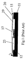
  • FIG. 1 depicts a cross sectional view of such a package.
  • the substrate 11 has a cavity 12 on the bottom side.
  • An integrated circuit die 17 is placed in the cavity upside down, so that the bottom of the integrated circuit die 17 is in physical contact with the substrate 11, and the bond pads of the die 17 are oriented pointing downwards towards the bottom of the finished package.
  • bond wires 19 are used to couple the input and output bonding pads of the integrated circuit 17 to conductive traces 20 of gold, aluminum, copper or other conductors which are formed on the bottom of the substrate 11.
  • the signal traces 20 lead to ball receptacle pads (not visible) on the substrate 11, to which the solder balls 15 are attached. Potting material 23 is then used to cover the die cavity and thus protect the integrated circuit 17 and the bond wires 19 and the signal traces from contamination, particulates, and moisture.
  • the cavity down package of FIG. 1 has some advantages over the prior art packages described above.
  • the use of throughhole connections is eliminated because the traces and the solder balls are physically placed on the bottom of the substrate.
  • the substrate is in thermal contact with the bottom of the die, so that if a good thermal conductor is used for the substrate, the package provides excellent thermal performance.
  • Heat sinks or fins may be installed on the top of the package for more enhanced thermal performance.
  • a problem in producing a cavity down integrated circuit package is that the spacing available for the bond wires and the potting material is limited.
  • the vertical distance (labeled “t” in FIG. 1 ) available underneath the package is limited by the diameter of the solder balls.
  • the wires are routed from the bond pads of the integrated circuit to the signal traces on the substrate in such a manner that the wire loop height is placed well within the vertical area "t” , the distance available when the solder balls are attached.
  • This bond wire height requires a looping profile where the top of the loop can not be very high above the substrate surface, causing the wire to be almost parallel with, or at least very close to, the substrate surface.
  • the bond wires have to travel over the rings to reach the substrate signal traces.
  • a method and apparatus for creating a slight clearance for bond wires which need to cross over conductive traces or other obstacles without physically or electrically contacting the obstacles.
  • an integrated circuit is provided in a package with the cavity down, using bond wires almost parallel to the package substrate surface and having at least one wide power ring for providing power or ground voltages to the integrated circuit.
  • a method and apparatus for subsequently forming a package for the completed integrated circuit is provided.
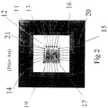
  • FIG. 2 depicts a bottom view of a prior art cavity down BGA integrated circuit package including a ground and power ring of the invention.
  • substrate 11 is shown with a die cavity 12 formed within it.
  • Ground and power rings 13 and 16 are formed of a conductor, typically a copper or copper alloy trace or a trace formed from another conventional conductor such as gold or gold alloys or other conductive alloys is formed on the surface of the substrate 11 and surrounding the die cavity 12.
  • the ground ring 13 is further coupled to a solder ball 15 which is designated as a ground pin for the completed integrated circuit. This coupling can be performed by a bond wire, or preferably by using a trace on the substrate, however it must cross a second power ring 16 without shorting rings 16 and 13 together.
  • Power ring 16 is provided surrounding ground ring 13, so that a supply and ground voltage ring may be used to power the integrated circuit.
  • Power ring 16 is coupled to a solder ball 14 which is designated as the power pin for the packaged integrated circuit using another trace formed on substrate 11.
  • Additional power and ground rings may be provided, for example, to lower resistance and eliminate noise by isolating switching circuitry power supplies from other power supplies as is known in the integrated circuit art.
  • some integrated circuits require multiple power supplies or ground supplies at different voltages, such as certain memory or DRAM devices.
  • the package disclosed herein uses at least one, and as many as necessary, power rings surrounding the die cavity.
  • Integrated circuit die 17 is placed within the die cavity 12 and mounted to the substrate using die attach epoxy, a thermally conductive tape, or other conventional integrated circuit die attach technology.
  • Bond pads 21 on the integrated circuit die 17 are coupled to the signal traces 20 on the substrate 11 by bond wires 19.
  • the bond wires 19 are comprised of gold, aluminum, silver, or other conductive alloys such as silver/gold, and are attached to the bond pads using conventional ball bonding techniques, that is the wire bonding station places a ball on the bond pad which is attached electrically and physically to the bond pads 21.
  • the bond wires 19 couple each bond pad to a signal trace 20 on the substrate.
  • the bond wires are attached to the signal traces using a stitch bond or other conventional bond for bond wires.
  • the bond wires 19 have to cross and remain electrically isolated from the ground ring 13 and power ring 16, except for bond wires which are intentionally bonded to either ring .
  • the integrated circuit die may have any one of a number of functions, including a memory device such as a DRAM, SRAM, EPROM, Synchronous DRAM, or other memory, a digital signal processor (DSP), a microprocessor, or a user specified function such as is found in ASICs, semicustom IC's, programmable gate arrays and other programmable or custom integrated circuits.
  • a memory device such as a DRAM, SRAM, EPROM, Synchronous DRAM, or other memory
  • DSP digital signal processor
  • microprocessor or a user specified function such as is found in ASICs, semicustom IC's, programmable gate arrays and other programmable or custom integrated circuits.
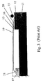
  • FIG. 3 depicts a cross sectional view of an embodiment, not preferred, which is illustrative of the results obtained in manufacturing the cavity down package of FIG. 2 using conventionally known wire bonding techniques.
  • substrate 11 is shown with a die cavity 12 formed within it.
  • Integrated circuit die 17 is placed within the cavity and attached using die attach epoxy or tape.
  • Bond pad 21 is shown with bond wire 19 attached to the bond pad using a ball type wire bond. Bond wire 19 is coupled across ground and power rings 13 and 16 to signal trace 20.
  • Solder ball 15 is attached to substrate 11 and electrically and physically coupled to signal trace 20.
  • FIG. 3 The arrangement of FIG. 3 is used to depict the problem addressed by the teachings disclosed herein.
  • the bond wire 19 is shown crossing the ground and power ring 13 and 16. It can be appreciated that the vertical clearance available between bond wire 19 and the ground and power rings 13 and 16 is not sufficient.
  • An integrated circuit package manufactured having this arrangement will exhibit undesired electrical shorts between bond wires 19 and one of the power rings due to the lack of proper clearance between the bond wires 19 and the power rings.
  • FIG. 4 is a close up view of a portion of the cross sectional view of FIG. 3 with the ball 15 omitted, though it can be part of the package and further illustrates the problem depicted in FIG. 3.
  • bond wire 19 crosses ground ring 13 and power ring 16 (in this example, although other examples, such as a single ground ring, are also contemplated) to couple the signal trace 20 formed on substrate 11 to the bond pad of integrated circuit 21. It can be appreciated that the bond wire 19 is too close to the ground and power rings 13 and 16 to provide adequate clearance to prevent unintentional connection and electrical shorting between bond wires 19 and the power rings. Also, even if actual contact is not made, cross talk may occur between the bond wires and the power rings, because the distance is so small between them.
  • FIG. 4 would exhibit similar problems.
  • the bond wires would also have to cross the power and ground rings and thus the possibility of a shorting problem would arise.
  • the invention described herein is applicable to BGA, PGA and other packaging arrangements where bond wires must cross power and ground signals, or other structures, without contacting them, that is, wherever a bond wire clearance problem arises.
  • FIG. 5 is a cross sectional view of a preferred embodiment of the package depicted as a bottom view in FIG. 2, using the method and apparatus of the invention.
  • substrate 11 is depicted in a partial cross section with die cavity 12 containing integrated circuit die 17.
  • Balls 15, as shown in FIG. 3 can be included though they are not shown Bond wire 19 couples bond pad 21 to signal trace 20.
  • Bond wire 19 has a ball type wire bond at die pad 21. Bond wire 19 is routed across power rings 13 and 16 and is then stitch bonded to ball bond 24, which has previously been placed on or near the innermost end of signal trace 20.
  • Ball bond 24 is made using a conventional ball bonding technique to make the ball, then skipping the normal looping and stitch bond sequences, going directly to wire break which would then occur above the ball, so that a ball is left on the inner end of signal trace 20. This operation is performed prior to the wire bonding of the bond pads 21 to the signal traces 20.
  • the wire bonding operation can be performed in any of several ways, including first forming the ball bonds 24 on each signal trace 20 of the substrate, then using a ball and stitch connection to couple each die pad 21 to the associated signal trace 20 by placing the ball wire bond on the die pad 21 and then forming a stitch wire bond on top of the ball bond 24.
  • a conventional wire bonder may be set up to form each connection in series, by first forming the ball bond on the particular signal trace 20, then moving to the associated bond pad 21 and forming a second ball bond, pulling the bond wire 19 to the signal trace 20 and placing a stitch bond on top of ball 24.
  • the advantage of this arrangement is that the clearance between the bond wires 19 that cross the power rings 13 and 16 is now increased by the height of the ball bond 24. This distance increase eliminates the potential for shorting between the bond wire 19 and the power rings 13 and 16.
  • FIG. 5 depicts two rings, 13 and 16, surrounding the die cavity. In a simpler example, perhaps only one ring would be used. Also, in the case of a bond pad that needs to be coupled to the power ring, 16, in the two ring example of FIG. 5, a spacer bond wire ball will be necessary between the bond wire and the power ring 16 to create the clearance needed to cross the ground ring 13. Additional rings could be used, in which case any bond wire that must cross any number of the rings would have the spacer bond ball of the invention placed between it and the ring or signal trace it couples to.
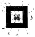
  • FIG. 6 there is shown a view as in FIG. 2 except that the balls 24 have been formed on the portion of the signal trace 20 close to the two rings 13 and 16 to provide elevation of the wires 19 in the vicinity of the two rings as shown in FIG. 5.
  • the balls 24 preferably have a height equal to the otherwise highest point on the underside of the substrate, though this height is not critical and can be greater or less than the otherwise highest point. It is clear that the higher the balls 24, the less likelihood there is for the wires 19 to sag toward the two rings 13 and 16. However, the height of the balls 24 can also affect the ultimate thickness of the package. Accordingly, there is generally a tradeoff between the height of the balls and consideration of ultimate package thickness.
  • the wires 19 are connected to the balls 24 preferably by a stitch bond.
  • the method and apparatus of the invention may be used to create a clearance tolerance wherever a bond wire must cross another structure without contacting it.
  • Examples include a PGA package with power and ground rings, or other bonded package types where the bond wires cross substrate traces or other materials that the bond wires should not contact.
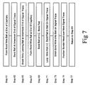
  • FIG. 7 depicts the bonding steps required to make the preferred embodiment of FIG. 5 in one preferred method.
  • wire bonders may perform the required operations in several different orders, each of which is contemplated within the scope of the invention and preferred embodiments disclosed within.
  • the method depicted in FIG. 6 illustrates one exemplary series of steps to be used in manufacturing the BGA package of the invention, but is not to be construed as limiting the scope of the invention to this particular order of steps.
  • a wire bonder bond head receives bond wire from a continuos supply of bond wire.
  • a conventional "flame off" technique is used for forming a ball bond at the end of the wire on the bonder head as is known in the wire bonding art.
  • the bonder head places the ball bond at the innermost end of a signal trace 20.
  • the bond wire is pulled from the ball as is known in the bonding art. This leaves the ball bond 24 on the end of signal trace 20.
  • Step 67 us a repeat of step 61, using a conventional "flame off” technique to make a ball at the end of the bond wire.
  • step 69 the bonder head approaches the associated bond pad 21 from above.
  • the end of the bond wire is again a ball shape.
  • this ball is placed on the bond pad.
  • Conventional techniques for bonding to the bond pad including the use of ultrasonic energy, vibration and pressure to improve the physical and electrical bond to the bond pad are used to achieve a reliable wire bond.
  • step 71 the bond head moves away from the bond pad 21, but this time the wire is not severed but remains coupled to bond pad 21. The bond wire 19 is then extended away from bond pad 21.
  • step 73 the bond head approaches previously formed and deposited ball bond 24 extending the bond wire 19 from bond pad 21.
  • the bond wire is stretched across the die cavity and across the power rings 13 and 16.
  • the wire bonder then forms a stitch type wire bond on the ball 24.
  • step 77 the wire bond is completed when a stitch wire bond is used to place the end of bond wire 19 on the ball bond 25 and the wire is severed. A flame off is used to form another ball for the next ball bond operation.
  • the bonder head is then positioned over the next signal trace on the substrate.
  • Step 77 shows the repeat operation step for the process.
  • the steps of FIG. 6 are then repeated for each bond pad and signal trace in the package.
  • a low looping wire bond wire is extended from each bond pad to a signal trace and routed across the power rings for each signal.
  • FIG. 7 The steps described in FIG. 7 are but one possible sequence which could be used to accomplish the apparatus of FIG. 5.
  • An alternative would be to form all of the bond wire balls on the innermost ends of the signal traces of substrate 11, and then to bond the IC bond pads to the associated bond wire balls in sequence.
  • Vdd additional supply voltages
  • These rings will also surround the cavity and can be made inside or outside the ground ring. These will also be coupled by bond wires to more than one bond pad on a typical IC. If these rings lie outside a first ground ring, then a clearance issue will exist and a bond wire ball should be provided prior to bonding the power ring to the bond pads of the IC, so that the wire can cross the inner ring without a shorting or clearance problem.
  • the method disclosed above in FIG. 7 is preferably used to perform this step.

Landscapes

  • Engineering & Computer Science (AREA)
  • Computer Hardware Design (AREA)
  • Microelectronics & Electronic Packaging (AREA)
  • Power Engineering (AREA)
  • Physics & Mathematics (AREA)
  • Condensed Matter Physics & Semiconductors (AREA)
  • General Physics & Mathematics (AREA)
  • Wire Bonding (AREA)
EP19980116369 1997-09-19 1998-08-28 Verfahren und Vorrichtung für drahtgebondete Verpackung für integrierte Schaltung Withdrawn EP0903780A3 (de)

Applications Claiming Priority (2)

Application Number Priority Date Filing Date Title
US5953997P 1997-09-19 1997-09-19
US59539P 1997-09-19

Publications (2)

Publication Number Publication Date
EP0903780A2 true EP0903780A2 (de) 1999-03-24
EP0903780A3 EP0903780A3 (de) 1999-08-25

Family

ID=22023622

Family Applications (1)

Application Number Title Priority Date Filing Date
EP19980116369 Withdrawn EP0903780A3 (de) 1997-09-19 1998-08-28 Verfahren und Vorrichtung für drahtgebondete Verpackung für integrierte Schaltung

Country Status (6)

Country Link
US (1) US6194786B1 (de)
EP (1) EP0903780A3 (de)
JP (1) JPH11251355A (de)
KR (1) KR19990029932A (de)
SG (1) SG68074A1 (de)
TW (1) TW436949B (de)

Cited By (2)

* Cited by examiner, † Cited by third party
Publication number Priority date Publication date Assignee Title
US6753594B2 (en) 2001-08-22 2004-06-22 Infineon Technologies Ag Electronic component with a semiconductor chip and fabrication method
WO2004053986A1 (en) * 2002-12-10 2004-06-24 Koninklijke Philips Electronics N.V. High density package interconnect power and ground strap and method therefor

Families Citing this family (38)

* Cited by examiner, † Cited by third party
Publication number Priority date Publication date Assignee Title
US6933594B2 (en) * 1998-06-10 2005-08-23 Asat Ltd. Leadless plastic chip carrier with etch back pad singulation
US8330270B1 (en) 1998-06-10 2012-12-11 Utac Hong Kong Limited Integrated circuit package having a plurality of spaced apart pad portions
US6229200B1 (en) 1998-06-10 2001-05-08 Asat Limited Saw-singulated leadless plastic chip carrier
US6872661B1 (en) 1998-06-10 2005-03-29 Asat Ltd. Leadless plastic chip carrier with etch back pad singulation and die attach pad array
US7271032B1 (en) 1998-06-10 2007-09-18 Asat Ltd. Leadless plastic chip carrier with etch back pad singulation
US7226811B1 (en) 1998-06-10 2007-06-05 Asat Ltd. Process for fabricating a leadless plastic chip carrier
US7247526B1 (en) 1998-06-10 2007-07-24 Asat Ltd. Process for fabricating an integrated circuit package
US6635957B2 (en) * 1998-06-10 2003-10-21 Asat Ltd. Leadless plastic chip carrier with etch back pad singulation and die attach pad array
US6989294B1 (en) 1998-06-10 2006-01-24 Asat, Ltd. Leadless plastic chip carrier with etch back pad singulation
US7270867B1 (en) 1998-06-10 2007-09-18 Asat Ltd. Leadless plastic chip carrier
JP2000260809A (ja) * 1999-03-12 2000-09-22 Toshiba Corp 半導体装置のパッケージ
US6735651B1 (en) * 1999-07-30 2004-05-11 International Business Machines Corporation Multi-chip module having chips coupled in a ring
US6518663B1 (en) * 1999-08-30 2003-02-11 Texas Instruments Incorporated Constant impedance routing for high performance integrated circuit packaging
JP2001168223A (ja) * 1999-12-07 2001-06-22 Fujitsu Ltd 半導体装置
US6621280B1 (en) * 2000-06-27 2003-09-16 Agere Systems Inc. Method of testing an integrated circuit
US6525553B1 (en) * 2000-09-11 2003-02-25 St Assembly Test Services Ltd. Ground pin concept for singulated ball grid array
US6770963B1 (en) * 2001-01-04 2004-08-03 Broadcom Corporation Multi-power ring chip scale package for system level integration
WO2003036490A1 (en) * 2001-10-24 2003-05-01 Bea Systems, Inc. System and method for xml data representation of portlets
US6674176B2 (en) * 2002-02-20 2004-01-06 Lsi Logic Corporation Wire bond package with core ring formed over I/O cells
US6777803B2 (en) * 2002-08-28 2004-08-17 Lsi Logic Corporation Solder mask on bonding ring
US7732914B1 (en) 2002-09-03 2010-06-08 Mclellan Neil Cavity-type integrated circuit package
US6815836B2 (en) * 2003-03-24 2004-11-09 Texas Instruments Incorporated Wire bonding for thin semiconductor package
TWI242275B (en) * 2003-05-16 2005-10-21 Via Tech Inc Multi-column wire bonding structure and layout method for high-frequency IC
CN100336218C (zh) * 2003-08-25 2007-09-05 威盛电子股份有限公司 一种高频集成电路多排线打线结构及方法
CN1332445C (zh) * 2003-10-09 2007-08-15 威盛电子股份有限公司 一种高频集成电路多排线打线结构
US7009286B1 (en) 2004-01-15 2006-03-07 Asat Ltd. Thin leadless plastic chip carrier
US7411289B1 (en) 2004-06-14 2008-08-12 Asat Ltd. Integrated circuit package with partially exposed contact pads and process for fabricating the same
US7091581B1 (en) 2004-06-14 2006-08-15 Asat Limited Integrated circuit package and process for fabricating the same
US7595225B1 (en) 2004-10-05 2009-09-29 Chun Ho Fan Leadless plastic chip carrier with contact standoff
JP4964780B2 (ja) * 2004-11-12 2012-07-04 スタッツ・チップパック・インコーポレイテッド ワイヤボンド相互接続、半導体パッケージ、および、ワイヤボンド相互接続の形成方法
US7868468B2 (en) * 2004-11-12 2011-01-11 Stats Chippac Ltd. Wire bonding structure and method that eliminates special wire bondable finish and reduces bonding pitch on substrates
US7358119B2 (en) * 2005-01-12 2008-04-15 Asat Ltd. Thin array plastic package without die attach pad and process for fabricating the same
JP4558539B2 (ja) * 2005-03-09 2010-10-06 日立協和エンジニアリング株式会社 電子回路用基板、電子回路、電子回路用基板の製造方法および電子回路の製造方法
US7348663B1 (en) 2005-07-15 2008-03-25 Asat Ltd. Integrated circuit package and method for fabricating same
US7410830B1 (en) 2005-09-26 2008-08-12 Asat Ltd Leadless plastic chip carrier and method of fabricating same
US7701049B2 (en) * 2007-08-03 2010-04-20 Stats Chippac Ltd. Integrated circuit packaging system for fine pitch substrates
US7911040B2 (en) * 2007-12-27 2011-03-22 Stats Chippac Ltd. Integrated circuit package with improved connections
US8106474B2 (en) * 2008-04-18 2012-01-31 Semiconductor Energy Laboratory Co., Ltd. Semiconductor device

Family Cites Families (26)

* Cited by examiner, † Cited by third party
Publication number Priority date Publication date Assignee Title
GB1224562A (en) * 1967-05-16 1971-03-10 Texas Instruments Inc An etching process
FR2573272A1 (fr) * 1984-11-14 1986-05-16 Int Standard Electric Corp Procede de realisation d'un substrat comportant un conducteur coaxial
EP0262530B1 (de) * 1986-09-23 1993-06-23 Siemens Aktiengesellschaft Halbleiterbauelemente mit Leistungs-MOSFET und Steuerschaltung
GB2201545B (en) * 1987-01-30 1991-09-11 Tanaka Electronics Ind Method for connecting semiconductor material
JPH0249447A (ja) * 1988-05-20 1990-02-19 Hitachi Ltd 半導体装置とその製造方法
JP2592308B2 (ja) * 1988-09-30 1997-03-19 株式会社日立製作所 半導体パッケージ及びそれを用いたコンピュータ
JPH02184054A (ja) * 1989-01-11 1990-07-18 Toshiba Corp ハイブリッド型樹脂封止半導体装置
US5045151A (en) * 1989-10-17 1991-09-03 Massachusetts Institute Of Technology Micromachined bonding surfaces and method of forming the same
US5296744A (en) * 1991-07-12 1994-03-22 Vlsi Technology, Inc. Lead frame assembly and method for wiring same
JP2801810B2 (ja) * 1992-04-14 1998-09-21 株式会社東芝 樹脂封止型半導体装置
US5366589A (en) * 1993-11-16 1994-11-22 Motorola, Inc. Bonding pad with circular exposed area and method thereof
US5578869A (en) * 1994-03-29 1996-11-26 Olin Corporation Components for housing an integrated circuit device
US5530287A (en) * 1994-09-14 1996-06-25 Unisys Corporation High density wire bond pattern for integratd circuit package
US5808872A (en) * 1994-11-15 1998-09-15 Nippon Steel Corporation Semiconductor package and method of mounting the same on circuit board
US5808354A (en) * 1994-11-21 1998-09-15 Samsung Electronics Co., Ltd. Lead frame for a semiconductor device comprising inner leads having a locking means for preventing the movement of molding compound against the inner lead surface
US5622588A (en) * 1995-02-02 1997-04-22 Hestia Technologies, Inc. Methods of making multi-tier laminate substrates for electronic device packaging
JPH08330346A (ja) * 1995-05-31 1996-12-13 Nec Kyushu Ltd 半導体装置の製造方法
US5736792A (en) * 1995-08-30 1998-04-07 Texas Instruments Incorporated Method of protecting bond wires during molding and handling
TW353223B (en) * 1995-10-10 1999-02-21 Acc Microelectronics Corp Semiconductor board providing high signal pin utilization
KR0156334B1 (ko) * 1995-10-14 1998-10-15 김광호 차폐 본딩 와이어를 구비하는 고주파, 고밀도용 반도체 칩 패키지
JPH09199549A (ja) * 1996-01-22 1997-07-31 Denso Corp ワイヤボンディング方法
US6001724A (en) * 1996-01-29 1999-12-14 Micron Technology, Inc. Method for forming bumps on a semiconductor die using applied voltage pulses to an aluminum wire
US5764486A (en) * 1996-10-10 1998-06-09 Hewlett Packard Company Cost effective structure and method for interconnecting a flip chip with a substrate
US6098283A (en) * 1996-12-19 2000-08-08 Intel Corporation Method for filling vias in organic, multi-layer packages
US5976964A (en) * 1997-04-22 1999-11-02 Micron Technology, Inc. Method of improving interconnect of semiconductor device by utilizing a flattened ball bond
US5973397A (en) * 1997-10-22 1999-10-26 Lsi Logic Corporation Semiconductor device and fabrication method which advantageously combine wire bonding and tab techniques to increase integrated circuit I/O pad density

Cited By (2)

* Cited by examiner, † Cited by third party
Publication number Priority date Publication date Assignee Title
US6753594B2 (en) 2001-08-22 2004-06-22 Infineon Technologies Ag Electronic component with a semiconductor chip and fabrication method
WO2004053986A1 (en) * 2002-12-10 2004-06-24 Koninklijke Philips Electronics N.V. High density package interconnect power and ground strap and method therefor

Also Published As

Publication number Publication date
TW436949B (en) 2001-05-28
US6194786B1 (en) 2001-02-27
EP0903780A3 (de) 1999-08-25
KR19990029932A (ko) 1999-04-26
JPH11251355A (ja) 1999-09-17
SG68074A1 (en) 1999-10-19

Similar Documents

Publication Publication Date Title
US6194786B1 (en) Integrated circuit package providing bond wire clearance over intervening conductive regions
US7012323B2 (en) Microelectronic assemblies incorporating inductors
US5376588A (en) Method for making high pin count package for semiconductor device
US5352632A (en) Multichip packaged semiconductor device and method for manufacturing the same
US6724071B2 (en) Molded plastic package with heat sink and enhanced electrical performance
US7217997B2 (en) Ground arch for wirebond ball grid arrays
US5332864A (en) Integrated circuit package having an interposer
JP2819285B2 (ja) 積層型ボトムリード半導体パッケージ
US8637975B1 (en) Semiconductor device having lead wires connecting bonding pads formed on opposite sides of a core region forming a shield area
US20010017411A1 (en) Semiconductor chip and semiconductor device having the chip
JPH1092972A (ja) 集積回路用パッケージ
US20040124545A1 (en) High density integrated circuits and the method of packaging the same
GB2329068A (en) A vertical interconnect package for electronic components
US6790760B1 (en) Method of manufacturing an integrated circuit package
US6465882B1 (en) Integrated circuit package having partially exposed conductive layer
US7173341B2 (en) High performance thermally enhanced package and method of fabricating the same
US5704593A (en) Film carrier tape for semiconductor package and semiconductor device employing the same
US20060125079A1 (en) High density package interconnect wire bond strip line and method therefor
US5982026A (en) Inexpensive resin molded semiconductor device
JP2803656B2 (ja) 半導体装置
US20050253245A1 (en) Package design and method for electrically connecting die to package
JP3234614B2 (ja) 半導体装置及びその製造方法
KR20010059916A (ko) 멀티칩 모듈 반도체패키지
JP3210503B2 (ja) マルチチップモジュールおよびその製造方法
JP2990120B2 (ja) 半導体装置

Legal Events

Date Code Title Description
PUAI Public reference made under article 153(3) epc to a published international application that has entered the european phase

Free format text: ORIGINAL CODE: 0009012

AK Designated contracting states

Kind code of ref document: A2

Designated state(s): DE FR GB IT NL

AX Request for extension of the european patent

Free format text: AL;LT;LV;MK;RO;SI

PUAL Search report despatched

Free format text: ORIGINAL CODE: 0009013

AK Designated contracting states

Kind code of ref document: A3

Designated state(s): AT BE CH CY DE DK ES FI FR GB GR IE IT LI LU MC NL PT SE

AX Request for extension of the european patent

Free format text: AL;LT;LV;MK;RO;SI

RIC1 Information provided on ipc code assigned before grant

Free format text: 6H 01L 21/60 A, 6H 01L 23/49 B, 6H 01L 21/48 B, 6B 23K 20/00 B

17P Request for examination filed

Effective date: 20000223

AKX Designation fees paid

Free format text: DE FR GB IT NL

STAA Information on the status of an ep patent application or granted ep patent

Free format text: STATUS: THE APPLICATION IS DEEMED TO BE WITHDRAWN

18D Application deemed to be withdrawn

Effective date: 20060908