EP0902424A1 - Méthode et appareil d'enregistrement d'information pour la réduction du sautillement dans les flancs des marques - Google Patents
Méthode et appareil d'enregistrement d'information pour la réduction du sautillement dans les flancs des marques Download PDFInfo
- Publication number
- EP0902424A1 EP0902424A1 EP98116819A EP98116819A EP0902424A1 EP 0902424 A1 EP0902424 A1 EP 0902424A1 EP 98116819 A EP98116819 A EP 98116819A EP 98116819 A EP98116819 A EP 98116819A EP 0902424 A1 EP0902424 A1 EP 0902424A1
- Authority
- EP
- European Patent Office
- Prior art keywords
- power level
- pulse
- energy beam
- information
- mark portion
- Prior art date
- Legal status (The legal status is an assumption and is not a legal conclusion. Google has not performed a legal analysis and makes no representation as to the accuracy of the status listed.)
- Granted
Links
Images


Classifications
-
- G—PHYSICS
- G11—INFORMATION STORAGE
- G11B—INFORMATION STORAGE BASED ON RELATIVE MOVEMENT BETWEEN RECORD CARRIER AND TRANSDUCER
- G11B7/00—Recording or reproducing by optical means, e.g. recording using a thermal beam of optical radiation by modifying optical properties or the physical structure, reproducing using an optical beam at lower power by sensing optical properties; Record carriers therefor
- G11B7/004—Recording, reproducing or erasing methods; Read, write or erase circuits therefor
- G11B7/006—Overwriting
- G11B7/0062—Overwriting strategies, e.g. recording pulse sequences with erasing level used for phase-change media
-
- G—PHYSICS
- G11—INFORMATION STORAGE
- G11B—INFORMATION STORAGE BASED ON RELATIVE MOVEMENT BETWEEN RECORD CARRIER AND TRANSDUCER
- G11B7/00—Recording or reproducing by optical means, e.g. recording using a thermal beam of optical radiation by modifying optical properties or the physical structure, reproducing using an optical beam at lower power by sensing optical properties; Record carriers therefor
- G11B7/004—Recording, reproducing or erasing methods; Read, write or erase circuits therefor
- G11B7/0045—Recording
- G11B7/00454—Recording involving phase-change effects
-
- G—PHYSICS
- G11—INFORMATION STORAGE
- G11B—INFORMATION STORAGE BASED ON RELATIVE MOVEMENT BETWEEN RECORD CARRIER AND TRANSDUCER
- G11B7/00—Recording or reproducing by optical means, e.g. recording using a thermal beam of optical radiation by modifying optical properties or the physical structure, reproducing using an optical beam at lower power by sensing optical properties; Record carriers therefor
- G11B7/004—Recording, reproducing or erasing methods; Read, write or erase circuits therefor
- G11B7/006—Overwriting
-
- G—PHYSICS
- G11—INFORMATION STORAGE
- G11B—INFORMATION STORAGE BASED ON RELATIVE MOVEMENT BETWEEN RECORD CARRIER AND TRANSDUCER
- G11B7/00—Recording or reproducing by optical means, e.g. recording using a thermal beam of optical radiation by modifying optical properties or the physical structure, reproducing using an optical beam at lower power by sensing optical properties; Record carriers therefor
- G11B7/12—Heads, e.g. forming of the optical beam spot or modulation of the optical beam
- G11B7/125—Optical beam sources therefor, e.g. laser control circuitry specially adapted for optical storage devices; Modulators, e.g. means for controlling the size or intensity of optical spots or optical traces
- G11B7/126—Circuits, methods or arrangements for laser control or stabilisation
-
- G—PHYSICS
- G11—INFORMATION STORAGE
- G11B—INFORMATION STORAGE BASED ON RELATIVE MOVEMENT BETWEEN RECORD CARRIER AND TRANSDUCER
- G11B20/00—Signal processing not specific to the method of recording or reproducing; Circuits therefor
- G11B20/10—Digital recording or reproducing
- G11B20/10009—Improvement or modification of read or write signals
-
- G—PHYSICS
- G11—INFORMATION STORAGE
- G11B—INFORMATION STORAGE BASED ON RELATIVE MOVEMENT BETWEEN RECORD CARRIER AND TRANSDUCER
- G11B20/00—Signal processing not specific to the method of recording or reproducing; Circuits therefor
- G11B20/10—Digital recording or reproducing
- G11B20/14—Digital recording or reproducing using self-clocking codes
- G11B20/1403—Digital recording or reproducing using self-clocking codes characterised by the use of two levels
- G11B20/1423—Code representation depending on subsequent bits, e.g. delay modulation, double density code, Miller code
- G11B20/1426—Code representation depending on subsequent bits, e.g. delay modulation, double density code, Miller code conversion to or from block codes or representations thereof
-
- G—PHYSICS
- G11—INFORMATION STORAGE
- G11B—INFORMATION STORAGE BASED ON RELATIVE MOVEMENT BETWEEN RECORD CARRIER AND TRANSDUCER
- G11B7/00—Recording or reproducing by optical means, e.g. recording using a thermal beam of optical radiation by modifying optical properties or the physical structure, reproducing using an optical beam at lower power by sensing optical properties; Record carriers therefor
- G11B7/004—Recording, reproducing or erasing methods; Read, write or erase circuits therefor
- G11B7/0055—Erasing
- G11B7/00557—Erasing involving phase-change media
Definitions
- the present invention relates to a method and apparatus for recording information in an information recording medium by radiation of an energy beam, or more in particular to an information recording method very effective for a phase change optical disk and an information recording apparatus using such an information recording method.
- a conventional method of recording and erasing information in a rewritable record film is disclosed, for example, in JP-A-62-175948 (laid open August 1, 1987), which uses a magneto-optical disk of an exchange couple double-layered film as a record film.
- Another conventional method for recording and erasing information in a rewritable record film is disclosed in JP-A-62-259229 (laid open November 11, 1987), which uses a record film for a phase change optical disk capable of high-speed erasure by crystallization within substantially the same time as the laser radiation time for recording. In these cases, the power of an energy beam is alternated between at least two levels both higher than the read level, i.e.
- a record mark can be prevented from assuming a shape such that the rear portion of the record mark is wider than the front portion thereof by changing the energy beam between three levels including a high power level, an intermediate level and a power level lower than the intermediate level.
- the distance between centers of laser beams radiated onto a recording medium to form adjacent two mark portions thereon is small as compared with the diameter of the laser beam spot, with the result that light is considerably overlapped in distribution. It is necessary to prevent a record mark distortion caused by this phenomenon. In the case where the space portion between mark portions is short, the record mark edge position of a reproduced signal waveform shifts due to the fact that such mark portions cannot be resolved by the beam spot. This inconvenience is also required to be prevented.
- the object of the present invention is to provide an information recording method and apparatus capable of recording information with high density.
- the invention is suitable for recording information accurately in the case where the recording density is high and/or the relative speed between an energy beam and an information recording medium is high.
- a technique for reducing the track pitches is under development with the intention of increasing the recording density.
- a method exists, for example, in which information is recorded in both grooves and lands (areas between grooves) formed on an information recording medium. According to this method, crosstalks of reproduced signals from lands to grooves or from grooves to lands can be cancelled by setting the grooves to a proper depth (optical phase difference between lands and grooves).
- the heat generated by the energy beam is used for recording information. Therefore, thermal interferences occur to adjacent tracks (grooves adjacent to lands or lands adjacent to grooves) in the case where the energy beam position cannot be controlled in stable fashion. This leads to the problem that the information recorded in adjacent tracks is erased.
- the present invention is suitable for recording information accurately without erasing the information in adjacent tracks even in the case where the information is recorded in an information recording medium having narrow track pitches or especially an information recording medium corresponding to the land/groove recording scheme and in the case where the track pitches are not more than the diameter of the recording energy beam.
- Another crucial problem is how to improve the recording sensitivity.
- the energy beam passes a record mark on the information recording medium within a shorter time.
- the amount of energy radiated on the information recording medium in a unit time is reduced, and therefore the portion of the record film to be formed with a record mark is often insufficiently heated.
- accurate recording which can be accomplished with pulses of very narrow width, requires a high peak laser power.
- the present invention is also suitable for recording information accurately without a large energy beam power in the case where the relative speed between the information recording medium and the recording energy beam is increased and/or in the case where information is recorded in an information recording medium liable to be cooled rapidly.
- a method of recording information in a recording medium capable of being set in a first state of a second power level and in a second state of a third power level higher than the second power level of an energy beam, in which the energy beam is radiated while moving the energy beam and the recording medium relatively to each other and information in terms of the length and interval of mark portions in the second state is recorded in the recording medium
- the method comprising the first step of irradiating the recording medium with an energy beam of a first power level lower than the second and third power levels before and/or after recording the information, the second step of irradiating the recording medium with at least one pulse of one or more energy beam pulses of the third power level for forming a mark portion in the second state, and the third step of irradiating the recording medium, before or after the first pulse of one or more energy beam pulses for forming the mark portion, with an energy beam pulse of a radiation energy larger in the case where the mark portion in the second state has a first length than in the
- the third step can be replaced by an equivalent third step of, in the case where the space portion following a mark portion in the second state has a first length, irradiating the recording medium, after the last pulse of one or more energy beam pulses for forming the mark portion, with an energy beam pulse having an energy smaller than in the case where the space portion has a second length and at a power level lower than the second power level.
- a method of recording information in the form of space and mark portions on a recording medium capable of assuming first and second physical states corresponding to space and mark portions of information, respectively, the recording medium being irradiated, to produce a length of a portion of the recording medium in the second physical state, with an energy beam being movable relative to the recording medium and being modulated to have power levels varying with time in a pulse waveform in accordance with a mark portion of information, wherein:
- an apparatus for recording information in a recording medium capable being set in a first state of a second power level and in a second state of a third power level higher than the second power level of an energy beam
- the apparatus comprising an energy beam radiation means and means for moving the energy beam and the recording medium relative to each other, the information being recorded on the recording medium in the form of length and space of a mark portion in the second state
- the energy beam radiation means includes a waveform generating circuit having first means for irradiating the recording medium with a beam of a first power level (P1) lower than the second and third power levels before and/or after recording the information, second means for irradiating the recording medium with at least a pulse of one or more energy beam pulses of the third power level for forming a mark portion in the second state, and third means for increasing the radiation energy in the case where the mark portion in the second state has a first length as compared with when said mark portion in said second state has a second length, before or after the first
- an apparatus for recording information in a recording medium capable of being set in a first state of a second power level and in a second state of a third power level higher than the second power level of an energy beam, comprising energy beam radiation means and means for moving the energy beam and the recording medium relative to each other, the information being recorded on the recording medium in the form of length and interval of a mark portion in the second state
- the energy beam radiation means includes a waveform generating circuit having first means for irradiating the recording medium with a beam of a first power level (P1) lower than the second and third power levels before and/or after recording the information, second means for irradiating the recording medium with at least a pulse of one or more energy beam pulses of the third power level for forming a mark portion in the second state, and third means for irradiating the recording medium, in the case where the space portion after a mark portion in the second state has a first length, with an energy smaller than when the space portion following the mark portion has
- At least an energy beam pulse train for forming a mark portion is defined as a train of pulses for forming a mark portion arranged substantially equidistantly with a shorter interval than the channel clock in the recording apparatus.
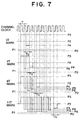
- Fig. 1 shows a sectional structure of a disk-shaped information recording medium according to an embodiment. This medium can be fabricated in the following manner.
- a polycarbonate base 12 cm in diameter and 0.6 mm in thickness having tracking guide grooves for land/groove recording at pitches of 0.6 ⁇ m in the surface thereof is formed with an Al 2 O 3 heat diffusion layer 12 about 30 nm thick.
- An 80ZnS-20SiO 2 protective layer 13 about 45 nm thick is formed.
- a SiO 2 protective layer 14 about 5 nm thick is formed.
- a Ge 14 Sb 28 Te 58 record film 15 about 15 nm thick and a SiO 2 intermediate layer 16 about 5 nm thick are formed.
- an absorption difference adjusting layer 17 about 18 nm thick made of an 80Mo-20SiO 2 film is formed, followed by a first reflective layer 18 of 89Al-11Ti about 70 nm thick and a second reflective layer 19 of 97Al-3Ti film about 70 nm thick, in that order.
- a layered film can be formed by a magnetron sputtering device.
- a protective film 20 is formed on the resulting assembly using an ultraviolet radiation curable resin. In this way, a first disk member is prepared.
- a second disk member having the same configuration as the first disk member is prepared.
- the first disk member and the second disk member are attached to each other by the ends thereof nearer to the second reflective film through an adhesive layer, thereby fabricating a disk-shaped information recording medium.
- the record film 15 of the first disk member constituting the recording medium fabricated in the above-mentioned way is initialized in the manner described as follows. This is exactly the case with the record film of the second disk member. The description that follows, therefore, will be made only about the record film 15 of the first disk member.
- the medium is rotated at a constant linear velocity of 8 m/s, and laser beam power of 900 mW of a semiconductor laser (wavelength of about 810 nm) having an elliptical spot along the radius of the medium is radiated on the record film 15 through the polycarbonate base 11.
- the recording head is driven while automatically focusing the laser beam on the record film 15.
- the laser beam spot is displaced by one sixteenth of the spot length each time along the radius of the medium. In this way, the medium is crystallized (the first physical state).
- the tracking and the automatic focusing are effected with a laser beam of a first power level P1 (1 mW) constituting a read power level while radiating the disk.
- P1 1 mW
- the laser beam power is raised to a second power level for erasing the unrequired written information by crystallization.
- the power is further raised to a third level.
- the mark portion The record waveform for forming this record mark (hereinafter referred to as "the mark portion") will be described in detail later.
- the power ratio between the third power level and the second power level is preferably 1:0.3 to 1:0.8.
- new information can be recorded by overwriting it directly on the old information recorded in the particular portion.
- an overwrite operation with a single circular light spot is possible.
- the motor is controlled by a ZCLV (Zone Constant Linear Velocity) method in which the rotational speed of the disk is varied from one zone to another for recording or reproduction. In this format, therefore, the disk linear velocity is different between the innermost circumference and outermost circumference in each zone.
- ZCLV Zero Constant Linear Velocity
- Information (digital signal) inputted from outside the recording apparatus is transmitted to an 8-16 modulator in units of 8 bits.
- 8 bits of information is converted to 16 bits of information by use of a recording method called the 8-16 modulation scheme.
- information of 3T to 11T in mark length corresponding to 8-bit information is recorded on the disk (medium) 1 rotationally driven by the motor 2.
- the 8-16 modulator 8 performs the modulation for this purpose.
- T designates a clock period for information recording and is 15.6 ns in the case under consideration.
- a preferable value of T in the method according to this embodiment is in the range between 5 ns and 20 ns inclusive.
- the digital signal of 3T to 11T converted by the 8-16 modulator 8 is transferred to a record waveform generating circuit 6 thereby to generate a record waveform.
- the basic width of each pulse constituting a pulse train of the third power level for forming a mark portion is assumed to be T or T/2, and the width of the pulse lower than the second power level following the pulse train, i.e. the cooling pulse width Tc can be changed from outside.
- the record waveform containing the pulse train generated by the record waveform generating circuit 6 is transferred to a laser driving circuit 7, which emits a semiconductor laser in an optical head 3 based on the same record waveform.
- the laser beam is circularly polarized.
- This recording apparatus corresponds to what is called the land/groove recording scheme in which information is recorded in both grooves and lands (areas between grooves). In this recording apparatus, either the lands or the grooves can be arbitrarily selected for tracking by a land/groove servo circuit.
- the recorded information can also be reproduced by use of the optical head.
- a laser beam focused to the same size as at the time of recording is radiated on the disk, and the light reflected from the mark portion and the portion (space portion) other than the mark portion is detected thereby to obtain a reproduced signal.
- the amplitude of this reproduced signal is amplified by a pre-amplifier 4 and transferred to an 8-16 demodulator 10.
- the 8-16 demodulator 10 converts each 16 bits into 8-bit information. The foregoing operation completes the reproduction of the mark portion recorded.
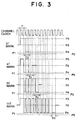
- Fig. 3 shows a well-known record waveform as a reference.
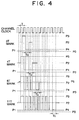
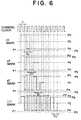
- Figs. 4 to 9 are diagrams for explaining record waveforms according to an embodiment of the invention.
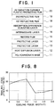
- P3 designates the power of the third power level capable of forming a mark portion
- P2 the power of the second power level for achieving the crystallization of the record film of the medium
- P1 the power of the first power level for read operation.
- T designates the width of a channel clock.
- the basic width of the laser beam pulse radiated on the medium is T/2, and the pulse interval is also T/2.
- Fig. 3 shows only the laser beam pulse waveforms for forming mark portions of 3T, 4T, 6T and 11T.
- the mark portions of 5T to 10T are formed by adding a set of waveforms including T/2 high power level and T/2 low power level, respectively, following the first pulse of the waveform of 4T.
- the mark portion of 11T is the result of addition of seven sets.
- a pulse train longer than 11T can be obtained by adding waveforms in similar fashion.
- the width of the first pulse of the laser beam pulse train is given as 1T, the width of the last pulse also as 1T, and the width of other pulses as T/2.
- the record film is preferably cooled by lowering the laser power to a level lower than the second power level. This pulse of low power level is called the cooling pulse.
- the power level reached by this pulse is assumed to be a fourth power level. Also assume that
- An object of the present invention is to predict and record these phenomena and thereby to make possible an ultrahigh density recording with the length of the shortest mark (space) portion not more than one half the diameter of the laser beam spot.
- the power is at the second level P2 of 5 mW, for example, before a mark portion is formed.
- the power rises toward and reaches the third power level P3 of 10.5 mW, for example.
- the radiation of the laser beam of the third power level melts the record film, which is then rapidly cooled into an amorphous state (second physical state).
- the laser of the 1T-wide third power level is radiated for recording.
- the energy beam pulse waveform has a mark edge adjusting pulse before the pulse train (information pulses) for forming a mark portion.
- the energy beam is raised to a fifth power level P5 0.1 mW higher than the second power level P2 before being raised to the third power level P3.
- the energy beam is raised to the third power level P3.
- the rise of energy level (i.e. preheating) from the power level P2 to power level P5 is effective as in the following case if in the range of 0.05 mW to 2.0 mW (i.e.
- third power level (P3) less second power level (P2) is 5.5 mW.
- the time after reaching the fifth power level P5 before being raised to the third power level is preferably 0.1T to 1.5T for the 5T mark portion, 0.1T to 2.0T for the 6T mark portion, and 0.1T to 1.5T for the 7T mark portion.
- the fifth power level P5 can be changed according to the mark portion length within the range of power level described above, in such manner that P5 (6T) > P5 (5T) > P5 (7T). In this way, the leading edge jitter can be suppressed in similar fashion.
- the mark portion length subjected to preheating is not limited to 5T, 6T, 7T but can include 3T, 4T or 8T.
- the power is lowered from second power level P2 to sixth power level P6 with a mark edge adjusting pulse inserted following the first pulse in the energy beam pulse train (information pulse train) high in power level for forming a mark portion, and after the second pulse in the same pulse train, the fourth power level P4 is reached as a mark length adjusting pulse.
- the fourth power level is 1 mW
- the sixth power level P6 is raised from the fourth power level P4 by an amount between 0.05 mW and 5.0 mW inclusive. In this way, a similar effect of suppressing the leading edge is obtained.
- a preferred example of power difference between the sixth power level P6 and the fourth power level P4 is 0.05 mW to 3 mW for 5T mark, 0.10 mW to 5.0 mW for 6T mark, and 0.05 mW to 3.0 mW for 7T mark.
- the high power level that the first pulse in the energy beam pulse train (information pulse section) reaches for forming a mark portion is the third power level P3.
- the power level of the second pulse to the last pulse but one in the pulse train is the seventh power level P7
- the power level of the last pulse is the ninth power level P9.
- the third, seventh and ninth power levels can be the same.
- the seventh power level P7 is higher than the third power level P3 by 0.1 mW to 2.0 mW for the level P3 being 10.5 mW, however, the leading edge of the mark portion is advantageously prevented from growing excessively. Thus, the leading edge jitter can be suppressed to 12.5%.
- the leading edge jitter is advantageously lowered. As a result, the leading edge jitter is suppressed to 12%.
- the power level reached by lowering from the high power level P3 for forming a mark portion is the tenth power level P10 different from other pulses immediately before the last pulse and this power level P10 is raised to a level 0.1 mW to 2.0 mW higher than the level between the second pulse and the last pulse but one, i.e. the eighth power level. Then, the leading and trailing edge jitters can be reduced. Consequently, the average jitter at the leading and trailing edges can be suppressed to 7.5%.
- At least one of the fourth, sixth, eighth and tenth power levels P4, P6, P8 and P10, especially, the eighth power level P8, if lower than the first power level P1 providing a read power level, can be preferably realized simply by turning off the high frequency superposition of the semiconductor laser as the same amplifier output voltage as the first power level P1.
- Trailing edge jitters are determined with the width Tc of the cooling pulse being changed at intervals of T/2 during a period from 0T to 2.5T, the cooling pulse constituting a mark edge adjusting pulse section of the energy pulse waveform.
- Fig. 8 shows the dependency of the trailing edge jitter on the cooling pulse width. In the case where Tc is 0T, the jitter value is 18%, which changes to 8% when Tc is 1.5T. In this way, a superior reproduced signal can be obtained by optimizing the cooling pulse width Tc.
- the cooling pulse width Tc in the energy beam pulse train (pulse waveform) for recording a mark portion may be made larger when recording information with the second shortest space portion of 4T than when recording information with a space portion of other lengths. Then, the shift of the edge position which otherwise might be caused by the insufficient resolution of the beam spot is prevented and a superior reproduced signal can be produced.
- the cooling pulse width Tc may be 2.25 T for recording a mark portion followed by a space portion of 4T and may be 1.75 T, 2.00 T, 1.5T, etc. for recording a mark portion followed by a space portion of another length. Then, the trailing edge jitter will be 8%. A similar effect of trailing edge jitter suppression is obtained by setting the duration of low power between 2 ns and 8 ns inclusive.
- the edge position may be controlled more sufficiently by shortening the cooling pulse width or raising the power level of the cooling pulse in the case where the length of the space portion is short (4T to 5T). This is because in the case where the cooling pulse width is sufficiently large or the power level is sufficiently low, the preheating and hence energy runs short for recording the leading portion of a succeeding mark portion.
- the cooling pulse width Tc should be made shorter when recording a mark portion followed by a space portion of 3T to 5T than when recording a mark portion followed by a space portion of 6T or more, thereby preventing jitters.
- the change in the shape of mark portions before and after a space portion depending on the length of the space portion is compensated for in advance. Therefore, the cooling pulse information is conveniently provided in relation to the length of the space portion.
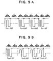
- the 8-16 modulation signal sent from the 8-16 modulator 8 is usually binarized (distinguished between “0" and “1").
- a pulse train waveform for recording the mark portion of a length corresponding to the length of "1" level on the disk 1 is generated on the one hand, and a record waveform for radiating the power level for crystallizing a length corresponding to the length of "0" level (the length of the space portion) is produced on the other hand.
- a pulse train waveform corresponding to the length of each mark portion is stored in a mark table, and a pulse train waveform corresponding to the length of the mark portion is generated.
- the space portion of the disk 1 is irradiated with a beam of a predetermined erase power (second power level).
- the recording of a mark portion requires a mark table describing combinations of the length of a mark portion to be recorded and the length of the space portions before and after the mark portion.
- a mark table describing combinations of the length of a mark portion to be recorded and the length of the space portions before and after the mark portion.
- a pulse train waveform including a pulse of third power level capable of recording a mark portion is generated for the mark portion, and a combination of cooling pulse power and erase power corresponding to the length of each space portion is radiated on the space portion (Fig. 9B).
- a mark table and a space table are arranged in the record waveform generating circuit 6, so that a pulse train waveform corresponding to the length of the mark portion is called from the mark table, and a cooling pulse waveform corresponding to the length of the succeeding space portion is called from the space table.
- the waveforms to be stored in the mark table and the space table can be limited to nine types. Therefore, the record waveform generating circuit can be simplified, thereby contributing to a lower cost of the information recording apparatus. (This system will hereinafter be referred to as "the mark/space independent table system").
- a similar effect of trailing edge jitter suppression is obtained by maintaining the cooling pulse width at a constant level and changing the power level like P4 (3T) or P4 (4T) according to the length of the space portion immediately following the mark portion.
- the power level of the cooling pulse for recording a mark portion followed by a 4T space portion is made minimum.
- the power is changed to the second power level P2.
- the second power level P2 is held, and therefore the area having a recorded mark portion is stably crystallized into the first physical state, thus erasing the information stored therein.
- the distance between a given mark portion and the next mark portion is small, however, e.g. that the space portion is 3T.
- the second power level following the cooling pulse for the preceding mark portion is P2 (3T) which is 0.1 mW to 1.0 mW lower than the second power level for the other mark lengths, residue or shift of the leading edge of the mark portion can be prevented and the jitter of the trailing edge becomes 10%.
- the information recording apparatus can be reduced in cost by providing a mark table and a space table for optimally controlling the power level of the cooling pulse according to the mark/space independent table system.
- a trial write operation (the operation of determining an optimum mark table and an optimum space table for each information recording medium) can be simplified by recording an optimum mark table and an optimum space table in the information recording medium in advance.
- the cooling rate of a rear or trailing part of a mark portion can be controlled by changing the width or level of the low-power part (cooling pulse) following the last pulse of an energy beam pulse train for forming a mark portion and hence by changing the energy radiated on the particular part.
- the shape of the mark portion can thus be optimized.
- the distortion of the reproduced signal is reduced especially to a small value and therefore the system is most suitable for high density recording.
- the product of the time for which the low-power portion is irradiated and the relative speed between the energy beam and the information recording medium is not less than one third of the diameter of the energy beam spot, on the other hand, the erasure by the second power level (crystallization for the phase change record film) may not be sufficiently accomplished.
- Fig. 11 shows an example of a combination of the aforementioned waveform control schemes.
- the energy beam pulse waveforms shown in Fig. 11 have the highest practical value among the embodiments, and can effectively suppress the jitters.
- a jitter value of 9% or less can be obtained by using four power levels including P2, P3, P4 and P5 having the above-mentioned relation.
- Fig. 11 shows only the mark portions having the length of 3T, 4T, 6T, 11T. In the mark portions having the length of 5T to 10T, however, a set of waveforms each having a combination of a high power level pulse and a low power level pulse is added for each T/2 following the first pulse of the 4T waveform.
- the result of adding seven such sets is an energy beam pulse train for recording a mark portion having the length of 11T. Pulses are added similarly also for the mark portions longer than 11T.
- the width of the first pulse is set to 1T, the width of the last pulse to 1T and the width of other pulses to T/2.
- a pulse of preheat level P5 with the duration of 0 to 2T higher than P2 and lower than P3 in power level is arranged immediately before the first pulse of power level P3.
- the width of this pulse of preheat level P3 is changed in accordance with the cooling rate of the medium, the relative speed between the laser beam and the medium, the relation between the radius of the laser beam and the length of the mark portion or the length of the space portion adjacent to a mark portion.
- the conditions for the width and power level of each pulse are shown below. (Power level of pulse train of information pulse section)
- the jitter value is 9% and remains unchanged after overwrite operation.
- the cooling pulse is narrowed by 1T or widened by 1T from the above-mentioned state, noises occur due to a residue at the time of overwrite operation and the jitter value is deteriorated to 15% or more.
- the waveform shown in Fig. 11 is a preferable record waveform especially in that the jitter level is low, the jitter is not increased even after the overwrite operation is repeated, and the record waveform generating circuit can be simplified, as described above.
- Fig. 12 Another example of combinations for waveform control is shown in Fig. 12.
- the relative height between the third, fifth, seventh and ninth power levels is preferably as described below. The relation between the height of power levels and jitters is also described.
- the relative height between the second, fourth, sixth, eighth and tenth power levels is preferably as described below.
- the relative height between the first power level and the fourth, sixth, eighth and tenth power levels is preferably as described below.
- An excessively large circuit size is avoided by assuring that the eighth power level is the same as the tenth power level, and so is by assuring that the seventh power level is the same as the ninth power level. It is also possible to prevent the circuit size from increasing excessively by assuring that at least one of the sixth, eighth and tenth power levels is the same as the fourth power level. Among the sixth, eighth and tenth power levels, an undesirable increase of jitter due to reduction of the circuit structure scale is small when assuring that the tenth power level is the same as the fourth power level.
- the above-mentioned energy beam pulse waveform can reduce the jitter ( ⁇ /Tw) by about 18% as compared with the conventional waveform shown in Fig. 3.
- the size of the record waveform generating circuit is desirably minimized.
- the width of the pulse of the energy beam for forming a mark portion is not necessarily T/2, however, but can be T/3, T/4 or an integral multiple of the channel clock divided by an integer.
- the channel clock is divided by a greater number, the width described above can be desirably optimized for higher accuracy. Excessive division, however, undesirably increases the circuit size. A desirable compromise, therefore, is T/2 to T/4.
- the energy beam pulse waveform according to this embodiment is especially effective when the beam spot diameter (the length along the recording track of the recording medium irradiated with the beam with an intensity at least 1/exp(2) of the intensity at the beam center) is 0.8 ⁇ m to 1.3 ⁇ m and the shortest bit length is 0.25 to 0.35 ⁇ m or the shortest length of the mark portion is in the range of 0.35 ⁇ m to 0.5 ⁇ m. This is by reason of the fact that as described above, depending on the relation between the beam spot and the length of the mark portion, there is a certain range in which the preceding mark portion is liable to be erased (crystallized) by the succeeding pulse as a feature unique to the phase change recording scheme.
- This range is given by the beam diameter and the shortest length of the mark portion.
- the residue in the broad sense of the word has a considerable effect.
- an especially great effect results when the signal modulation scheme of EFM or the 8-16 modulation is employed.
- the range between 630 nm and 670 nm inclusive is especially effective.
- the pulse of each level may develop an overshoot or an undershoot due to the characteristics of an electrical signal. The effect of this invention is not lost as far as an equivalent level is secured in this range.
- an optimum pulse width and an optimum power level are recorded beforehand in a medium as the record waveform information to permit the pulse width of each power level described above to be changed in accordance with the characteristics of the medium, a high-density recording is possible over a very wide range even in the case where the medium cooling rate or the linear velocity for recording (relative speeds of the medium and the laser beam) is changed.
- the waveform of Fig. 5 is optimized and used for recording in a manner similar to that for the waveform of Fig. 4.
- a leading edge jitter value of the signal reproduced from the information recording medium is 11%.
- the result of a similar optimization and recording for the waveforms of Figs. 6 and 7 shows that the jitter values of the signals reproduced from the information recording medium are 9% and 8.5%, respectively.
- the jitter value of the signal reproduced from the lands begins to be affected from the track offset of about 0.05 ⁇ m, and increases to 15% or more when the track offset is 0.10 ⁇ m. This is caused by the phenomenon (what is called the cross erasure) in which the marks recorded on the lands are crystallized by the heat generated when mark portions are recorded in the grooves adjacent to the lands.
- the mark portions are recorded in the adjacent grooves with the energy beam pulse waveform shown in Figs.
- Fig. 13 is a block diagram showing an information recording apparatus according to an embodiment of the invention.
- An information recording medium 1 after being mounted, is rotated by a motor 2 at the rate of 9 m/s with a constant disk linear velocity.
- Information on the recordable disk linear velocity is stored together with the record waveform information in advance in the form of pits in the lead-in area along the innermost circumference of the information recording medium 1.
- the recordable disk linear velocity information read by an optical disk 3 is transferred to a system controller 5 through a pre-amplifier circuit 4.
- information on the record waveform and the optimum recording power are transferred to the system controller 5 through the circuit 4.
- the system controller 5 controls the motor 2 based on the recordable disk linear velocity information and the radial position information of the optical head 3 and rotates the information recording medium 1 at an appropriate rotational speed.
- a record waveform generating circuit 6 has record waveforms (corresponding to, for example, the energy beam pulse waveforms shown in Fig. 12) programmed therein to meet the situation where the time width of the fifth power level, the cooling pulse width and the time width of the third and ninth power levels are 0T, 0.125T, 0.25T, 0.375T, 0.5T, 0.625T, 0.75T, 0.875T, 1.0T, 1.125T, 1.25T, 1.375T, 1.5T, 1.625T, 1.75T, 1.875T, 2.0T, 2.125T, 2.25T, 2.375T and 2.5T.
- the laser driving circuit 7 causes the semiconductor laser in the optical head 3 to emit light, so that the energy beam for recording a mark portion is radiated in a pulse waveform on the information recording medium 1.
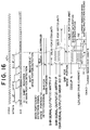
- Fig. 14 is a functional block diagram showing a configuration of the record waveform generating circuit (block 6 in Fig. 13).
- a clock 8fCLK eight times higher in frequency than the channel clock is supplied from a system controller (block 5 in Fig. 13) to the circuit 6.
- a clock 2fCLK twice as high as the channel clock is generated at a 1/4 frequency division counter 6-13.
- a 1/2 frequency division counter 6-14 generates a channel clock CHCLK.
- the recording data input signal WTDATA from the 8-16 modulator 8 is connected to the serial input terminal of a 16-bit shift register 6-1 for input signal, and is shifted at the rise timing of the channel clock CHCLK.
- the 15 bits other than the oldest information bit are applied to a priority encoder 62 for detecting the weight of "1" and an inverted priority encoder 6-3 for detecting the weight of "0".
- the two bits from the oldest information bit side are applied to a decoder 6-4 for detecting the boundary point between a space portion ("0") and a mark portion ("1") and a boundary point changing from a mark portion ("1") to a space portion ("0").
- the numerical value at the point where the output of "1s" to the priority encoder 6-2 is discontinued is stored in a first 4-bit register 6-5.
- the data in a preheat pattern table 6-7 and a mark pattern table 6-8 (which has two 32-bit tables, though not shown) are accessed.
- the data thus accessed are loaded in parallel in output shift registers 6-10, 6-11a, 6-11b at the trailing edge of the mark detection pulse.
- the serial output of the first output shift register 6-10 operated by the clock 8fCLK and the serial output of a second output shift register 6-11a operated by the clock 2fCLK are converted into a first record pulse signal WRTP1-P and a second record pulse signal WTRP2-P through AND gates 6-15 and 6-16, respectively.
- the decoder 6-4 detects the position of change to the space portion (point where "1" changes to "0")
- the numerical value at the point where the "0s" outputted to the inverted priority encoder 6-3 is discontinued is stored in a second 4-bit register 6-6.
- the data retrieved from the cooling pattern table 6-9 are loaded in parallel in a fourth output shift register 6-12.
- a serial output synchronous with the channel clock 3N (8fCLK) eight times higher is converted into an inverted cooling pulse signal COOLP-N through a NOR gate 6-17 and a NAND gate 6-18.
- a write request signal (write gate signal) WRTQ-P generated in the system controller is used as a permission signal for the AND gates 6-15, 6-16 and the NAND gate 6-18, and the serial output of a third output shift register 6-11b is applied as the other input signal to the NOR gate 6-17.
- the above-mentioned three types of bit serial data signals WRTP2-P, WRTP1-P and COOLP-N are supplied to a laser driving circuit (block 7 of Fig. 13, described in detail later) thereby to generate various levels of laser driving signals.
- the contents of the pattern generating tables 6-7, 6-8, 6-9 can be updated from time to time by data transfer from the system control bus 5-1 of the system controller (block 5 of Fig. 13). As a result, it is possible to change the cooling pulse width Tc, etc. (Figs. 11 and 12) as required.
- Fig. 15 is a functional block diagram showing the laser driving circuit (block 7 of Fig. 13).
- This circuit includes an automatic power control (APC) circuit 7-1, three driving current superposition circuits 7-2, 7-3, 7-4 and four D/A converters (DAC) 7-5, 7-6, 7-7, 7-8.
- the output value Vr (target value of the laser power) of the APC D/A converter 7-5 is set by the data transfer from the system control bus 5-1 of the system controller (block 5 of Fig. 13).
- the output current Ir is supplied to the semiconductor laser 3-1 to generate a laser beam, which is partially returned to a monitor photo-diode.
- the resulting voltage is applied through a resistor R2 to an operational amplifier OPA1 and compared with the output voltage Vr of the D/A converter 5.
- the output current Ir is controlled in such a manner that the output voltage of the operational amplifier OPA2 (proportional to the intensity of the laser beam) is balanced with the above-mentioned voltage Vr.
- the loop gain of the APC circuit is determined by the ratio between resistors R2 and R3, and the diode D1 is for blocking the reverse flow of the superposition current (described later).
- the analog switch (ASW) SW1 opens. Therefore, the transistor Q1 turns off and the super-position current ⁇ Im ceases to flow.
- a superposition current ⁇ Ih1 (the superposition current for generating the preheat level power P5. Figs. 1 to 4) flows.
- a superposition current ⁇ Ih2 (the superposition current for generating the laser power of third power level) flows.
- Fig. 16 is a time chart showing the operation described above.
- pulse information "COOLP-N" is obtained from a NOR output of the mark portion cooling signal "MSHR SO-2" and the output of the shift register 6-12 in the NOR gate 6-17 in Fig. 14, pulse information "COOLP-N" is obtained.
- These three laser drive timing signals WRTP2-P, WRTP1-P and COOLP-N are applied to the laser driving circuit shown in Fig. 15, so that a predetermined laser driving current ILD flows to produce a laser beam power as required.
- the laser driving circuit 7 shown in Fig. 15 may be partly changed in such a manner that the used transistors are of NPN type, circuitry for using a negative power supply is added and the above-mentioned space portion cooling pulse signal is applied to the added circuit. Thereby, a current subtraction circuit is formed, which facilitates realization of the waveform indicated by dotted line (laser driving current) shown in Fig. 16.
- Fig. 17 is an I-P (current versus optical beam power) characteristic diagram of a semiconductor laser (3-1 in Fig. 15) according to an embodiment of the invention.
- the laser current is Ir milliamperes
- the laser beam power is Pr milliwatts.
- Superposition of ⁇ Im milliamperes on the current Ir leads to the laser current of Im milliamperes thereby to produce the laser beam power of Pm milliwatts (power level P2).
- Pm milliwatts power level P2 milliwatts
- the laser current of Ih1 milliamperes flows so that the laser beam power assumes Ph1 milliwatts (power level P5).
- the laser current of Ih2 milliamperes flows, with the result that the laser beam power assumes Ph2 milliwatts (power level P3).
- the information recording apparatus comprises a record waveform generating circuit capable of setting and changing the preheat pulse width and the cooling pulse width in units of T/8. Therefore, the requirement of a high disk linear velocity is readily met. Further, a highly accurate information recording becomes possible in an information recording medium having various cooling rates.
- a delay circuit for delaying the trailing edge of a pulse reaching the third power level or the cooling pulse by a predetermined amount can be inserted between the record waveform generating circuit 6 and the laser driving circuit 7 of Fig. 13, for example, in order to adjust the mark portion edge position.
- the method of forming a mark portion of intermediate length by first raising power slightly before raising it to the third power level as between 5T and 7T or by reducing the power following the first record pulse only to a level slightly higher than the first record pulse has the advantage of preventing the temperature drop to the nucleation temperature, thus avoiding the above-mentioned phenomenon.
- the power is lowered for a slightly longer time or to a slightly lower level.
- the last-mentioned method lengthens the actual succeeding space portion and reduces the adverse effect on the resolution of the beam spot especially in the case where the succeeding space portion is short.
- the length of the immediately-succeeding mark portion or space portion is included in the information providing a reference for determining the record waveform of the presently-formed mark portion or space portion. This is effective especially in the high-density recording in which a small residue (a residue in the broad sense of the word, including the effect of a previously-recorded signal pattern on the shape of a new mark portion) has a great effect on the jitter (or shift) at the mark portion edge of the reproduced signal.
- the power level immediately following the first pulse is set to not lower than the power level immediately following each of the other pulses.
- the width of the front part of the mark portion and the width of the rear part of the mark portion can be controlled independently of each other. This method, therefore, is suitable for high-density recording.
- the power level immediately following the first pulse is lower than the power level immediately following each of the other pulses, on the other hand, the energy amount radiated on the front part of the mark portion is insufficient, and therefore the mark portion may assume the form of teardrop.
- the power level of the first pulse is increased as compared with the power level of the last pulse, and the power level immediately following the first pulse is set to not less than the power level immediately following each of the pulses other than the first pulse. In this way, the requirement for a still higher density recording is met.
- Controlling the power level of the first pulse and/or the power level of the pulse immediately following the first pulse is effective for controlling the shape of the front part of the mark portion. An especially great effect is exhibited if this control method is combined with the method of controlling the radiation energy of the cooling pulse effective for controlling the shape of the rear part of the mark portion.
- the width of recrystallized area can be easily controlled by the temperature reached and the cooling rate. Therefore, it is difficult for the mark portion to assume the shape of teardrop or inverse teardrop, thereby making it possible to suppress the size variations of the mark portion to a minimum. Thus, a reproduced signal faithful to the record waveform is produced. Nevertheless, the present invention is applicable also to a recording medium of other characteristics such as the one wholly occupied by large crystal grains.
- the width of the low-power portion after the pulse train of the third power level can be differentiated according to whether the information is recorded in the grooves or on the lands.
- an especially low jitter value is obtained in the case where the energy of the energy beam charged in the first and last pulses is larger than the energy charged in the other pulses.
- This effect is conspicuous at the time of high-speed recording when the disk linear velocity is 9 m/s or more or at the time of high-density recording when the length of the shortest mark portion is not more than two third of the laser beam spot diameter.
- the cooling rate of the record film during and after radiation of the energy beam for forming a mark portion can be accurately controlled. Consequently, a medium capable of phase change between crystal and amorphous states (what is called a phase change recording medium) can be used for high-density recording of information. This is due to the fact that the shape of a mark portion recorded in the phase change recording medium depends very sensitively on the cooling rate of the record film after radiation of the energy beam.
- the width of the pulse in the above-mentioned energy beam pulse train for forming a mark portion or the width of the low-power portion (cooling pulse) following the pulse train represents the time between a local minimum and a local maximum of the differentiation of the temporal change of energy in the energy beam radiated on the information recording medium. More precisely, it represents the time between a local minimum and a local maximum of the time-differentiated signal of an overriding electrical signal (such an electrical signal as digitized for generating a record waveform). In the case where the time between a local minimum and a local maximum is quantized, the width of quantization is called the pulse width described above.
- the time referred to above is of course not the absolute one, but the time relative to the clock of the highest order (the channel clock, i.e. a clock corresponding to the basic clock of the electrical signal immediately after passing an EFM modulator, 8-16 modulator or the like). Therefore, in the case where the channel clock undergoes a change in accordance with the relative speed between the energy beam and the information recording medium, the pulse width described above should be defined taking the relation with the changed channel clock into consideration.
- the power level described above indicates the one assumed to be sustained considerably long time in each pulse (within the time between a local minimum and a local maximum).
- the power level corresponds to the voltage level of an overriding electrical signal (such an electrical signal digitized for generating a record waveform), however, the particular correspondence is taken into account.
- the recording power can be prevented from increasing by recording information using a waveform in which energy is distributed excessively to the leading part and the trailing part of the energy beam pulse train for recording the longest mark portion.
- the power level immediately following the first pulse and the power level immediately before the last pulse are increased as compared with the power level following each of the other pulses.
- the power level immediately following the first pulse is set higher than the power level following each of the pulses other than the first and last pulses but not higher than 200% of the second power level.
- the shortest mark portion is recorded by two energy beam pulses
- the second shortest mark portion is recorded by three energy beam pulses
- the third shortest mark portion is recorded by four energy beam pulses.
- the power level between the first and second pulses for recording the shortest mark portion, the power level between the first and second pulses for recording the second shortest mark portion, the power levels between the first and second pulses and between the third and fourth pulses for recording the third shortest mark portion are set between 50% and 170% inclusive of the second power level.
- the power level between the second and third pulses for recording the second shortest mark portion and the power level between the second and third pulses for recording the third shortest mark portion are set to not more than 50% of the second power level.
- the power level following the first pulse is higher than the power level following each of the pulses other than the first and last pulses but not higher than 200% of the second power level, or more preferably, between 50% and 170% inclusive of the second power level.
- the power level immediately following the first pulse can be set to the second power level.
- a method considered for improving the recording sensitivity other than those mentioned above consists in increasing the width of the first and last pulses in the energy beam pulse train for recording at least the longest mark portion.
- the distance between the first pulse and the last pulse becomes so short that the energy amount radiated per unit area becomes excessive as compared with when recording a comparatively long mark portion such as the longest mark portion, with the result that a comparatively short mark is liable to be long as compared with the normal length.
- At least the power level of the pulse for recording the shortest mark portion is lower than the power level of the second pulse for recording the longest mark portion, and/or: (b) At least the power level of the lowest-power one of the pulses for recording the shortest mark portion is lower than the power level of the second one of the pulses for recording the longest mark portion but not lower than 75% of the power level of the lowest-power one of the pulses for recording the longest mark portion.
- the excessive amount of heat generated for recording the shortest mark portion can be reduced so that a normal length of the shortest mark portion can be secured.
- the excessive heat amount generated for recording the second or third shortest mark portion can be more preferably reduced thereby to secure a normal length of the second or third shortest mark portion, as the case may be.
- the pulse level is increased with the increase of the length of the mark portion to be recorded. Then, the amount of energy radiated per unit area for recording all the mark portions is averaged out, and a normal length can be secured for all the mark portions, thereby making this method more suitable for high-density recording.
- the quality of the reproduced signal is improved and the effect of lowering the power level is exhibited for recording the shortest mark portion as compared with any one of the power levels for recording the longest mark portion, in the case where the power level of the pulse for recording the shortest mark portion is not lower than about 75% of the power level of the lowest-power pulse for recording the longest mark portion.
- An especially great effect is produced when the power level for recording the shortest mark portion is between 85% and 95% inclusive of the power level of the second pulse for recording the longest mark portion.
- the effect of the invention is not produced in the case where the power level for recording the shortest mark portion is lower than 75% of the power level of the second pulse for recording the longest mark portion.
- the width of the first and last pulses reaching the third power level is increased as compared with the width of those other than the first and last pulses reaching the third power level, and at least the power level of the pulse for recording the shortest mark portion is set lower than the power level of the second pulse for recording the longest mark portion.
- the cooling pulse can be arranged after other power levels or, for example, the second power level for a short time, instead of immediately following the last pulse in an energy beam pulse train for recording a mark portion.
Landscapes
- Physics & Mathematics (AREA)
- Optics & Photonics (AREA)
- Optical Recording Or Reproduction (AREA)
- Optical Head (AREA)
Priority Applications (1)
| Application Number | Priority Date | Filing Date | Title |
|---|---|---|---|
| EP02027855A EP1304685A3 (fr) | 1997-09-09 | 1998-09-04 | Méthode et appareil d'enregistrement d'information pour la réduction du sautillement dans les flancs des marques |
Applications Claiming Priority (3)
| Application Number | Priority Date | Filing Date | Title |
|---|---|---|---|
| JP243669/97 | 1997-09-09 | ||
| JP24366997A JP3323782B2 (ja) | 1997-09-09 | 1997-09-09 | 情報の記録方法 |
| JP24366997 | 1997-09-09 |
Related Child Applications (2)
| Application Number | Title | Priority Date | Filing Date |
|---|---|---|---|
| EP02027855A Division EP1304685A3 (fr) | 1997-09-09 | 1998-09-04 | Méthode et appareil d'enregistrement d'information pour la réduction du sautillement dans les flancs des marques |
| EP02027855.2 Division-Into | 2002-12-12 |
Publications (2)
| Publication Number | Publication Date |
|---|---|
| EP0902424A1 true EP0902424A1 (fr) | 1999-03-17 |
| EP0902424B1 EP0902424B1 (fr) | 2003-05-21 |
Family
ID=17107240
Family Applications (2)
| Application Number | Title | Priority Date | Filing Date |
|---|---|---|---|
| EP02027855A Ceased EP1304685A3 (fr) | 1997-09-09 | 1998-09-04 | Méthode et appareil d'enregistrement d'information pour la réduction du sautillement dans les flancs des marques |
| EP98116819A Expired - Lifetime EP0902424B1 (fr) | 1997-09-09 | 1998-09-04 | Méthode d'enregistrement d'information pour la réduction du sautillement sur les bords des marques d' enregistrement |
Family Applications Before (1)
| Application Number | Title | Priority Date | Filing Date |
|---|---|---|---|
| EP02027855A Ceased EP1304685A3 (fr) | 1997-09-09 | 1998-09-04 | Méthode et appareil d'enregistrement d'information pour la réduction du sautillement dans les flancs des marques |
Country Status (5)
| Country | Link |
|---|---|
| US (14) | US6236635B1 (fr) |
| EP (2) | EP1304685A3 (fr) |
| JP (1) | JP3323782B2 (fr) |
| KR (2) | KR100426235B1 (fr) |
| DE (1) | DE69814773T2 (fr) |
Cited By (18)
| Publication number | Priority date | Publication date | Assignee | Title |
|---|---|---|---|---|
| WO2000060584A1 (fr) * | 1999-03-30 | 2000-10-12 | Koninklijke Philips Electronics N.V. | Procede et dispositif d'enregistrement de marques dans une couche d'information d'un support d'enregistrement optique |
| EP1045378A2 (fr) * | 1999-04-13 | 2000-10-18 | Hitachi, Ltd. | Méthode et appareil d'enregistrement d'informations |
| WO2000072316A1 (fr) * | 1999-05-19 | 2000-11-30 | Mitsubishi Chemical Corporation | Procede d'enregistrement optique et support d'enregistrement optique |
| EP1058240A2 (fr) | 1999-06-03 | 2000-12-06 | Samsung Electronics Co., Ltd. | Procédé de génération de signaux de commande pour impulsions d'écriture pour supports d'enregistrement optique et appareil d'enregistrement utilisant ce procédé |
| EP1061509A2 (fr) * | 1999-06-18 | 2000-12-20 | Samsung Electronics Co., Ltd. | Procédé et dispositif d'enregistrement auto-adaptif pour un appareil d'enregistrement optique haute densité, et procédé de commande associé |
| WO2001004885A1 (fr) * | 1999-07-07 | 2001-01-18 | Koninklijke Philips Electronics N.V. | Procede et dispositif d'ecriture de marques sur une couche d'information d'un support d'enregistrement optique |
| WO2001078072A1 (fr) * | 2000-04-07 | 2001-10-18 | Matsushita Electric Industrial Co., Ltd. | Procede d'enregistrement/reproduction de donnees sur/depuis un disque optique |
| EP1207525A2 (fr) * | 2000-11-15 | 2002-05-22 | Ricoh Company, Ltd. | Procédé d'enregistrement optique d'informations avec un schéma amélioré pour la commande de la puissance d'enregistrement |
| WO2003046896A2 (fr) * | 2001-11-28 | 2003-06-05 | Koninklijke Philips Electronics N.V. | Procede et dispositifs pour l'enregistrement de reperes dans une couche d'enregistrement d'un support optique |
| WO2003073419A1 (fr) * | 2002-02-28 | 2003-09-04 | Tdk Corporation | Procede d'enregistrement d'informations sur support d'enregistrement optique, enregistreur d'informations et support d'enregistrement optique |
| WO2003030153A3 (fr) * | 2001-09-27 | 2003-10-02 | Koninkl Philips Electronics Nv | Procede et dispositif d'enregistrement permettant de choisir une strategie d'ecriture optimisee et support d'enregistrement utilise avec ce procede |
| WO2004029944A1 (fr) | 2002-09-30 | 2004-04-08 | Nec Corporation | Procede de fixation de parametre d'enregistrement et enregistreur de donnees utilisant celui-ci |
| EP1467353A1 (fr) * | 2002-01-16 | 2004-10-13 | TDK Corporation | Procede d'enregistrement d'informations sur un support d'enregistrement optique, support d'enregistrement optique et enregistreur/lecteur |
| SG113432A1 (en) * | 1999-07-15 | 2005-08-29 | Koninkl Philips Electronics Nv | Method and device for recording marks in an information layer of an optical record carrier, and record carrier for use therein |
| EP1635337A1 (fr) * | 2003-06-13 | 2006-03-15 | Ricoh Company, Ltd. | Procede d'enregistrement de donnees et dispositif d'enregistrement de donnees |
| EP1482486A3 (fr) * | 2003-05-27 | 2007-06-27 | Matsushita Electric Industrial Co., Ltd. | Procédé d'enregistrement optique d'informations, dispositif d'enregistrement optique d'informations et support d'enregistrement optique d'informations |
| US7313070B2 (en) | 2002-02-13 | 2007-12-25 | Mitsubishi Kagaku Media Co., Ltd. | Rewritable optical recording medium and optical recording method |
| US7443776B2 (en) | 2002-12-13 | 2008-10-28 | Mitsubishi Kagaku Media Co., Ltd. | Optical recording method |
Families Citing this family (69)
| Publication number | Priority date | Publication date | Assignee | Title |
|---|---|---|---|---|
| JP3323782B2 (ja) * | 1997-09-09 | 2002-09-09 | 株式会社日立製作所 | 情報の記録方法 |
| JP2000123367A (ja) * | 1998-10-14 | 2000-04-28 | Toshiba Corp | 相変化光記録媒体の記録方法及び記録装置 |
| US7272094B2 (en) * | 1999-07-15 | 2007-09-18 | Koninklike Philips Electronics N.V. | Methods and devices for recording marks in an information layer of an optical record carrier, and record carriers for use therein |
| US7212477B2 (en) * | 1999-07-23 | 2007-05-01 | Ricoh Company, Ltd. | Optical recording/reproducing apparatus with APC and SPS processes |
| JP2001067669A (ja) * | 1999-08-31 | 2001-03-16 | Sony Corp | 記録装置、記録方法 |
| JP3839213B2 (ja) * | 2000-02-08 | 2006-11-01 | 株式会社リコー | 相変化型光記録媒体の記録方法および記録再生装置 |
| JP2002008237A (ja) * | 2000-06-23 | 2002-01-11 | Fujitsu Ltd | 情報記録方法及びその実施に使用する情報記録装置 |
| US6396793B1 (en) * | 2000-08-30 | 2002-05-28 | Eastman Kodak Company | Preheating beams for optical recording |
| KR100403614B1 (ko) * | 2000-11-29 | 2003-11-01 | 삼성전자주식회사 | 고밀도 광기록을 위한 적응적 기록 제어 방법 |
| JP3921046B2 (ja) * | 2000-12-07 | 2007-05-30 | 株式会社日立製作所 | 情報記録方法及び光ディスク装置 |
| JP4491985B2 (ja) * | 2001-03-28 | 2010-06-30 | Tdk株式会社 | 光記録方法 |
| US6699557B2 (en) * | 2001-03-30 | 2004-03-02 | Tdk Corporation | Optical recording medium and optical recording method |
| JP4814476B2 (ja) * | 2001-04-20 | 2011-11-16 | Tdk株式会社 | 光情報媒体の再生方法 |
| US7864645B2 (en) * | 2001-04-26 | 2011-01-04 | Koninklijke Philips Electronics N.V. | Method and device for recording marks in an information layer of an optical record carrier |
| US7123569B2 (en) * | 2001-09-04 | 2006-10-17 | Imation Corp. | Optical data storage medium |
| TWI261236B (en) * | 2001-09-29 | 2006-09-01 | Samsung Electronics Co Ltd | Method for forming first state and second state on optical recording medium |
| CN1248201C (zh) * | 2001-10-02 | 2006-03-29 | 松下电器产业株式会社 | 光学信息记录方法以及再生装置 |
| JP2003123252A (ja) * | 2001-10-09 | 2003-04-25 | Hitachi Ltd | 情報記録方法および情報記録装置 |
| JP3740413B2 (ja) * | 2001-12-20 | 2006-02-01 | 株式会社日立製作所 | 高周波重畳方法およびこれを用いた光ディスク装置 |
| JP2003242644A (ja) | 2002-02-14 | 2003-08-29 | Tdk Corp | 光記録媒体への情報記録方法、情報記録装置及び光記録媒体 |
| KR100459702B1 (ko) | 2002-02-22 | 2004-12-04 | 삼성전자주식회사 | 광 구동기에 있어서 기록 광 파워 제어장치 및 방법 |
| US7376064B2 (en) | 2002-02-25 | 2008-05-20 | Samsung Electronics Co., Ltd. | Method and apparatus for recording data on optical recording medium |
| US7106680B2 (en) * | 2002-05-10 | 2006-09-12 | Ricoh Company, Ltd. | Device and method for recording data to optical disk using multi-pulse to enhance power pulse |
| JP3851886B2 (ja) * | 2002-05-27 | 2006-11-29 | パイオニア株式会社 | 情報記録装置および情報記録方法 |
| JP3954438B2 (ja) * | 2002-05-31 | 2007-08-08 | Tdk株式会社 | 光記録媒体への情報記録方法、情報記録装置及び光記録媒体 |
| KR100911140B1 (ko) | 2002-06-03 | 2009-08-06 | 삼성전자주식회사 | 광 기록매체에 데이터를 기록하는 방법 및 그 장치 |
| US7260044B2 (en) * | 2002-09-06 | 2007-08-21 | Ricoh Company, Ltd. | Recording method for a phase-change optical recording medium |
| EP1699044B1 (fr) * | 2002-10-10 | 2007-10-24 | Matsushita Electric Industrial Co., Ltd. | Procédé et appareil d'enregistrement d'enregistrement optique de données |
| JP2004206739A (ja) * | 2002-11-06 | 2004-07-22 | Ricoh Co Ltd | 情報記録方法及び情報記録装置 |
| JP2004171642A (ja) * | 2002-11-19 | 2004-06-17 | Tdk Corp | 光記録媒体、光記録方法及び光記録装置 |
| TWI261825B (en) * | 2002-12-16 | 2006-09-11 | Hitachi Maxell | Data recording method and data recording medium |
| CN1328719C (zh) * | 2002-12-30 | 2007-07-25 | 皇家飞利浦电子股份有限公司 | 耗散低功率的信息记录设备 |
| JP4272892B2 (ja) * | 2003-01-08 | 2009-06-03 | 富士フイルム株式会社 | 信号出力方法 |
| JP2006513522A (ja) * | 2003-01-23 | 2006-04-20 | サムスン エレクトロニクス カンパニー リミテッド | 光記録媒体、それにデータを記録する方法及びその装置 |
| JP4123007B2 (ja) * | 2003-02-27 | 2008-07-23 | ヤマハ株式会社 | 光ディスク記録方法およびその装置 |
| JP4231871B2 (ja) * | 2003-02-28 | 2009-03-04 | パイオニア株式会社 | 情報記録装置及び情報記録方法 |
| KR100687997B1 (ko) * | 2003-04-04 | 2007-02-27 | 마츠시타 덴끼 산교 가부시키가이샤 | 기록 매체로의 데이터 기록 방법 및 장치 |
| TW200509104A (en) | 2003-05-23 | 2005-03-01 | Matsushita Electric Ind Co Ltd | Information recording medium; recording device, method and program thereof |
| DE602004014378D1 (de) * | 2003-06-26 | 2008-07-24 | Koninkl Philips Electronics Nv | Phasenwechselaufzeichnungsmedium welches bei geringer geschwindigkeit löschbar und bei hoher geschwindigkeit beschreibbar ist und gerät zur verwendung eines solchen mediums |
| US8483717B2 (en) | 2003-06-27 | 2013-07-09 | Qualcomm Incorporated | Local area network assisted positioning |
| US8971913B2 (en) | 2003-06-27 | 2015-03-03 | Qualcomm Incorporated | Method and apparatus for wireless network hybrid positioning |
| JP3998643B2 (ja) * | 2003-06-30 | 2007-10-31 | 東芝マイクロエレクトロニクス株式会社 | レーザ制御装置及び光ディスク装置 |
| JP2005038559A (ja) * | 2003-07-18 | 2005-02-10 | Sony Corp | 情報記録装置及び方法 |
| JP4397751B2 (ja) | 2003-07-18 | 2010-01-13 | 三菱化学メディア株式会社 | 光記録方法及び光記録装置 |
| JP2005063586A (ja) * | 2003-08-18 | 2005-03-10 | Ricoh Co Ltd | 光情報記録方法及び光情報記録装置 |
| JP2005071515A (ja) * | 2003-08-27 | 2005-03-17 | Tdk Corp | 光記録ディスクへのデータ記録方法および光記録ディスクへのデータ記録装置 |
| WO2005027103A1 (fr) * | 2003-09-16 | 2005-03-24 | Lg Electronics Inc. | Procede d'enregistrement pour disque optique a changement de phase |
| KR100997481B1 (ko) * | 2003-09-16 | 2010-11-30 | 엘지전자 주식회사 | 상변화 광디스크의 기록 펄스 파형 조절장치 및 방법 |
| US7606126B2 (en) * | 2003-09-18 | 2009-10-20 | Mitsubishi Kagaku Media Co., Ltd. | Information recording method and information recording medium |
| JP2007507823A (ja) * | 2003-10-03 | 2007-03-29 | コーニンクレッカ フィリップス エレクトロニクス エヌ ヴィ | 記録担体、並びに記録担体を走査する装置及び方法 |
| EP1675107A4 (fr) | 2003-10-17 | 2009-02-18 | Mitsubishi Kagaku Media Co Ltd | Procede d'enregistrement optique |
| JP4216204B2 (ja) | 2004-01-30 | 2009-01-28 | シャープ株式会社 | 光記録条件設定方法、光記録再生装置、制御プログラム、及び記録媒体 |
| JP4179994B2 (ja) * | 2004-02-05 | 2008-11-12 | Tdk株式会社 | 光記録媒体への情報記録方法及び情報記録装置 |
| KR20060132784A (ko) * | 2004-03-30 | 2006-12-22 | 마쯔시다덴기산교 가부시키가이샤 | 정보 기록 방법, 정보 기록 장치 및 정보 기록 매체 |
| US7319878B2 (en) | 2004-06-18 | 2008-01-15 | Qualcomm Incorporated | Method and apparatus for determining location of a base station using a plurality of mobile stations in a wireless mobile network |
| WO2006051654A1 (fr) * | 2004-11-11 | 2006-05-18 | Matsushita Electric Industrial Co., Ltd. | Circuit de correction d’écriture et méthode de génération de signal de correction d’écriture |
| US7701828B2 (en) * | 2005-02-04 | 2010-04-20 | Mediatek Inc. | Optical recording system and method |
| EP1688930A1 (fr) * | 2005-02-08 | 2006-08-09 | Ricoh Company, Ltd. | Support de DVD enregistrable à base de colorants, et procédé et appareil d'enregistrement et de lecture dudit support |
| JP2006309855A (ja) * | 2005-04-27 | 2006-11-09 | Tdk Corp | 光記録媒体への情報記録方法 |
| US7257413B2 (en) * | 2005-08-24 | 2007-08-14 | Qualcomm Incorporated | Dynamic location almanac for wireless base stations |
| US9042917B2 (en) * | 2005-11-07 | 2015-05-26 | Qualcomm Incorporated | Positioning for WLANS and other wireless networks |
| JP2007323719A (ja) * | 2006-05-31 | 2007-12-13 | Toshiba Corp | 光ディスク、情報記録方法、情報再生方法 |
| JP2007323774A (ja) * | 2006-06-02 | 2007-12-13 | Toshiba Corp | 光記録媒体、情報記録方法、情報再生方法 |
| US9226257B2 (en) | 2006-11-04 | 2015-12-29 | Qualcomm Incorporated | Positioning for WLANs and other wireless networks |
| JP2008310922A (ja) | 2007-06-18 | 2008-12-25 | Toshiba Corp | 情報記録媒体及びこの媒体を用いたディスク装置 |
| JP2009238285A (ja) * | 2008-03-26 | 2009-10-15 | Sony Corp | 光記録方法及び光記録装置 |
| US8897801B2 (en) | 2008-06-13 | 2014-11-25 | Qualcomm Incorporated | Transmission of location information by a transmitter as an aid to location services |
| JP5397412B2 (ja) * | 2011-05-20 | 2014-01-22 | 船井電機株式会社 | 光ディスク記録装置及び光ディスク記録方法 |
| US9502068B1 (en) * | 2015-04-08 | 2016-11-22 | Western Digital Technologies, Inc. | Data storage device updating laser power during non-write mode for heat assisted magnetic recording |
Citations (4)
| Publication number | Priority date | Publication date | Assignee | Title |
|---|---|---|---|---|
| DE3804240A1 (de) * | 1987-02-12 | 1988-08-25 | Hitachi Ltd | Verfahren und vorrichtung zur optischen informationsaufzeichnung |
| US5457666A (en) * | 1992-09-07 | 1995-10-10 | Hitachi, Ltd. | Light modulation method for forming a mark in magneto-optical recording system |
| EP0802531A2 (fr) * | 1996-04-17 | 1997-10-22 | Hitachi, Ltd. | Appareil et méthode d'enregistrement d'information |
| EP0851413A2 (fr) * | 1996-12-26 | 1998-07-01 | Hitachi, Ltd. | Appareil d'enregistrement d'informations |
Family Cites Families (28)
| Publication number | Priority date | Publication date | Assignee | Title |
|---|---|---|---|---|
| JP3124720B2 (ja) * | 1995-04-14 | 2001-01-15 | 株式会社リコー | 情報記録再生方法、情報記録再生装置及び情報記録媒体 |
| JP2521908B2 (ja) | 1985-06-11 | 1996-08-07 | 株式会社ニコン | オ―バ―ライト可能な光磁気記録方法、それに使用される光磁気記録装置及び光磁気記録媒体、並びに変調方法、変調装置及び光磁気記録媒体 |
| US5528564A (en) * | 1986-03-07 | 1996-06-18 | Movid Information Technology, Inc. | Direct overwrite magneto-optic system for strip erasing and recording elongated domains |
| JP2719130B2 (ja) | 1986-05-02 | 1998-02-25 | 株式会社日立製作所 | 情報の記録・再生および書き換え方法とその装置 |
| US4939717A (en) | 1986-10-31 | 1990-07-03 | Matsushita Electric Industrial Co., Ltd. | Method and apparatus for erasing and recording information using three power levels |
| US4894846A (en) * | 1988-06-30 | 1990-01-16 | Digital Equipment Corporation | Method for maintaining a correct time in a distributed processing system |
| US5150351A (en) | 1989-06-30 | 1992-09-22 | Matsushita Electric Industrial Co., Ltd. | Optical information recording apparatus for recording an input signal having variable width pulse duration and pulse spacing periods |
| JP2804806B2 (ja) | 1989-12-13 | 1998-09-30 | 株式会社日立製作所 | 情報の記録方法 |
| US5590111A (en) * | 1990-06-29 | 1996-12-31 | Hitachi, Ltd. | Method of controlling recording of optical records |
| JPH05143993A (ja) | 1991-11-18 | 1993-06-11 | Olympus Optical Co Ltd | 光学式情報記録方法 |
| JPH05217236A (ja) * | 1992-02-05 | 1993-08-27 | Sony Corp | 光磁気記録方法 |
| JPH06203383A (ja) | 1992-10-20 | 1994-07-22 | Nikon Corp | 光記録の熱遮断条件決定方法、同決定装置、 光記録方法及び光記録装置 |
| JP2684952B2 (ja) | 1993-04-07 | 1997-12-03 | 松下電器産業株式会社 | ディスク記録方法およびディスク記録装置 |
| JPH08180414A (ja) * | 1994-12-21 | 1996-07-12 | Mitsubishi Chem Corp | 光学的情報記録方法 |
| JP3185629B2 (ja) | 1995-02-09 | 2001-07-11 | 日本鋼管株式会社 | 圧延機および圧延方法 |
| JP3138610B2 (ja) * | 1995-04-13 | 2001-02-26 | 株式会社リコー | 相変化型光ディスク用記録方法 |
| JPH0969246A (ja) * | 1995-08-30 | 1997-03-11 | Canon Inc | 光学的情報記録再生装置 |
| JP3264805B2 (ja) * | 1995-10-16 | 2002-03-11 | 株式会社リコー | 情報記録方式 |
| US5732062A (en) * | 1995-10-16 | 1998-03-24 | Ricoh Company, Ltd. | Information recording apparatus, method and computer program product |
| US5742566A (en) * | 1995-11-27 | 1998-04-21 | Sony Corporation | Optical recording methods and apparatus using light modulation technique based on detecting temperature of the medium |
| AU1614797A (en) * | 1996-02-16 | 1997-09-02 | Philips Electronics N.V. | Method and device for recording an optical information carrier |
| JP3323782B2 (ja) * | 1997-09-09 | 2002-09-09 | 株式会社日立製作所 | 情報の記録方法 |
| TW468177B (en) * | 1998-08-04 | 2001-12-11 | Hitachi Ltd | Data storage method, data storage medium and data storage recording device |
| US20050182735A1 (en) * | 2004-02-12 | 2005-08-18 | Zager Robert P. | Method and apparatus for implementing a micropayment system to control e-mail spam |
| US8073910B2 (en) * | 2005-03-03 | 2011-12-06 | Iconix, Inc. | User interface for email inbox to call attention differently to different classes of email |
| US20070061567A1 (en) * | 2005-09-10 | 2007-03-15 | Glen Day | Digital information protection system |
| EP2359576B1 (fr) * | 2008-11-20 | 2017-12-27 | Mark Kevin Shull | Mecanisme d'authentification par domaine |
| US20110055911A1 (en) * | 2009-08-28 | 2011-03-03 | The Go Daddy Group, Inc. | Business validation based social website account authentication |
-
1997
- 1997-09-09 JP JP24366997A patent/JP3323782B2/ja not_active Expired - Lifetime
-
1998
- 1998-09-04 DE DE69814773T patent/DE69814773T2/de not_active Expired - Lifetime
- 1998-09-04 KR KR10-1998-0036468A patent/KR100426235B1/ko not_active IP Right Cessation
- 1998-09-04 EP EP02027855A patent/EP1304685A3/fr not_active Ceased
- 1998-09-04 EP EP98116819A patent/EP0902424B1/fr not_active Expired - Lifetime
- 1998-09-08 US US09/149,051 patent/US6236635B1/en not_active Expired - Lifetime
-
2001
- 2001-02-02 US US09/773,557 patent/US6343056B2/en not_active Expired - Fee Related
- 2001-05-22 KR KR10-2001-0027957A patent/KR100467917B1/ko not_active IP Right Cessation
- 2001-12-21 US US10/023,719 patent/US6529467B2/en not_active Expired - Lifetime
-
2002
- 2002-10-16 US US10/270,543 patent/US6608806B2/en not_active Expired - Lifetime
-
2003
- 2003-06-23 US US10/600,442 patent/US6842415B2/en not_active Expired - Lifetime
-
2004
- 2004-11-03 US US10/979,125 patent/US7012871B2/en not_active Expired - Lifetime
-
2005
- 2005-06-30 US US11/170,154 patent/US7417933B2/en not_active Expired - Fee Related
- 2005-06-30 US US11/170,155 patent/US7042823B2/en not_active Expired - Lifetime
-
2008
- 2008-03-28 US US12/078,227 patent/US7852727B2/en not_active Expired - Fee Related
- 2008-03-28 US US12/078,219 patent/US20080192617A1/en not_active Abandoned
- 2008-03-28 US US12/078,221 patent/US7684301B2/en not_active Expired - Fee Related
- 2008-07-21 US US12/219,347 patent/US7907491B2/en not_active Expired - Fee Related
- 2008-07-21 US US12/219,346 patent/US7911910B2/en not_active Expired - Fee Related
- 2008-07-21 US US12/219,334 patent/US7907490B2/en not_active Expired - Fee Related
Patent Citations (4)
| Publication number | Priority date | Publication date | Assignee | Title |
|---|---|---|---|---|
| DE3804240A1 (de) * | 1987-02-12 | 1988-08-25 | Hitachi Ltd | Verfahren und vorrichtung zur optischen informationsaufzeichnung |
| US5457666A (en) * | 1992-09-07 | 1995-10-10 | Hitachi, Ltd. | Light modulation method for forming a mark in magneto-optical recording system |
| EP0802531A2 (fr) * | 1996-04-17 | 1997-10-22 | Hitachi, Ltd. | Appareil et méthode d'enregistrement d'information |
| EP0851413A2 (fr) * | 1996-12-26 | 1998-07-01 | Hitachi, Ltd. | Appareil d'enregistrement d'informations |
Cited By (50)
| Publication number | Priority date | Publication date | Assignee | Title |
|---|---|---|---|---|
| WO2000060584A1 (fr) * | 1999-03-30 | 2000-10-12 | Koninklijke Philips Electronics N.V. | Procede et dispositif d'enregistrement de marques dans une couche d'information d'un support d'enregistrement optique |
| EP1045378A3 (fr) * | 1999-04-13 | 2002-02-13 | Hitachi, Ltd. | Méthode et appareil d'enregistrement d'informations |
| EP1045378A2 (fr) * | 1999-04-13 | 2000-10-18 | Hitachi, Ltd. | Méthode et appareil d'enregistrement d'informations |
| US7609602B2 (en) | 1999-04-13 | 2009-10-27 | Hitachi, Ltd. | Method of generating a recording pulse train in accordance with a NRZI signal for recording information to a recording medium |
| US6678228B1 (en) | 1999-04-13 | 2004-01-13 | Hitachi, Ltd. | Method and apparatus for recording information in which the average power of a pulse is adjusted according to control data |
| SG97882A1 (en) * | 1999-04-13 | 2003-08-20 | Hitachi Ltd | Method of and apparatus for recording information |
| US7009923B2 (en) | 1999-04-13 | 2006-03-07 | Hitachi, Ltd. | Method of and apparatus for recording information |
| US6411579B2 (en) | 1999-05-19 | 2002-06-25 | Mitsubishi Chemical Corporation | Optical recording method and optical recording medium |
| EP1372146A2 (fr) * | 1999-05-19 | 2003-12-17 | Mitsubishi Chemical Corporation | Méthode d'enregistrement optique et milieu d'enregistrement |
| US7085215B2 (en) | 1999-05-19 | 2006-08-01 | Mitsubishi Kagaku Media Co., Ltd. | Optical recording method and optical recording medium |
| EP1372146A3 (fr) * | 1999-05-19 | 2004-04-28 | Mitsubishi Chemical Corporation | Méthode d'enregistrement optique et milieu d'enregistrement |
| EP1182649A1 (fr) * | 1999-05-19 | 2002-02-27 | Mitsubishi Chemical Corporation | Procede d'enregistrement optique et support d'enregistrement optique |
| EP1182649A4 (fr) * | 1999-05-19 | 2003-01-22 | Mitsubishi Chem Corp | Procede d'enregistrement optique et support d'enregistrement optique |
| USRE45001E1 (en) | 1999-05-19 | 2014-07-08 | Mitsubishi Kagaku Media Co., Ltd. | Optical recording method and optical recording medium |
| US7050377B1 (en) | 1999-05-19 | 2006-05-23 | Mitsubishi Chemical Corporation | Optical recording method and optical recording medium |
| USRE42786E1 (en) | 1999-05-19 | 2011-10-04 | Mitsubishi Kagaku Media Co., Ltd. | Optical recording method and optical recording medium |
| WO2000072316A1 (fr) * | 1999-05-19 | 2000-11-30 | Mitsubishi Chemical Corporation | Procede d'enregistrement optique et support d'enregistrement optique |
| US6661760B2 (en) | 1999-05-19 | 2003-12-09 | Mitsubishi Chemical Corporation | Optical recording method and optical recording medium |
| EP1058240A2 (fr) | 1999-06-03 | 2000-12-06 | Samsung Electronics Co., Ltd. | Procédé de génération de signaux de commande pour impulsions d'écriture pour supports d'enregistrement optique et appareil d'enregistrement utilisant ce procédé |
| EP1061509A3 (fr) * | 1999-06-18 | 2003-01-15 | Samsung Electronics Co., Ltd. | Procédé et dispositif d'enregistrement auto-adaptif pour un appareil d'enregistrement optique haute densité, et procédé de commande associé |
| US6661759B1 (en) | 1999-06-18 | 2003-12-09 | Samsung Electronics Co., Ltd. | Adaptive recording method and apparatus for high-density optical recording, and control method therefor |
| EP1061509A2 (fr) * | 1999-06-18 | 2000-12-20 | Samsung Electronics Co., Ltd. | Procédé et dispositif d'enregistrement auto-adaptif pour un appareil d'enregistrement optique haute densité, et procédé de commande associé |
| US6781936B1 (en) | 1999-07-07 | 2004-08-24 | Koninklijke Philips Electronics N.V. | Method and device for recording marks in an information layer of an optical record carrier |
| WO2001004885A1 (fr) * | 1999-07-07 | 2001-01-18 | Koninklijke Philips Electronics N.V. | Procede et dispositif d'ecriture de marques sur une couche d'information d'un support d'enregistrement optique |
| SG113432A1 (en) * | 1999-07-15 | 2005-08-29 | Koninkl Philips Electronics Nv | Method and device for recording marks in an information layer of an optical record carrier, and record carrier for use therein |
| CN1324573C (zh) * | 2000-04-07 | 2007-07-04 | 松下电器产业株式会社 | 用于在光盘上记录数据/从光盘再现数据的方法 |
| US6894965B2 (en) | 2000-04-07 | 2005-05-17 | Matsushita Electric Industrial Co., Ltd. | Method for recording/reproducing data on/from optical disk |
| WO2001078072A1 (fr) * | 2000-04-07 | 2001-10-18 | Matsushita Electric Industrial Co., Ltd. | Procede d'enregistrement/reproduction de donnees sur/depuis un disque optique |
| US7019273B2 (en) | 2000-11-15 | 2006-03-28 | Ricoh Company, Ltd. | Optical information recording employing improved recording power control scheme |
| EP1207525A3 (fr) * | 2000-11-15 | 2005-03-09 | Ricoh Company, Ltd. | Procédé d'enregistrement optique d'informations avec un schéma amélioré pour la commande de la puissance d'enregistrement |
| EP1207525A2 (fr) * | 2000-11-15 | 2002-05-22 | Ricoh Company, Ltd. | Procédé d'enregistrement optique d'informations avec un schéma amélioré pour la commande de la puissance d'enregistrement |
| WO2003030153A3 (fr) * | 2001-09-27 | 2003-10-02 | Koninkl Philips Electronics Nv | Procede et dispositif d'enregistrement permettant de choisir une strategie d'ecriture optimisee et support d'enregistrement utilise avec ce procede |
| WO2003046896A3 (fr) * | 2001-11-28 | 2004-07-29 | Koninkl Philips Electronics Nv | Procede et dispositifs pour l'enregistrement de reperes dans une couche d'enregistrement d'un support optique |
| WO2003046896A2 (fr) * | 2001-11-28 | 2003-06-05 | Koninklijke Philips Electronics N.V. | Procede et dispositifs pour l'enregistrement de reperes dans une couche d'enregistrement d'un support optique |
| EP1467353A1 (fr) * | 2002-01-16 | 2004-10-13 | TDK Corporation | Procede d'enregistrement d'informations sur un support d'enregistrement optique, support d'enregistrement optique et enregistreur/lecteur |
| EP1467353A4 (fr) * | 2002-01-16 | 2008-12-03 | Tdk Corp | Procede d'enregistrement d'informations sur un support d'enregistrement optique, support d'enregistrement optique et enregistreur/lecteur |
| US7313070B2 (en) | 2002-02-13 | 2007-12-25 | Mitsubishi Kagaku Media Co., Ltd. | Rewritable optical recording medium and optical recording method |
| US7858167B2 (en) | 2002-02-13 | 2010-12-28 | Mitsubishi Kagaku Media Co., Ltd. | Rewritable optical recording medium and optical recording method |
| US7609603B2 (en) | 2002-02-13 | 2009-10-27 | Mitsubishi Kagaku Media Co., Ltd. | Rewritable optical recording medium and optical recording method |
| US7408860B2 (en) | 2002-02-28 | 2008-08-05 | Tdk Corporation | Method of recording information in optical recording medium, information recording apparatus and optical recording medium |
| WO2003073419A1 (fr) * | 2002-02-28 | 2003-09-04 | Tdk Corporation | Procede d'enregistrement d'informations sur support d'enregistrement optique, enregistreur d'informations et support d'enregistrement optique |
| WO2004029944A1 (fr) | 2002-09-30 | 2004-04-08 | Nec Corporation | Procede de fixation de parametre d'enregistrement et enregistreur de donnees utilisant celui-ci |
| EP1548711A1 (fr) * | 2002-09-30 | 2005-06-29 | NEC Corporation | Procede de fixation de parametre d'enregistrement et enregistreur de donnees utilisant celui-ci |
| EP1548711A4 (fr) * | 2002-09-30 | 2009-01-21 | Nec Corp | Procede de fixation de parametre d'enregistrement et enregistreur de donnees utilisant celui-ci |
| US7443776B2 (en) | 2002-12-13 | 2008-10-28 | Mitsubishi Kagaku Media Co., Ltd. | Optical recording method |
| US7532555B2 (en) | 2002-12-13 | 2009-05-12 | Mitsubishi Kagaku Media Co., Ltd. | Phase-change recording layer optical recording method |
| US7450480B2 (en) | 2003-05-27 | 2008-11-11 | Panasonic Corporation | Optical information recording method, optical information recording device and optical information recording medium |
| EP1482486A3 (fr) * | 2003-05-27 | 2007-06-27 | Matsushita Electric Industrial Co., Ltd. | Procédé d'enregistrement optique d'informations, dispositif d'enregistrement optique d'informations et support d'enregistrement optique d'informations |
| EP1635337A4 (fr) * | 2003-06-13 | 2009-04-01 | Ricoh Kk | Procede d'enregistrement de donnees et dispositif d'enregistrement de donnees |
| EP1635337A1 (fr) * | 2003-06-13 | 2006-03-15 | Ricoh Company, Ltd. | Procede d'enregistrement de donnees et dispositif d'enregistrement de donnees |
Also Published As
Similar Documents
| Publication | Publication Date | Title |
|---|---|---|
| EP0902424B1 (fr) | Méthode d'enregistrement d'information pour la réduction du sautillement sur les bords des marques d' enregistrement | |
| US5802032A (en) | Method and device for recording a mark having a substantially constant number of pulses per unit length independent of writing speed on an optical information carrier | |
| KR101088982B1 (ko) | 기록 방법, 데이터 기록 매체, 재생 방법 및 제조 설비 | |
| EP0802531A2 (fr) | Appareil et méthode d'enregistrement d'information | |
| EP1347444B1 (fr) | Procédé et appareil d'enregistrement de données sur un support d'enregistrement optique | |
| JP3635783B2 (ja) | 情報記録方法及び情報記録装置 | |
| JP3452050B2 (ja) | 情報の記録方法 | |
| JPH1083553A (ja) | 情報記録方法及び情報記録装置 | |
| JP2000076683A (ja) | 情報記録方法及び情報記録装置 |
Legal Events
| Date | Code | Title | Description |
|---|---|---|---|
| PUAI | Public reference made under article 153(3) epc to a published international application that has entered the european phase |
Free format text: ORIGINAL CODE: 0009012 |
|
| AK | Designated contracting states |
Kind code of ref document: A1 Designated state(s): DE FR GB |
|
| AX | Request for extension of the european patent |
Free format text: AL;LT;LV;MK;RO;SI |
|
| 17P | Request for examination filed |
Effective date: 19990409 |
|
| AKX | Designation fees paid |
Free format text: DE FR GB |
|
| 17Q | First examination report despatched |
Effective date: 20020806 |
|
| GRAH | Despatch of communication of intention to grant a patent |
Free format text: ORIGINAL CODE: EPIDOS IGRA |
|
| RTI1 | Title (correction) |
Free format text: INFORMATION RECORDING METHOD WITH SUPPRESSED MARK EDGE JITTERS |
|
| GRAH | Despatch of communication of intention to grant a patent |
Free format text: ORIGINAL CODE: EPIDOS IGRA |
|
| GRAA | (expected) grant |
Free format text: ORIGINAL CODE: 0009210 |
|
| AK | Designated contracting states |
Designated state(s): DE FR GB |
|
| REG | Reference to a national code |
Ref country code: GB Ref legal event code: FG4D |
|
| REF | Corresponds to: |
Ref document number: 69814773 Country of ref document: DE Date of ref document: 20030626 Kind code of ref document: P |
|
| ET | Fr: translation filed | ||
| PLBE | No opposition filed within time limit |
Free format text: ORIGINAL CODE: 0009261 |
|
| STAA | Information on the status of an ep patent application or granted ep patent |
Free format text: STATUS: NO OPPOSITION FILED WITHIN TIME LIMIT |
|
| 26N | No opposition filed |
Effective date: 20040224 |
|
| REG | Reference to a national code |
Ref country code: DE Ref legal event code: R082 Ref document number: 69814773 Country of ref document: DE Representative=s name: STREHL, SCHUEBEL-HOPF & PARTNER, DE |
|
| REG | Reference to a national code |
Ref country code: DE Ref legal event code: R082 Ref document number: 69814773 Country of ref document: DE Representative=s name: STREHL SCHUEBEL-HOPF & PARTNER MBB PATENTANWAE, DE Effective date: 20130604 Ref country code: DE Ref legal event code: R082 Ref document number: 69814773 Country of ref document: DE Representative=s name: PATENTANWAELTE STREHL, SCHUEBEL-HOPF & PARTNER, DE Effective date: 20130604 Ref country code: DE Ref legal event code: R082 Ref document number: 69814773 Country of ref document: DE Representative=s name: STREHL, SCHUEBEL-HOPF & PARTNER, DE Effective date: 20130604 Ref country code: DE Ref legal event code: R081 Ref document number: 69814773 Country of ref document: DE Owner name: HITACHI CONSUMER ELECTRONICS CO., LTD., JP Free format text: FORMER OWNER: HITACHI, LTD., TOKYO, JP Effective date: 20130604 |
|
| REG | Reference to a national code |
Ref country code: GB Ref legal event code: 732E Free format text: REGISTERED BETWEEN 20130822 AND 20130828 |
|
| REG | Reference to a national code |
Ref country code: FR Ref legal event code: TP Owner name: HITACHI CONSUMER ELECTRONICS CO., LTD., JP Effective date: 20130906 |
|
| REG | Reference to a national code |
Ref country code: FR Ref legal event code: PLFP Year of fee payment: 19 |
|
| REG | Reference to a national code |
Ref country code: FR Ref legal event code: PLFP Year of fee payment: 20 |
|
| PGFP | Annual fee paid to national office [announced via postgrant information from national office to epo] |
Ref country code: DE Payment date: 20170830 Year of fee payment: 20 Ref country code: FR Payment date: 20170810 Year of fee payment: 20 Ref country code: GB Payment date: 20170830 Year of fee payment: 20 |
|
| REG | Reference to a national code |
Ref country code: DE Ref legal event code: R071 Ref document number: 69814773 Country of ref document: DE |
|
| REG | Reference to a national code |
Ref country code: GB Ref legal event code: PE20 Expiry date: 20180903 |
|
| PG25 | Lapsed in a contracting state [announced via postgrant information from national office to epo] |
Ref country code: GB Free format text: LAPSE BECAUSE OF EXPIRATION OF PROTECTION Effective date: 20180903 |