EP0902297A2 - Appareillage adaptateur pour tester des circuits imprimés - Google Patents
Appareillage adaptateur pour tester des circuits imprimés Download PDFInfo
- Publication number
- EP0902297A2 EP0902297A2 EP98116790A EP98116790A EP0902297A2 EP 0902297 A2 EP0902297 A2 EP 0902297A2 EP 98116790 A EP98116790 A EP 98116790A EP 98116790 A EP98116790 A EP 98116790A EP 0902297 A2 EP0902297 A2 EP 0902297A2
- Authority
- EP
- European Patent Office
- Prior art keywords
- contact
- film
- nth
- bump
- point
- Prior art date
- Legal status (The legal status is an assumption and is not a legal conclusion. Google has not performed a legal analysis and makes no representation as to the accuracy of the status listed.)
- Withdrawn
Links
- 238000012360 testing method Methods 0.000 title claims abstract description 98
- 239000004020 conductor Substances 0.000 claims abstract description 56
- 239000002356 single layer Substances 0.000 claims abstract description 14
- 238000003825 pressing Methods 0.000 claims abstract description 13
- 239000011810 insulating material Substances 0.000 claims abstract description 10
- 238000007747 plating Methods 0.000 abstract 1
- 239000010410 layer Substances 0.000 description 16
- 239000000463 material Substances 0.000 description 11
- PXHVJJICTQNCMI-UHFFFAOYSA-N Nickel Chemical compound [Ni] PXHVJJICTQNCMI-UHFFFAOYSA-N 0.000 description 6
- RYGMFSIKBFXOCR-UHFFFAOYSA-N Copper Chemical compound [Cu] RYGMFSIKBFXOCR-UHFFFAOYSA-N 0.000 description 5
- 229910052782 aluminium Inorganic materials 0.000 description 5
- XAGFODPZIPBFFR-UHFFFAOYSA-N aluminium Chemical compound [Al] XAGFODPZIPBFFR-UHFFFAOYSA-N 0.000 description 5
- 238000004519 manufacturing process Methods 0.000 description 4
- 210000004379 membrane Anatomy 0.000 description 4
- 229910052802 copper Inorganic materials 0.000 description 3
- 239000010949 copper Substances 0.000 description 3
- 238000005516 engineering process Methods 0.000 description 3
- PCHJSUWPFVWCPO-UHFFFAOYSA-N gold Chemical compound [Au] PCHJSUWPFVWCPO-UHFFFAOYSA-N 0.000 description 3
- 239000010931 gold Substances 0.000 description 3
- 229910052737 gold Inorganic materials 0.000 description 3
- 229910052751 metal Inorganic materials 0.000 description 3
- 239000002184 metal Substances 0.000 description 3
- 238000001465 metallisation Methods 0.000 description 3
- 238000000034 method Methods 0.000 description 3
- 229910052759 nickel Inorganic materials 0.000 description 3
- XUIMIQQOPSSXEZ-UHFFFAOYSA-N Silicon Chemical compound [Si] XUIMIQQOPSSXEZ-UHFFFAOYSA-N 0.000 description 2
- ATJFFYVFTNAWJD-UHFFFAOYSA-N Tin Chemical compound [Sn] ATJFFYVFTNAWJD-UHFFFAOYSA-N 0.000 description 2
- 238000009826 distribution Methods 0.000 description 2
- 239000012528 membrane Substances 0.000 description 2
- TWNQGVIAIRXVLR-UHFFFAOYSA-N oxo(oxoalumanyloxy)alumane Chemical compound O=[Al]O[Al]=O TWNQGVIAIRXVLR-UHFFFAOYSA-N 0.000 description 2
- 238000000206 photolithography Methods 0.000 description 2
- 229920001721 polyimide Polymers 0.000 description 2
- 239000004065 semiconductor Substances 0.000 description 2
- 229910052710 silicon Inorganic materials 0.000 description 2
- 239000010703 silicon Substances 0.000 description 2
- LAXBNTIAOJWAOP-UHFFFAOYSA-N 2-chlorobiphenyl Chemical compound ClC1=CC=CC=C1C1=CC=CC=C1 LAXBNTIAOJWAOP-UHFFFAOYSA-N 0.000 description 1
- 239000004642 Polyimide Substances 0.000 description 1
- 101710149812 Pyruvate carboxylase 1 Proteins 0.000 description 1
- 229920001940 conductive polymer Polymers 0.000 description 1
- 239000011889 copper foil Substances 0.000 description 1
- 238000005553 drilling Methods 0.000 description 1
- 239000006260 foam Substances 0.000 description 1
- 239000011888 foil Substances 0.000 description 1
- MSNOMDLPLDYDME-UHFFFAOYSA-N gold nickel Chemical compound [Ni].[Au] MSNOMDLPLDYDME-UHFFFAOYSA-N 0.000 description 1
- 238000009413 insulation Methods 0.000 description 1
- 150000002739 metals Chemical class 0.000 description 1
- 238000001020 plasma etching Methods 0.000 description 1
- 229920000642 polymer Polymers 0.000 description 1
Images

Classifications
-
- H—ELECTRICITY
- H05—ELECTRIC TECHNIQUES NOT OTHERWISE PROVIDED FOR
- H05K—PRINTED CIRCUITS; CASINGS OR CONSTRUCTIONAL DETAILS OF ELECTRIC APPARATUS; MANUFACTURE OF ASSEMBLAGES OF ELECTRICAL COMPONENTS
- H05K3/00—Apparatus or processes for manufacturing printed circuits
- H05K3/36—Assembling printed circuits with other printed circuits
- H05K3/361—Assembling flexible printed circuits with other printed circuits
- H05K3/365—Assembling flexible printed circuits with other printed circuits by abutting, i.e. without alloying process
-
- G—PHYSICS
- G01—MEASURING; TESTING
- G01R—MEASURING ELECTRIC VARIABLES; MEASURING MAGNETIC VARIABLES
- G01R31/00—Arrangements for testing electric properties; Arrangements for locating electric faults; Arrangements for electrical testing characterised by what is being tested not provided for elsewhere
- G01R31/28—Testing of electronic circuits, e.g. by signal tracer
- G01R31/2801—Testing of printed circuits, backplanes, motherboards, hybrid circuits or carriers for multichip packages [MCP]
- G01R31/2806—Apparatus therefor, e.g. test stations, drivers, analysers, conveyors
- G01R31/2808—Holding, conveying or contacting devices, e.g. test adapters, edge connectors, extender boards
-
- G—PHYSICS
- G01—MEASURING; TESTING
- G01R—MEASURING ELECTRIC VARIABLES; MEASURING MAGNETIC VARIABLES
- G01R1/00—Details of instruments or arrangements of the types included in groups G01R5/00 - G01R13/00 and G01R31/00
- G01R1/02—General constructional details
- G01R1/04—Housings; Supporting members; Arrangements of terminals
Definitions
- the invention relates to adapter arrangements for testing at least single-layer, bare printed circuit boards.
- the aluminum interconnects lead to the edge of the single IC arranged aluminum pads.
- the contact needles are part of it an adapter arrangement that electrically the contact needles connects to a measuring device. Are on the adapter assembly the contact needles are adjustable on the pads.
- the tips are required to be on the surface of Aluminum always present aluminum oxide layer safely to be able to penetrate, because only then a necessary, contact with the pads is as low as possible.
- the adapter arrangement is for this purpose as long as Pads too moved until the slanted contact pins apply spring pressure to the tips and pads to let.
- test points are the mentioned pads correspond, mostly not on the edge of the Printed circuit board arranged, but arbitrarily over its area distributed. The number of test points is also important larger than that of the pads of single ICs.
- circuit boards are due to their large areas Considered considerably less even over the entire area than the single ICs mentioned and neither torsion-free.
- IPC-TM-650 Institute of Printed Circuits
- IPC Institute of Printed Circuits
- An object of the invention is therefore to test of, in particular also large, circuit boards suitable Specify adapter arrangements that with contact bumps Make testing possible, especially when the middle of the test points only have a distance of about 150 ⁇ m, which value the Lower limit of these distances with today's producible Represents circuit boards.
- An advantage of the invention is that one specifically adapter arrangement suitable for testing printed circuit boards is created, all to be put to them Requirements met and easy with those in the Printed circuit board technology can be produced, so is compatible with this technology.
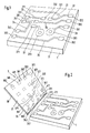
- Fig. 1 one is not yet electronic Components populated circuit board 1, which in the input mentioned sense must be tested with a simple Layout shown in perspective.
- the circuit board 1 has one underside not visible and a top 11 and is then with eight conductor tracks 21, 22, 23, 24, 25, 26, 27, 28 Mistake.
- the conductor track 21 is at one end with one first test point 211 and the conductor track 22 at one End with a second test point 221.
- Another Test point 222 is at the other end of the trace 22; further test points 231, 232; 241, 242; 251, 252; 261, 262 are located at the ends of the conductor tracks 23, 24, 25, 26.
- connection surfaces 273, 283 are also shown, through which through the circuit board electrical connection to any existing, not to seeing conductor tracks on the underside of the circuit board 1 can be manufactured. This is e.g. through by the manufacturer through-metallizations already produced on the circuit board or only by the user of the circuit board using a Component to be soldered releasable.
- test points are created by the user the printed circuit board after delivery electronic Components such as MELF or MiniMELF components appropriate.
- the circuit board 1 is single-ply in Fig. 1 shown, but this is not mandatory.
- test points are during the test process using a Adapter arrangement to a test device, not shown to connect, which is of conventional design, so that its presentation and explanation are omitted here can.
- FIG. 2 is perspective and together with the 1 a first variant of a Adapter arrangement 3 shown.
- a first and a second are on and / or in the film 30 and an nth electrically conductive contact bump 311, 321, 381 arranged. Furthermore, ten further contact bumps 322; 331, 332; 341, 342; 351, 352; 361, 362; 371 available.
- the Reference numerals of the contact bumps are chosen so that their last two digits the last two digits of the Reference numerals of test points 222; 231, 232; 241, 242; 251, 252; 261, 262; 271 are the same.
- the first contact bump 311 On the back of the film 30 is the first contact bump 311 by means of a first conductor track 411 with a first Contact point 511 connected.
- the other conductor lines and no reference numerals assigned to the other contact points are not limited to the other contact points.
- the reference numerals of the conductor tracks are chosen so that their last two digits the last two digits of the Reference numbers for test points 211, 221, 222, 231, 232, 241, 242, 251, 252, 261, 262, 271, 281 and contact bumps 311, 321, 322, 331, 332, 341, 342, 351, 352, 361, 362, 371, 381 are the same.
- the first contact point is 511 with one first contact needle of an input contact field of the Test device, the second contact point 521 with a second Contact pin of the input contact field, the nth Contact point 581 with an nth contact needle and the further contact points of a corresponding one further contact needle of the input contact field electrically to contact.
- the input contact field of the test device has one in lines and Columns regular arrangement of the contact pins mentioned.
- the surface is a mirror image of this arrangement Distribution of the contact points to which the contact points 511, 521, 581 belong.
- the contact bump has a contacting part 3111 and a longitudinal axis 3112. It leads perpendicularly from the Back 32 to front 31 through the film 30 in one Through hole 33, which has a central axis 330.
- Such a contact bump is usually in the bore 33 produces that therein, starting from the Backside 32 existing conductor track 411, galvanic or Electroless copper over the edge at the front 31 bore 33 is grown out.
- This forms a contacting part 3111, the front 31 towered over in one stage and seated in the bore 33 such that the longitudinal axis 3112 coincides with the central axis 330.
- the surface of the contacting part 3111 is one Nickel-gold layer 3113 plated.
- Fig. 3 is also because of the better representation than shown in Fig. 2 that an electrically insulating, resilient intermediate film 34 on the back 32 of the Film 30 is arranged, which e.g. mechanically firm be connected and e.g. made of a suitable foam can exist.
- an electrically insulating, resilient intermediate film 34 on the back 32 of the Film 30 is arranged, which e.g. mechanically firm be connected and e.g. made of a suitable foam can exist.
- the film 30 hugs the pressures mentioned during testing very well to the PCB 1 on, even if they are quite uneven should.
- the first variant of the invention according to FIG. 2 can also be used for double-sided printed circuit boards are used.
- this Case is for the bottom of the two-sided circuit board one corresponding to the adapter arrangement 3 To provide adapter arrangement. This is when testing using one corresponding to the intermediate film 34 Intermediate film to the input contact field of the test device to press.
- the adapter assembly 6 is essentially a single-layer flexible film 60 Insulating material with a front 61 and one Back 62 and with a first part 63 and one with it contiguous second part 64.
- the conductor tracks also extend into the second part 64 the film 60 and end there in associated front side contact points; of these is only that for Fig. 4 Front contact point 652 belonging to contact bump 352 shown.
- the contacting is done by the second part 64 of the Foil 60 is turned by about 180 ° and by that Input contact field on the front 61 of the film 60 in second part 64 pressed, with an intermediate layer an electrically insulating, resilient Intermediate film 74 between the first part 63 and the second part 64 of the rear side 62 of the film 60.
- the intermediate film 74 is only partial in FIG. 5 shown so that it does not cover other parts of the figure.
- the intermediate film 74 exercises its Bump leveling function both at first Part 63 and the circuit board 1 as well as the second Part 64 and the input contact field.
- the second variant of the invention according to FIG. 4 can also can be used together with double-sided printed circuit boards. This is for the back of the two-sided circuit board another one corresponding to the adapter arrangement 6, provide two-part adapter arrangement. This is with Test by turning 180 ° and using one of the Intermediate film 74 corresponding further intermediate film press the input contact field of the test device.
Landscapes
- Engineering & Computer Science (AREA)
- Microelectronics & Electronic Packaging (AREA)
- Computer Hardware Design (AREA)
- General Engineering & Computer Science (AREA)
- Physics & Mathematics (AREA)
- General Physics & Mathematics (AREA)
- Metallurgy (AREA)
- Manufacturing & Machinery (AREA)
- Testing Of Short-Circuits, Discontinuities, Leakage, Or Incorrect Line Connections (AREA)
Priority Applications (1)
| Application Number | Priority Date | Filing Date | Title |
|---|---|---|---|
| EP98116790A EP0902297A3 (fr) | 1997-09-11 | 1998-09-05 | Appareillage adaptateur pour tester des circuits imprimés |
Applications Claiming Priority (3)
| Application Number | Priority Date | Filing Date | Title |
|---|---|---|---|
| EP97810646A EP0902296A1 (fr) | 1997-09-11 | 1997-09-11 | Adaptateurs pour tester des circuits imprimés |
| EP97810646 | 1997-09-11 | ||
| EP98116790A EP0902297A3 (fr) | 1997-09-11 | 1998-09-05 | Appareillage adaptateur pour tester des circuits imprimés |
Publications (2)
| Publication Number | Publication Date |
|---|---|
| EP0902297A2 true EP0902297A2 (fr) | 1999-03-17 |
| EP0902297A3 EP0902297A3 (fr) | 2001-11-28 |
Family
ID=26148060
Family Applications (1)
| Application Number | Title | Priority Date | Filing Date |
|---|---|---|---|
| EP98116790A Withdrawn EP0902297A3 (fr) | 1997-09-11 | 1998-09-05 | Appareillage adaptateur pour tester des circuits imprimés |
Country Status (1)
| Country | Link |
|---|---|
| EP (1) | EP0902297A3 (fr) |
Cited By (1)
| Publication number | Priority date | Publication date | Assignee | Title |
|---|---|---|---|---|
| CN112748322A (zh) * | 2019-10-31 | 2021-05-04 | 南亚科技股份有限公司 | 测试治具及测试组件 |
Family Cites Families (4)
| Publication number | Priority date | Publication date | Assignee | Title |
|---|---|---|---|---|
| US5228189A (en) * | 1988-11-12 | 1993-07-20 | Mania Gmbh & Co. | Adapter arrangement for electrically connecting flat wire carriers |
| US5399982A (en) * | 1989-11-13 | 1995-03-21 | Mania Gmbh & Co. | Printed circuit board testing device with foil adapter |
| JP2733359B2 (ja) * | 1989-12-19 | 1998-03-30 | 日東電工株式会社 | テストヘッド構造 |
| US5252916A (en) * | 1992-01-27 | 1993-10-12 | Everett Charles Technologies, Inc. | Pneumatic test fixture with springless test probes |
-
1998
- 1998-09-05 EP EP98116790A patent/EP0902297A3/fr not_active Withdrawn
Cited By (1)
| Publication number | Priority date | Publication date | Assignee | Title |
|---|---|---|---|---|
| CN112748322A (zh) * | 2019-10-31 | 2021-05-04 | 南亚科技股份有限公司 | 测试治具及测试组件 |
Also Published As
| Publication number | Publication date |
|---|---|
| EP0902297A3 (fr) | 2001-11-28 |
Similar Documents
| Publication | Publication Date | Title |
|---|---|---|
| DE69302400T2 (de) | Testanordnung mit filmadaptor fuer leiterplatten | |
| EP1484950B1 (fr) | Méthode de mise en contact èlectrique | |
| DE3639367C2 (fr) | ||
| DE69200500T2 (de) | Gestufte Mehrlagenverbindungsplatte und Herstellungsmethoden. | |
| DE69011223T2 (de) | Verbinderanordnung mit einem beweglichen Wagen. | |
| DE3634491A1 (de) | Schaltungsplatine und sondenkabelanordnung | |
| EP0838688B1 (fr) | Appareil et procédé de test de circuits imprimés | |
| DE19944980A1 (de) | Ummantelte elektrische Verbindung für eine Anschlußstruktur | |
| DE10015744A1 (de) | Ummantelte elektrische Verbindung für eine Anschlußstruktur | |
| DE2525166A1 (de) | Kontakt-sondenvorrichtung | |
| DE102009049848A1 (de) | Elektrische Verbindungsvorrichtung | |
| DE4129925A1 (de) | Bauelement-testplatte fuer einen halbleiter-bauelement-tester mit einem rekonfigurierbaren koaxialen verbindungsgitter, und verfahren zu dessen gebrauch | |
| EP0106990A1 (fr) | Elément pour faire contact entre des plaquettes à circuit imprimé | |
| DE2453843A1 (de) | Steckverbinder-anordnung | |
| EP0875767B1 (fr) | Appareil et procédé pour tester des circuits imprimés non pourvus de composants | |
| DE69102917T2 (de) | Testgerät für integrierte Schaltkreise. | |
| EP0902297A2 (fr) | Appareillage adaptateur pour tester des circuits imprimés | |
| EP0995235B1 (fr) | Contact pour de minuscules contacts de liaison et procede de production d'un contact | |
| EP0902296A1 (fr) | Adaptateurs pour tester des circuits imprimés | |
| EP1031042B1 (fr) | Dispositif pour verifier des cartes de circuits | |
| CH698875B1 (de) | Verfahren zur Bestückung einer Leiterplatte mit einem Stecker. | |
| DE60201537T2 (de) | Elektrische verbindungsanordnung für elektronische bauteile | |
| DE10324450A1 (de) | Kontaktierungsvorrichtung für elektronische Schaltungseinheiten und Herstellungsverfahren | |
| DE3804425C1 (en) | PCB testing arrangement using several pins - forms contact between test pins and board tracks by compression under vacuum of sheets | |
| DE102024204764B4 (de) | Elektronische Baugruppe |
Legal Events
| Date | Code | Title | Description |
|---|---|---|---|
| PUAI | Public reference made under article 153(3) epc to a published international application that has entered the european phase |
Free format text: ORIGINAL CODE: 0009012 |
|
| AK | Designated contracting states |
Kind code of ref document: A2 Designated state(s): AT BE CH CY DE DK ES FI FR GB GR IE IT LI LU MC NL PT SE |
|
| AX | Request for extension of the european patent |
Free format text: AL;LT;LV;MK;RO;SI |
|
| PUAL | Search report despatched |
Free format text: ORIGINAL CODE: 0009013 |
|
| AK | Designated contracting states |
Kind code of ref document: A3 Designated state(s): AT BE CH CY DE DK ES FI FR GB GR IE IT LI LU MC NL PT SE |
|
| AX | Request for extension of the european patent |
Free format text: AL;LT;LV;MK;RO;SI |
|
| AKX | Designation fees paid | ||
| REG | Reference to a national code |
Ref country code: DE Ref legal event code: 8566 |
|
| 19U | Interruption of proceedings before grant |
Effective date: 20020401 |
|
| 19W | Proceedings resumed before grant after interruption of proceedings |
Effective date: 20100401 |
|
| RAP1 | Party data changed (applicant data changed or rights of an application transferred) |
Owner name: WUERTH ELEKTRONIK SCHOPFHEIM GMBH & CO. KG |
|
| STAA | Information on the status of an ep patent application or granted ep patent |
Free format text: STATUS: THE APPLICATION IS DEEMED TO BE WITHDRAWN |
|
| 18D | Application deemed to be withdrawn |
Effective date: 20020529 |