EP0877503A2 - Prüfmustererzeugungsgerät, Übertragungseinrichtung und Simulator - Google Patents
Prüfmustererzeugungsgerät, Übertragungseinrichtung und Simulator Download PDFInfo
- Publication number
- EP0877503A2 EP0877503A2 EP98108344A EP98108344A EP0877503A2 EP 0877503 A2 EP0877503 A2 EP 0877503A2 EP 98108344 A EP98108344 A EP 98108344A EP 98108344 A EP98108344 A EP 98108344A EP 0877503 A2 EP0877503 A2 EP 0877503A2
- Authority
- EP
- European Patent Office
- Prior art keywords
- test pattern
- synchronous clock
- data
- section
- pattern data
- Prior art date
- Legal status (The legal status is an assumption and is not a legal conclusion. Google has not performed a legal analysis and makes no representation as to the accuracy of the status listed.)
- Granted
Links
Images

Classifications
-
- H—ELECTRICITY
- H04—ELECTRIC COMMUNICATION TECHNIQUE
- H04L—TRANSMISSION OF DIGITAL INFORMATION, e.g. TELEGRAPHIC COMMUNICATION
- H04L1/00—Arrangements for detecting or preventing errors in the information received
- H04L1/24—Testing correct operation
- H04L1/242—Testing correct operation by comparing a transmitted test signal with a locally generated replica
- H04L1/244—Testing correct operation by comparing a transmitted test signal with a locally generated replica test sequence generators
-
- G—PHYSICS
- G06—COMPUTING OR CALCULATING; COUNTING
- G06F—ELECTRIC DIGITAL DATA PROCESSING
- G06F11/00—Error detection; Error correction; Monitoring
- G06F11/22—Detection or location of defective computer hardware by testing during standby operation or during idle time, e.g. start-up testing
- G06F11/26—Functional testing
- G06F11/263—Generation of test inputs, e.g. test vectors, patterns or sequences ; with adaptation of the tested hardware for testability with external testers
Definitions
- the present invention relates to a test pattern generating apparatus for generating a test pattern which evaluate as to whether or not data and synchronous clock are transmitted normally through a bus, a communication device having a test pattern generating apparatus and simulator.
- LAN local area network
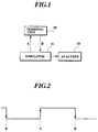
- An evaluation system for making an evaluation of the communication system is, as shown in FIG. 1, for example, composed of a simulator 51, a terminal unit 53 and an analyzer 55.
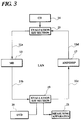
- a communication system between the simulator 51 and terminal unit 53 as shown in FIG. 2, when a synchronous clock in the simulator 51 is changed from negative to positive (timing A), a control command is transmitted from the simulator 51 to the terminal unit 53.
- the simulator 51 receives a response command from the terminal unit 53 and displays the received response command on the analyzer 55.
- the synchronization of the command level can be confirmed.
- test pattern generating apparatus capable of confirming synchronization of source data and bit synchronous clock and make it easy to confirm synchronization of a communication system.
- the present invention has the following arrangement in order to solve the above problem.
- the invention provides a test pattern generating apparatus generating a test pattern evaluating as to whether or not the communication data and a bit synchronous clock are transmitted normally through the bus when a plurality of terminal units for transmitting and receiving communication data are connected to a bus, said apparatus comprising:
- test pattern generating section since the test pattern generating section generates the test pattern data which are predetermined as the test pattern based on the bit synchronous clock and frame synchronous clock and outputs the test pattern data, bit synchronous clock and frame synchronous clock to the bus, disguised data can be confirmed, and further the synchronization of the source data and bit synchronous clock can be confirmed and the synchronization of the communication system can be confirmed easily.
- test pattern data generated by said test pattern generating section may comprise a first test pattern data having a first period in the first half period of the frame synchronous clock and a second test pattern data having a second period which is different from the first period in the latter half period of the frame synchronous clock.
- test patterns are varied per half period of the frame synchronous clock, disguised data can be confirmed easily.
- a communication device confirming and evaluating as to whether or not the communication data and a bit synchronous clock are transmitted normally through the bus when a plurality of terminal units for transmitting and receiving communication data are connected to a bus, said device comprising:
- the received source data and bit synchronous clock are outputted by the input switching section, and in a test mode, the test pattern data generated by the test pattern generating section, bit synchronous clock and frame synchronous clock are outputted by the input switching section.
- test pattern data generated by said test pattern generating section may comprise a first test pattern data having a first period in the first half period of the frame synchronous clock and a second test pattern data having a second period which is different from the first period in the latter half period of the frame synchronous clock.
- a simulator confirming and evaluating as to whether or not the communication data and a bit synchronous clock are transmitted normally through the bus when a plurality of communication devices for transmitting and receiving communication data are connected to a bus, said simulator comprising:
- the received source data and bit synchronous clock are outputted by the input switching section
- the test pattern data generated by the test pattern generating section, bit synchronous clock and frame synchronous clock are outputted by the input switching section.
- the command generating section generates the command including a transmission source address and destination address and adds the command to the source data or test pattern data so as to output them to the bus.
- test pattern data generated by said test pattern generating section may comprise a first test pattern data having a first period in the first half period of the frame synchronous clock and second test pattern data having a second period which is different from the first period in the latter half period of the frame synchronous clock.
- the input switching section may outputs the test pattern data, bit synchronous clock and frame synchronous clock on a display section through the bus.
- test pattern data bit synchronous clock and frame synchronous clock from the input switching section are displayed on the display section, disguised data and synchronization can be confirmed.
- FIG. 1 is a drawing showing an example of connection between the simulator and terminal unit.
- FIG. 2 is a timing chart of a synchronous clock for transmitting and responding a control command between the simulator and terminal unit.
- FIG. 3 is a constitutional drawing showing a communication system including a simulator according to a first embodiment of the present invention.
- FIG. 4 is a constitutional block diagram of an evaluation kit section according to the first embodiment.
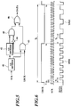
- FIG. 5 is a detailed constitutional drawing of a test pattern generating circuit.
- FIG. 6 is a constitutional drawing of a frame of a synchronous clock and test pattern data.
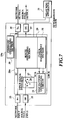
- FIG. 7 is a constitutional block diagram of the evaluation kit section according to a second embodiment of the present invention.
- test pattern generating apparatus communication device
- simulator of the present invention will be described in detail with reference to the accompanying drawings.
- FIG. 3 shows a constitutional drawing of a communication system including the simulator according to a first embodiment.
- a compact disk (CD) 14 outputs digital audio data to an evaluation kit section 15, and the evaluation kit section 15 is connected with buses 11a and 11d.
- the bus 11a is connected with a mini disk (hereinafter, referred to as MD) 13, and the MD 13 is connected with an evaluation kit section 19 through a bus 11b.
- MD mini disk
- the evaluation kit section 19 is connected with an amplifier/display (hereinafter, referred to as AMP/DISP) 17 through a bus 11c, and the AMP/DISP 17 is connected with the evaluation kit section 15 through the bus 11d.
- the evaluation kit section 19 is connected with a digital video disk (DVD) 20 and measuring apparatus 21.
- DVD digital video disk
- the MD 13, evaluation kit section 19, AMP/DISP 17 and evaluation kit section 15 are connected in a closed loop form by the buses 11a through 11d so as to construct a local area network (hereinafter, referred to as LAN).
- LAN local area network
- digital audio data from the CD 14 are transmitted to the evaluation kit section 15, MD 13, evaluation kit section 19 and AMP/DISP 17.
- the digital audio data are composed of a plurality of frames, and the respective frames, in the case of two channels and stereo, are composed of two subframes, i.e., a subframe for L channel and a subframe for R channel. These two subframes are synchronized with a frame synchronous clock LRCK of frame unit so as to be transmitted. Data in the respective subframes are synchronized with a bit synchronous clock SCK of bit unit so as to be transmitted.
- the evaluation kit sections 15 and 19 compose the communication device or simulator, and when an integrated circuit (hereinafter, referred to as IC) is designed, the evaluation kit sections 15 and 19 are evaluation boards for evaluating performance of the IC.
- the evaluation kit sections 15 and 19 monitor and output the synchronous clocks SCK and LRCK and source data to the measuring apparatus 21 such as an analyzer so that synchronization of the bit synchronous clock SCK of bit unit and frame synchronous clock LRCK of frame unit and source data can be confirmed.
- FIG. 4 shows a constitutional block diagram of the evaluation kit sections 15 and 19.
- a network signal receiving section (Rx) 23 receives a network signal from the bus 11b and outputs the network signal to a route switching section 29 in an IC 26.
- a source data receiving section (SR) 25 receives source data such as digital audio data from the DVD 20 and outputs the source data to a switching unit 27 as an input switching section.
- the IC 26 is composed of the route switching section 29 and a clock management section 31 as a clock generating section.
- a common terminal a is connected with one end of a contact piece 28, and the other end of the contact piece 28 is connected selectively with a selection terminal b or selection terminal c.
- the common terminal a is connected with the route switching section 25, and the selection terminal b is connected with an output terminal of the source data receiving section 29, and the selection terminal c is connected with a test pattern generating circuit 33.
- the route switching section 29 switches routes.
- a command generating section 39 generates a command including a transmission source address and destination address adds the command to the source data so as to output the source data to which the command was added to a network signal transmitting section (Tx) 35.
- the clock management section 31 generates a synchronous clock SCK of bit unit as well as a synchronous clock LRCK of frame unit and outputs the synchronous clocks SCK and LRCK to the test pattern generating circuit 33 as a test pattern generating section as well as to the bus 11c through the network signal transmitting section (Tx) 35.
- the test pattern generating circuit 33 generates test pattern data based on the synchronous clocks SCK and LRCK from the clock management section 31, and the test pattern data are previously determined for confirming and evaluating as to whether or not source data and bit synchronous clock are transmitted normally through the buses.
- the test pattern generating circuit 33 and clock management section 31 compose the test pattern generating apparatus, and generate a test pattern for evaluating as to whether or not the source data and bit synchronous clock SCK are transmitted normally through the buses 11a through 11d.
- FIG. 5 shows a detailed constitutional drawing of the test pattern generating circuit 33.
- the test pattern generating circuit 33 is composed of a 1/2 divider 41 for dividing the bit synchronous clock SCK into 1/2, a 1/2 divider 42 for dividing an output of the 1/2 divider 41 into 1/2, an AND circuit 43 for obtaining the logical product of the output of the 1/2 divider 41 and the frame synchronous clock LRCK, a NOT circuit 44 for inverting the frame synchronous clock LRCK, an AND circuit 45 for obtaining the logical product of the output of the NOT circuit 44 and the output of the 1/2 divider 42, and an OR circuit 46 for obtaining the logical OR of the output of the AND circuit 45 and the output of the AND circuit 43.
- the predetermined test pattern data which are generated by the test pattern generating circuit 33, as shown in FIG. 6, are composed of first test pattern data TPD1 having a first period T 3 in the first half period T 1 /2 of the frame synchronous clock LRCK and second test pattern data TPD2 having a second period T 4 which is different from the first period T 3 in the latter half period T 1 /2 of the frame synchronous clock LRCK.
- the switching unit 27 When selecting the selection terminal b, the switching unit 27 outputs source data from the source data receiving section (SR) 25 to the route switching section 29, and when selecting the selection terminal c, it outputs test pattern data from the test pattern generating circuit 33 to the route switching section 29.
- SR source data receiving section
- the network signal transmitting section (Tx) 35 directly outputs the network signal to the bus 11c. Further, the source data from the switching unit 27 or the test pattern data are also outputted to the bus 11c.
- the source data transmitting section (SX) 37 is switched by the route switching section 29 so as to receive the network signal.
- the measuring apparatus 21 is an analyser or the like, and it measures the test pattern data outputted from the source data transmitting section (SX) 37 and the synchronous clocks SCK and LRCK from the IC 26, and displays the measured test pattern data and synchronous clocks SCK and LRCK thereon.
- the arrangement of the evaluation kit section 15 is the same as that of the evaluation kit section 19.
- the following describes an operation of the communication system including the simulator arranged in the above manner.
- evaluation is made as to the case where digital audio data as source data are outputted from the CD 14 to the AMP/DISP 17 and as to the confirmation of the operation of the MD 13 using the evaluation kit sections 15 and 19 and the measuring apparatus 21.
- the evaluation kit sections 15 and 19 and the AMP/DISP 17 should be normal.
- the description is given as to the normal process, namely, output of the digital audio data from the CD 14 to the AMP/DISP 17.
- the digital audio data from the CD 14 and the synchronous clock are inputted to the evaluation kit section 15, and the evaluation kit section 15 transmits the digital audio data and synchronous clocks to the MD 13 through the network signal receiving section (Rx) 23, IC 26, network signal transmitting section (Tx) 35, bus 11a, etc.
- the digital audio data and synchronous clock received by the MD 13 are transmitted to the evaluation kit section 19 through the bus 11b, and the digital audio data in the evaluation kit section 19 are transmitted to the AMP/DISP 17 through the network signal receiving section (Rx) 23, IC 26, network signal transmitting section (Tx) 35 and bus 11c.
- the digital audio data are amplified in the AMP/DISP 17.
- the contact piece 28 selects the selection terminal c in the switching unit 27 of the evaluation kit section 15. Then, the test pattern generating circuit 33 generates predetermined test pattern data which are previously determined based on the synchronous clocks SCK and LRCK from the clock management section 31.
- LRCK 1/2 period of LRCK
- the 1/2 divider 41 divides the bit synchronous clock SCK into 1/2, and when the AND circuit 43 obtains the logical product of the output of the 1/2 divider 41 and the frame synchronous clock LRCK, its output is the same as the output of the 1/2 divider 41, and the output of the 1/2 divider 41 is inputted into the OR circuit 46.
- the 1/2 divider 42 divides the output of the 1/2 divider 41 into 1/2, and the NOT circuit 44 inverts the frame synchronous clock LRCK. Since the AND circuit 45 obtains the logical product of the output of the NOT circuit 44 and the output of the 1/2 divider 42, its output becomes "0". For this reason, the output of the OR circuit 46 becomes the output of the 1/2 divider 41 in the first 1/2 period of LRCK. In the similar manner, LRCK is "0" in the latter 1/2 period of LRCK, so the output of the OR circuit 46 becomes the output of the 1/2 divider 42.
- test pattern data are transmitted to the network signal transmitting section (Tx) 35 through the switching unit 27 and route switching section 29.
- the synchronous clocks SCK and LRCK from the clock management section 31 are transmitted to the network signal transmitting section (Tx) 35 through the route switching section 29.
- the test pattern data and synchronous clocks SCK and LRCK are transmitted to the evaluation kit section 19 through the bus 11a, MD 13 and bus 11b.
- test pattern data and synchronous clocks SCK and LRCK are received by the network signal receiving section (Rx) 23 and are inputted to the source data transmitting section (SX) 37 through the route switching section 29.
- the test pattern data and synchronous clocks SCK and LRCK from the source data transmitting section (SX) 37 are transmitted to the measuring apparatus 21 so as to be displayed thereon.
- FIG. 6 shows on example of the synchronous clocks LRCK and SCK and test pattern data (DATA) displayed on the measuring apparatus 21.
- the period of the frame synchronous clock LRCK is T 1
- the period of the bit synchronous clock SCK is T 2 .
- the bit synchronous clock SCK is displayed in 32 bits/frame. Namely, the bit synchronous clocks SCK of 32 bits exists in one period T 1 of the frame synchronous clock LRCK.
- the test pattern is first test pattern data TPD1 having a first period T 3
- the test pattern is second test pattern data TPD2 having a period T 4 twice as much as the first period T 3 . Since test pattern is changed per half period of the frame synchronous clock LRCK, L and R can be identified.
- the test pattern displayed on the measuring apparatus 21 becomes the second test pattern data TPD2 in the first half period T 1 /2 of the frame synchronous clock LRCK
- the test pattern becomes the first test pattern data TPD1 in the latter half period T 1 /2 of the frame synchronous clock LRCK
- L and R of the test pattern to be displayed are contrary to L and R of the predetermined test pattern
- occurrence of disguised data can be confirmed.
- the connection and operation of the MD 13 can be evaluated as abnormal.
- the cause of this abnormality for example, it is considered that routes of L and R of the MD 13 are reversed.
- test pattern generating circuit 33 since the test pattern generating circuit 33 generates test pattern data which are similar to the predetermined synchronous clock based on the synchronous clock and transmits the generated test pattern data instead of source data at the time of the confirmation of synchronization, disguised data can be confirmed.
- the evaluation kit sections 15 and 19 monitor and output the synchronous clocks SCK and LRCK and source data to the measuring apparatus 21 such as an analyzer, the synchronization of the synchronous clocks SCK and LRCK and digital audio data as source data can be confirmed easily.
- FIG. 7 shows a constitutional block diagram of the evaluation kit section according to the second embodiment of the present invention.
- the arrangement of the communication system is substantially same as that of the first embodiment shown in FIG. 3, but the evaluation kit section 19 shown in FIG. 3 corresponds to an evaluation kit section 19a in FIG. 7, and the evaluation kit section 15 shown in FIG. 3 corresponds to an evaluation kit section 15a in FIG. 7.
- the arrangement of the evaluation kit section 15a is the same as that of the evaluation kit section 19a.
- the evaluation kit section 19a shown in FIG. 7 is characterized by including the test pattern generating circuit 33 and switching unit 27 in an IC 26a.
- the evaluation kit section 19a is composed of the network signal receiving section (Rx) 23, source data receiving section (SR) 25, network signal transmitting section (Tx) 35, source data transmitting section (SX) 37, and the IC 26a which is connected to the above sections.
- the IC 26a is composed of the switching unit 27, test pattern generating circuit 33, route switching section 29 and clock management section 31.
- digital audio data from the CD 14 are transmitted to the evaluation kit section 19a through the evaluation kit section 15a and MD 13, and the digital audio data in the evaluation kit section 19a are transmitted to the AMP/DISP 17 through the network signal receiving section (Rx) 23, IC 26, network signal transmitting section (Tx) 35 and bus 11c.
- the digital audio data are outputted to the AMP/DISP 17.
- the contact piece 28 selects the selection terminal c in the switching unit 27 in the IC 26a of the evaluation kit section 15a, and the test pattern generating circuit 33 in the IC 26a generates predetermined test pattern data show in FIG. 4 based on synchronous clocks SCK and LRCK from the clock management section 31.
- test pattern data and synchronous clocks SCK and LRCK are transmitted to the MD 13 through the IC 26a, network signal transmitting section (Tx) 35, bus 11a, etc. and are sent to the evaluation kit section 19a through the MD 13.
- test pattern data and synchronous clocks SCK and LRCK are received by the network signal receiving section (Rx) 23 and are inputted to the source data transmitting section (SX) 37 through the route switching section 29.
- the test pattern data and synchronous clocks SCK and LRCK from the source data transmitting section (SX) 37 are transmitted to the measuring apparatus 21 so as to be displayed on the measuring apparatus 21.
- the test pattern generating circuit 33 when in the IC 26a the test pattern generating circuit 33 generates test pattern data and the switching unit 27 selects to the selection terminal c in the IC 26a, similarly to the first embodiment, disguised data can be confirmed, and further the synchronization of the test pattern data and synchronous clocks can be confirmed, so the synchronization of the communication system is confirmed easily.
- Embodiments 1 and 2 refers to the digital audio data communication, but for example, in packet communication where packet data are transmitted and received in DVD 20, by adding header information including a transmission source address and destination address to the test pattern waveform, the present invention is applicable.
- test pattern generating section since the test pattern generating section generates test pattern data, which are predetermined as a test pattern, based on bit synchronous clock and frame synchronous clock so as to output the test pattern data and bit synchronous clock and frame synchronous clock to the bus, disguised data can be confirmed, and further the synchronization of source data and bit synchronous clock can be confirmed, and the synchronization of the communication system can be confirmed easily.
- test patterns are varied per half period of the frame synchronous clock, disguised data can be confirmed easily.
- received communication data and bit synchronous clock can be outputted by the input switching section
- test pattern data generated by the test pattern generating section, bit synchronous clock and frame synchronous clock can be outputted by the input switching section.
- the command generating section can generate a command including a transmission source address and destination address and can output the command to the bus.
- test pattern data bit synchronous clock and frame synchronous clock from the input switching section are displayed on the display section, disguised data and synchronization can be confirmed.
Landscapes
- Engineering & Computer Science (AREA)
- Computer Networks & Wireless Communication (AREA)
- Signal Processing (AREA)
- Maintenance And Management Of Digital Transmission (AREA)
- Small-Scale Networks (AREA)
- Synchronisation In Digital Transmission Systems (AREA)
- Test And Diagnosis Of Digital Computers (AREA)
Applications Claiming Priority (3)
| Application Number | Priority Date | Filing Date | Title |
|---|---|---|---|
| JP11831297 | 1997-05-08 | ||
| JP11831297A JP3628477B2 (ja) | 1997-05-08 | 1997-05-08 | テストパターン生成装置、通信装置及びシミュレータ |
| JP118312/97 | 1997-05-08 |
Publications (3)
| Publication Number | Publication Date |
|---|---|
| EP0877503A2 true EP0877503A2 (de) | 1998-11-11 |
| EP0877503A3 EP0877503A3 (de) | 2000-12-06 |
| EP0877503B1 EP0877503B1 (de) | 2005-08-31 |
Family
ID=14733571
Family Applications (1)
| Application Number | Title | Priority Date | Filing Date |
|---|---|---|---|
| EP98108344A Expired - Lifetime EP0877503B1 (de) | 1997-05-08 | 1998-05-07 | Prüfmustererzeugungsgerät, Übertragungseinrichtung und Simulator |
Country Status (4)
| Country | Link |
|---|---|
| US (1) | US6088824A (de) |
| EP (1) | EP0877503B1 (de) |
| JP (1) | JP3628477B2 (de) |
| DE (1) | DE69831367T2 (de) |
Cited By (1)
| Publication number | Priority date | Publication date | Assignee | Title |
|---|---|---|---|---|
| US6973603B2 (en) * | 2002-06-28 | 2005-12-06 | Intel Corporation | Method and apparatus for optimizing timing for a multi-drop bus |
Family Cites Families (6)
| Publication number | Priority date | Publication date | Assignee | Title |
|---|---|---|---|---|
| US4247941A (en) * | 1979-06-28 | 1981-01-27 | Honeywell Information Systems Inc. | Simulator for bit and byte synchronized data network |
| FR2643203B1 (fr) * | 1989-02-10 | 1991-05-31 | Delisle Dominique | Emulateurs de terminaison numerique de reseau et systemes de controle et mesure de bus |
| US5231598A (en) * | 1991-09-30 | 1993-07-27 | National Semiconductor Corporation | Direct digital synthesis measurement signal skew tester |
| US5383195A (en) * | 1992-10-19 | 1995-01-17 | Motorola, Inc. | BIST circuit with halt signal |
| US5309428A (en) * | 1993-01-11 | 1994-05-03 | John Fluke Mfg. Co., Inc. | Token ring local area network testing apparatus for phase jitter testing |
| WO1997011381A1 (fr) * | 1995-09-22 | 1997-03-27 | Advantest Corporation | Controleur de memoire |
-
1997
- 1997-05-08 JP JP11831297A patent/JP3628477B2/ja not_active Expired - Fee Related
-
1998
- 1998-05-05 US US09/071,891 patent/US6088824A/en not_active Expired - Fee Related
- 1998-05-07 EP EP98108344A patent/EP0877503B1/de not_active Expired - Lifetime
- 1998-05-07 DE DE69831367T patent/DE69831367T2/de not_active Expired - Fee Related
Cited By (3)
| Publication number | Priority date | Publication date | Assignee | Title |
|---|---|---|---|---|
| US6973603B2 (en) * | 2002-06-28 | 2005-12-06 | Intel Corporation | Method and apparatus for optimizing timing for a multi-drop bus |
| US7117401B2 (en) | 2002-06-28 | 2006-10-03 | Intel Corporation | Method and apparatus for optimizing timing for a multi-drop bus |
| CN100378704C (zh) * | 2002-06-28 | 2008-04-02 | 英特尔公司 | 用于优化多点总线的时序的方法和装置 |
Also Published As
| Publication number | Publication date |
|---|---|
| JPH10308760A (ja) | 1998-11-17 |
| EP0877503B1 (de) | 2005-08-31 |
| DE69831367D1 (de) | 2005-10-06 |
| DE69831367T2 (de) | 2006-06-22 |
| US6088824A (en) | 2000-07-11 |
| JP3628477B2 (ja) | 2005-03-09 |
| EP0877503A3 (de) | 2000-12-06 |
Similar Documents
| Publication | Publication Date | Title |
|---|---|---|
| KR100435629B1 (ko) | 데이터 전송 장치, 표시 장치, 데이터 송신 장치, 데이터수신 장치, 데이터 전송 방법 | |
| KR100847505B1 (ko) | 전원 공급 시스템 및 직렬 통신 장치 | |
| JPS6125229A (ja) | Ic装置 | |
| US6088824A (en) | Test pattern generating apparatus, communication device and simulator | |
| US5268932A (en) | Interface circuit between a plurality of transmission lines and high bit rate data terminal equipment | |
| JP3326137B2 (ja) | 直列通信インターフェース回路 | |
| JPH057230A (ja) | 同期データ・インターフエース回路 | |
| JP3565326B2 (ja) | 半導体装置およびそれを搭載して成る回路モジュール | |
| JPH02127688A (ja) | 陰極線管表示装置制御方式 | |
| JPH05134007A (ja) | 半導体集積論理回路 | |
| JPS63164555A (ja) | 伝送ラインモニタ装置 | |
| US6097738A (en) | Multi-speed retainer | |
| JP2718746B2 (ja) | 端末インタフェースの受信データ制御回路 | |
| JP4182096B2 (ja) | 擬似基地局装置 | |
| KR100397336B1 (ko) | 전송시스템의 멀티프레임펄스 안정화장치 | |
| JP2815041B2 (ja) | Lsi内部状態確認回路 | |
| JP2002208916A (ja) | 自動位相調整回路及びデータ通信システム | |
| JP3005548B1 (ja) | 無線電話機の誤り率測定システム及び誤り率測定方法 | |
| JPH01123562A (ja) | 制御チャンネル置換制御方式 | |
| JP2003125026A (ja) | 通信回線テスト方法 | |
| JPH1168720A (ja) | 伝送路の二重通信方式 | |
| JP2003174632A (ja) | 相互同期型映像伝送装置 | |
| JP2869284B2 (ja) | シグナリング信号誤り保護回路 | |
| KR100210780B1 (ko) | 프로세서와 디바이스간의 타임 슬롯 스위치의 데이터 정합회로 | |
| KR20010063618A (ko) | 전자파를 감소시키기 위한 데이터 신호 전송 회로 |
Legal Events
| Date | Code | Title | Description |
|---|---|---|---|
| PUAI | Public reference made under article 153(3) epc to a published international application that has entered the european phase |
Free format text: ORIGINAL CODE: 0009012 |
|
| 17P | Request for examination filed |
Effective date: 19980507 |
|
| AK | Designated contracting states |
Kind code of ref document: A2 Designated state(s): DE FR GB |
|
| AX | Request for extension of the european patent |
Free format text: AL;LT;LV;MK;RO;SI |
|
| PUAL | Search report despatched |
Free format text: ORIGINAL CODE: 0009013 |
|
| AK | Designated contracting states |
Kind code of ref document: A3 Designated state(s): AT BE CH CY DE DK ES FI FR GB GR IE IT LI LU MC NL PT SE |
|
| AX | Request for extension of the european patent |
Free format text: AL;LT;LV;MK;RO;SI |
|
| AKX | Designation fees paid |
Free format text: DE FR GB |
|
| 17Q | First examination report despatched |
Effective date: 20040719 |
|
| GRAP | Despatch of communication of intention to grant a patent |
Free format text: ORIGINAL CODE: EPIDOSNIGR1 |
|
| GRAS | Grant fee paid |
Free format text: ORIGINAL CODE: EPIDOSNIGR3 |
|
| GRAA | (expected) grant |
Free format text: ORIGINAL CODE: 0009210 |
|
| AK | Designated contracting states |
Kind code of ref document: B1 Designated state(s): DE FR GB |
|
| REG | Reference to a national code |
Ref country code: GB Ref legal event code: FG4D |
|
| REF | Corresponds to: |
Ref document number: 69831367 Country of ref document: DE Date of ref document: 20051006 Kind code of ref document: P |
|
| PGFP | Annual fee paid to national office [announced via postgrant information from national office to epo] |
Ref country code: GB Payment date: 20060503 Year of fee payment: 9 |
|
| ET | Fr: translation filed | ||
| PGFP | Annual fee paid to national office [announced via postgrant information from national office to epo] |
Ref country code: DE Payment date: 20060508 Year of fee payment: 9 |
|
| PGFP | Annual fee paid to national office [announced via postgrant information from national office to epo] |
Ref country code: FR Payment date: 20060515 Year of fee payment: 9 |
|
| PLBE | No opposition filed within time limit |
Free format text: ORIGINAL CODE: 0009261 |
|
| STAA | Information on the status of an ep patent application or granted ep patent |
Free format text: STATUS: NO OPPOSITION FILED WITHIN TIME LIMIT |
|
| 26N | No opposition filed |
Effective date: 20060601 |
|
| GBPC | Gb: european patent ceased through non-payment of renewal fee |
Effective date: 20070507 |
|
| REG | Reference to a national code |
Ref country code: FR Ref legal event code: ST Effective date: 20080131 |
|
| PG25 | Lapsed in a contracting state [announced via postgrant information from national office to epo] |
Ref country code: DE Free format text: LAPSE BECAUSE OF NON-PAYMENT OF DUE FEES Effective date: 20071201 |
|
| PG25 | Lapsed in a contracting state [announced via postgrant information from national office to epo] |
Ref country code: GB Free format text: LAPSE BECAUSE OF NON-PAYMENT OF DUE FEES Effective date: 20070507 |
|
| PG25 | Lapsed in a contracting state [announced via postgrant information from national office to epo] |
Ref country code: FR Free format text: LAPSE BECAUSE OF NON-PAYMENT OF DUE FEES Effective date: 20070531 |