EP0871843B1 - Mounting member and method for clamping a flat thin conductive workpiece - Google Patents
Mounting member and method for clamping a flat thin conductive workpiece Download PDFInfo
- Publication number
- EP0871843B1 EP0871843B1 EP95936873A EP95936873A EP0871843B1 EP 0871843 B1 EP0871843 B1 EP 0871843B1 EP 95936873 A EP95936873 A EP 95936873A EP 95936873 A EP95936873 A EP 95936873A EP 0871843 B1 EP0871843 B1 EP 0871843B1
- Authority
- EP
- European Patent Office
- Prior art keywords
- electrodes
- gas
- wafer
- workpiece
- platen
- Prior art date
- Legal status (The legal status is an assumption and is not a legal conclusion. Google has not performed a legal analysis and makes no representation as to the accuracy of the status listed.)
- Expired - Lifetime
Links
Images

Classifications
-
- H10P72/0434—
-
- H10P72/0432—
-
- H10P72/72—
-
- Y—GENERAL TAGGING OF NEW TECHNOLOGICAL DEVELOPMENTS; GENERAL TAGGING OF CROSS-SECTIONAL TECHNOLOGIES SPANNING OVER SEVERAL SECTIONS OF THE IPC; TECHNICAL SUBJECTS COVERED BY FORMER USPC CROSS-REFERENCE ART COLLECTIONS [XRACs] AND DIGESTS
- Y10—TECHNICAL SUBJECTS COVERED BY FORMER USPC
- Y10T—TECHNICAL SUBJECTS COVERED BY FORMER US CLASSIFICATION
- Y10T279/00—Chucks or sockets
- Y10T279/23—Chucks or sockets with magnetic or electrostatic means
Definitions
- the present invention relates to a mounting member for clamping a flat thin workpiece and it also relates to a method of electrostatic clamping.
- US-A-5179498 discloses an electrostatic chuck device with a strong chucking force.
- the chuck device is said to be capable of easily loading/unloading an object to be chucked and providing sure grounding for a semiconductor wafer.
- Three-phase AC voltages of one Hz or less with different phases are applied, and contact pins with pointed tips are provided.
- US-A-5 184 398 reveals the features of the preamble of claim 1.
- electrostatic clamping for resistive workpieces
- the electrostatic clamp includes a plurality of long, thin electrode regions which are activated in a sequence different from their spatial ordering to provide a non-motoring by dynamic pattern of clamping forces.
- a semiconductor wafer 2 is clamped with a ring clamp 30 against a cooled flat support member 23.
- An O-ring 20 set in the surface of the support 23 directly opposite the ring clamp provides a seal to confine gas which is introduced under pressure through an orifice 22 into the space between the wafer and the support member.
- This technology has been used in ion implantation, but has disadvantages which include applying stress to the wafer, and generation of particles on the front side of the wafer, loss of usable area of semiconductor wafer material due to masking by the clamp ring, sputtering of contaminants from the clamp ring onto the wafer, and a less than optimal cooling effectiveness, since the cooling which can be obtained is reduced due to bowing of the wafer under the influences of localized clamping on the front and uniform gas pressure on the rear surfaces.
- a platen 36 is gently domed so that the action of clamping the wafer 2 at its periphery with ring 42 against the platen 36 causes the wafer to gently bend over the platen and to bear against the platen with an approximately uniform degree of contact prior to introduction of gas under pressure through channel 37.
- the domed shape of the platen prevents the separation of wafer and platen, at moderate gas pressures. As discussed in the cited patents, too great a separation is known to reduce the level of obtainable thermal transfer, so this construction attains better cooling characteristics.
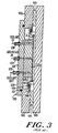
- FIG. 3 shows a variation of the prior art approach shown in FIG. 1, with the stage, clamping, and cooling mechanisms integrated into a wafer holding assembly.
- the wafer 2 rests vertically against a heat sink member 119 that is actively cooled by a flow of fluid through inlet and outlet tubes 128, 129.
- the front face of the member 119 has a central flat recessed floor 125, and a plurality of small clip assemblies 103, which each are moved by a machine actuated mechanism 104, hold the wafer 2 down against a peripheral lip of the heat sink, so that the wafer is close to, but not touching the face 125.
- a central gas inlet feeds argon at 100-1000 microns pressure into the space between the wafer and heat sink to raise the pressure and increase the rate of heat transfer.
- the gas When used for heating a wafer the gas may be heated.
- the gas pressure When used for cooling, the gas pressure is ten or more times greater than the residual gas pressure in the chamber, and a certain amount of the heat transfer gas leaks out past edges of the wafer to maintain the normal ten micron chamber pressure of a sputtering chamber.
- the heat sink is mounted on a backing plate 120 that seals against the vacuum chamber wall 102 via an 0-ring seal 121, and when not in its operative position, the opening in wall 102 is covered by a pressure plate 105 and seal ring 101.
- Both the gas introduction passage 126 and the fluid heat exchange passages 128, 129 for the heat exchange plate pass through the backing plate 120. While the edge clips 103 reduce somewhat the wasted wafer area given over to the clamp ring in the construction of Figure 1, the problems inherent in that construction remain.
- An embodiment departs from these prior art approaches in providing gas under pressure as a thermal transfer medium into a space of random variations formed between two flat and mutually contacting surfaces while the workpiece is urged with a force distributed over its entire surface against a platen over a broad contact area.
- Gas is introduced along a peripheral line contour to provide substantially uniform thermal conduction.
- the workpiece is a thin flat wafer, and the workpieces are heated or cooled by mounting each workpiece to a very flat platen with substantially uniform pressure, and by introducing the gas between the wafer and the platen.
- the platen is made as flat as practical, preferably better than +/- 0.0127mm (0.0005"), with the exception of holes and grooves for the transfer medium as described further below, and is polished smooth.
- both the platen and the workpiece are made sufficiently flat to come into uniform contact or substantially uniformly contacting proximity, and are made smooth with a microscopic roughness preferably not exceeding 0.813 ⁇ m (32 micro inches).
- the gas occupies the microscopic valley spaces in the surfaces of the platen and the workpiece.
- a small rate of leakage of gas from the edges of the platen is matched by a constant flow of gas introduced by way of a groove or ring of holes in the platen surface, running along a contour fairly close to the edge of the wafer, into the region between the workpiece and the platen.
- the area of gas introduction forms an isobaric boundary around the center of the wafer space, which otherwise has no gas outlet. This assures that, despite the irregular shape and very narrow dimension of the space occupied by the transfer medium, the gas remains distributed uniformly under the workpiece, in a wafer-to-platen gap that is smaller than the mean free path length of the gas. Conductive heat transfer is therefore maximized.
- the pressure applied between the workpiece and the platen is low and is substantially uniform over the full surface of the platen. Clamping forces are applied by electrostatic clamping for moderately conductive workpieces such as silicon wafers.
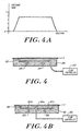
- FIG. 4 a flat thin workpiece 2 is placed in high vacuum upon a flat platen 201, through which a liquid such as water is passed in channels 204.
- the liquid can be heated, cooled or maintained at a reference temperature as required for the process and substances involved.
- a gas is introduced at a flow controlled by flow controller 205 at a rate of approximately 0.25 sccm into a conduit or channel that feeds via a ring or circular groove 203 into the interface between the workpiece and the platen.
- This groove or ring of holes 203 is referred to below as the gas introduction ring.
- the pressure of the cooling gas is controlled, in accordance with this embodiment the mass flow is controlled. This important difference produces effects in several ways described more fully below which, in conjunction with the lack of a peripheral seal and the use of highly flat surfaces, assure that both the pressure and the nominal thermal transfer gap spacing are kept quite low, while obtaining high rate of heat transfer.
- the photoresist When a wafer is partially covered with a photoresist mask undergoing ion implantation, the photoresist alone can be a source of several standard cubic centimeters per minute (sccm) of hydrogen gas liberated by the action of the ion beam on the organic photoresist.
- sccm standard cubic centimeters per minute
- the leakage by a wafer cooling system of a small fraction of one sccm of gas, possibly hydrogen may not significantly affect the implantation process, particularly if the reduction in temperature of the wafer achieved by such cooling has a compensating negative effect upon the volume of hydrogen being liberated by the resist.
- the gas cooling system may safely introduce a certain amount of gas, especially if, as described above, the amount of cooling gas is less than the amount by which the temperature change reduces outgassing. Based on this realization, applicant has determined a structure for a heat exchange platen to operate with such a defined flow of gas leakage.
- the surface of a semiconductor wafer has a roughness within conventionally attained finishing standards of, for example, 0.385 ⁇ m (twelve micro inches) r.m.s., and defects in flatness of up to several 2.54 ⁇ m (ten thousandths of an inch) are allowed to occur.
- Applicant advantageously utilizes these surface variations to maintain firm contact between the workpiece and the platen with additional conductive heat transfer effected by a gas at low gas pressure and flow rates matched to the irregular interstitial heat transfer space defined by the foregoing surface finish features as discussed further below.
- FIG. 4a shows a graph of gas pressure within the wafer/platen interstitial space as a function of position from one side of the wafer to the other.
- the pressure of gas reaches a steady state shortly after the gas flow commences. In practice, this pump-up interval is found to be one second or less.
- the pressure profile beneath the wafer in the absence of the mechanical edge clamping and elastomer sealing shown would be high at the center relative to the edges. This would introduce non-uniform heat transfer, and the rate of gas leakage would also have to be much higher to maintain suitable pressure at the edge.
- the introduction of the gas in a contour close to the edge of the platen allows the pressure to come to static equilibrium over an interior region covering the greater part of the space between the wafer and the workpiece, as shown by the pressure profile in FIG. 4a, without requiring such high pressure to achieve effective heat conduction. Applicant achieves this without use of clamp rings or seals, and is therefore able to avoid pressure-distortion of the wafer.
- the platen may be provided with a gas introduction hole 203a at its center, as in Figure 1, but with this hole linked by one or more grooves 203b, 203c which extend to an outer groove 203 occupying a peripheral contour close to the edge of the platen.
- the linking groove or grooves 203b, 203c may be located below the face of the platen as illustrated, or may consist of narrow channels in the face itself. In either case, they serve as pressure shunts to uniformize the pressure distribution under the workpiece, again producing a substantially constant pressure distribution as shown in Figure 4A and allowing operation at a minimal heat transfer fluid pressure simultaneously with minimal distortion of the thin workpiece, and effective thermal regulation is achieved without excessive leakage of fluid into the process chamber.
- C 2 ⁇ rg 2 c/3l
- the rate of cooling is proportional to the gas flow, proportional to the distance from the gas introduction ring 3 to the platen edge, and inversely proportional to the mean square gap.
- the mean square gap is determined by the surface finish and flatness of the workpiece and of the platen. Interestingly, in these equations the choice of gas only enters through the effect of ⁇ .
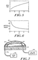
- the mean free path also depends upon the atomic/molecular number A of the gas selected, as shown in FIG. 6. Both pressure and mean free path may also be affected by chemical properties of the gas not discussed further here. The importance of the mean free path is that if it is less than the gap such that a significant number of gas-gas collisions occur between the workpiece and the platen, then the cooling rate is considerably reduced. A discussion of the relationship between the gap and mean free path in their effect in heat transfer rate may be found in the two patents noted above.
- the gas heat transfer medium introduced at the periphery of the wafer need not enter via a full circular port. Instead, a plurality of discrete inlet ports 203a, 203b, ... may be distributed along a closed contour in a peripheral region of the platen. In that case, diffusive flow of the gas operates to smooth the overall distribution profile. In each case, the result is a substantially constant and stationary gas profile in the central region, and a small but balanced flow of gas with a decreasing pressure profile across the thin peripheral band region outside of the gas introduction contour.
- leakage of gas into the high vacuum chamber is further reduced to a small fraction of the rate at which the gas is supplied by the flow controller 205, by providing a gas scavenger assembly along the diffusion path between the inlet orifice and the vacuum chamber.
- platen 201 is situated in a high vacuum chamber (not shown) and a workpiece (not shown for clarity) is placed upon the flat surface 209 of the platen.
- Gas is introduced through the first annular groove 203, and a second annular groove 207 (or ring of holes) located radially outward from groove 203 surrounds the inlet.
- the second groove is located approximately one and a half millimeters inwardly from the outer edge of the platen 201.
- the second groove 207 connects via a passage to a mechanical vacuum pump 206 that provides differential pumping, i.e. pumping to a vacuum level higher than the manifold pressure of inlet 203, and close to or even higher than the vacuum level in the surrounding chamber.
- a mechanical vacuum pump 206 that provides differential pumping, i.e. pumping to a vacuum level higher than the manifold pressure of inlet 203, and close to or even higher than the vacuum level in the surrounding chamber.
- the cooling or heating gas leaks radially outward in the interstitial space, it enters this groove, and the greater part of it is removed from the system by pump 206 without traveling further outward or leaking into the high vacuum chamber.
- the cooling gas does not compromise the high vacuum environment in which the wafer is processed.
- One or more large conduits 207a lead from the scavenging groove 207 to the pump 206, making the conductance of the path from groove 207 to pump 206 substantially greater than the conductance from groove 207 into the vacuum chamber, thus favoring scavenging of gas along the out-diffusion route.
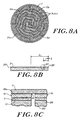
- FIGS. 8a, 8b and 8c The preferred embodiment of the invention 250 is illustrated in FIGS. 8a, 8b and 8c.
- the platen of this system includes an electrostatic clamp to apply pressure which holds the wafer workpiece to the platen.
- This method works well for conductive workpieces. The technique is similar to that described by J. Ballou, K. Carson, W. Frutiger, J. Greco and R. Kaim in Proceedings of the Ion Implantation Technology Conference IIT '94, Catania, Italy .
- the workpiece-contacting (front) surface of the platen 250 includes a flat lapped and polished sheet of a dielectric material, 52, composed, for example, of aluminum oxide, with a thickness preferably between about (0.15)-(0.2) millimeters, and which forms a plurality of operative charging regions defined by a metallized electrode pattern deposited on its back surface.
- the metallized back pattern provides a set of plural electrodes 51 of approximately equal area, preferably differing by under one-quarter of one percent.
- electrodes 51a, 51b, 51c, 51d of spiral shape each approximately ten millimeters in width and less than one-quarter millimeter thick, and each electrically separated from the others by a small in-plane gap of up to several millimeters or more, define a set of closely spaced charging regions that collectively cover the front surface of the platen.
- the electrodes are long and thin, and each covers a path along a dispersed region of the circular wafer that is interdigitated with the other electrode regions.
- the spiral form is not itself critical. but merely represents one option for forming such a regular electrode pattern, and deviations from a regular plane spiral shape may also be made to accommodate electrode connections or when convenient for other reasons.
- the regular electrode pattern is preferably formed of regions that are not large isolated blocks, and do not correspond to nodal regions of lower order wafer resonances, so that the necessary fluctuations in force caused by the clamp drive signals cannot induce large mechanical vibrations.
- the flat conductive workpiece 2 of the polished dielectric layer 52 is omitted for clarity, and electrodes 51 are shown visible through the dielectric layer 52, which is typically transparent or translucent.
- FIG. 8b shows a vertical section through the platen 250, with a wafer 2 of radius R lying flat on the platen surface so that it covers the gas introduction inlet 203 positioned at radial distance of (R-1), from the center and also covers the gas scavenging groove 207, lying at a distance ⁇ inward from the wafer edge.
- the view of FIG. 8c is an enlargement of part of the cross section to more clearly illustrate the layered construction. Workpiece 2 is shown.
- Its plate-contacting surface 2a has micro-roughness as described above, which forms the roughened ceiling of a crack-like opening 2b allowing the passage of gas, while the alumina dielectric layer 52 has a generally smoother and flatter surface 52a, which may, for example, be optically polished and which acts as a floor of the gas-filled space. Electrodes 51 are sandwiched between the alumina dielectric layer 52 and another dielectric layer 53. which may be a hard inorganic material like layer 52 or may be an organic polymer and which also effects a bond to the underlying body of platen 250.
- the entire top surface of this assembly is preferably lapped to a flatness of (0.0125) millimetres or better, and polished to a finish which is preferably better than about 0.2 ⁇ m (eight micro inches) r.m.s.
- the dielectric layer 52 is bounded by the groove 207, and the upper face of the outer wall of this groove is also lapped and polished, forming part of the same flat plane as the top of layer 52.
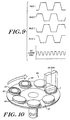
- FIG. 9 indicates a set of signal waveforms and preferred phase relationships for these clamp operating signals.
- Each signal is a periodically repeating trapezoidal wave shape that ramps up and down between an upper potential u and a lower potential l , and each is identical to the others except for phase, the first and fourth being of opposite phase, as are the second and third signals, while the first and second signals are shifted by a quarter period with respect to each other.
- the wafer 2 lying on top of layer 52 serves as a common electrode for charging all four of the dielectric regions over the spiral electrode arms 5 1a-51d, and the applied voltages generate an electric field of about 5 MV/m or more between the electrodes and the surface of the wafer.
- the width of the electrodes is small, preferably under ten millimeters. This reduces the amplitude of any vibration, and raises the resonant frequencies of any vibrational modes which might be excited in the wafer or platen, ensuring that the vibration induced by the spatially- and time-varying clamping forces is far removed from any mechanical resonance of the platen or workpiece.
- each electrode shaped in a spiral pattern is used, and a four-phase a.c. trapezoidal waveform is applied.
- the electrodes are arranged in pairs that receive actuating signals that are exactly out of phase, with one signal ramping up while the other signal of a pair is ramping down.
- another region is clamped with a fixed voltage at maximum magnitude so the dips occur in isolated regions.
- the invention also contemplates clamping with larger even numbers of electrodes and phases. By providing an even number of phases, applicant ensures that the potential of the wafer is unaffected by the application of the electrostatic clamping signal waveforms.
- phase sequence is applied to non-sequential electrodes, for example 1-2-4-3 or 1-3-4-2; this removes any "motoring" component from the forces imparted to the wafer and avoids generating traveling waves which would have a tendency to move the wafer in a single direction.
- the current flowing to the electrodes of the electrostatic clamp will be reduced when the wafer is not in intimate contact with the dielectric, since the introduction of an additional air gap between the wafer and the back electrodes greatly decreases capacitance.
- Applicant exploits this latter feature by monitoring clamp current for example, with threshold detectors. The threshold crossing may trigger an alarm. That is, automatic measurement of this current immediately indicates the presence of a particle and/or incorrect placement of the workpiece.
- a set of platens 401 similar to those shown in FIG. 4 or FIG. 7 are mounted to a spinning disk or drum 55 in a surface region that is inclined with respect to the plane of rotation such that centripetal force urges each wafer against the face of the platen as the wafers are rotated past a treatment station.
- a set of radial arms as shown in Robinson et al., U.S. Patent No. 4,733,091 may be used to impart such a centrifugal clamping mechanism.
- a component of centripetal force is developed, which acts to press the workpieces onto the platens while holding them in an orientation for processing.
- the invention disclosed herein although mainly described as applied to circular semiconductor wafers, is readily adapted to other shapes and other materials, e.g., to square or rectangular flat substrates such as sensors, flat panel displays, and other shapes or articles requiring vacuum treatment.
- the peripheral gas introduction channel or ring, and the scavenging or differential pumping ring, if one is used, will in general each lie on a non-circular contour.
- the principal of operation is in other respects similar, and for non-circular substrates the advantages of distributed clamp force and uniform heat transfer characteristics may be expected to offer even more significant improvements over presently available workholders and thermal control systems.
Landscapes
- Container, Conveyance, Adherence, Positioning, Of Wafer (AREA)
Applications Claiming Priority (3)
| Application Number | Priority Date | Filing Date | Title |
|---|---|---|---|
| US32376494A | 1994-10-17 | 1994-10-17 | |
| US323764 | 1994-10-17 | ||
| PCT/US1995/013158 WO1996013058A2 (en) | 1994-10-17 | 1995-10-17 | Apparatus and method for temperature control of workpieces in vacuum |
Publications (3)
| Publication Number | Publication Date |
|---|---|
| EP0871843A4 EP0871843A4 (OSRAM) | 1998-10-21 |
| EP0871843A2 EP0871843A2 (en) | 1998-10-21 |
| EP0871843B1 true EP0871843B1 (en) | 2003-05-14 |
Family
ID=23260617
Family Applications (1)
| Application Number | Title | Priority Date | Filing Date |
|---|---|---|---|
| EP95936873A Expired - Lifetime EP0871843B1 (en) | 1994-10-17 | 1995-10-17 | Mounting member and method for clamping a flat thin conductive workpiece |
Country Status (5)
| Country | Link |
|---|---|
| US (1) | US5822172A (OSRAM) |
| EP (1) | EP0871843B1 (OSRAM) |
| JP (1) | JP4079992B2 (OSRAM) |
| DE (1) | DE69530801T2 (OSRAM) |
| WO (1) | WO1996013058A2 (OSRAM) |
Families Citing this family (47)
| Publication number | Priority date | Publication date | Assignee | Title |
|---|---|---|---|---|
| US5679404A (en) * | 1995-06-07 | 1997-10-21 | Saint-Gobain/Norton Industrial Ceramics Corporation | Method for depositing a substance with temperature control |
| KR100290264B1 (ko) * | 1997-01-22 | 2001-09-22 | 호소이 쇼지로 | 정전처크장치 및 그 제조방법 |
| JPH10240356A (ja) * | 1997-02-21 | 1998-09-11 | Anelva Corp | 基板処理装置の基板温度制御法と基板温度制御性判定法 |
| US6207005B1 (en) | 1997-07-29 | 2001-03-27 | Silicon Genesis Corporation | Cluster tool apparatus using plasma immersion ion implantation |
| US6274459B1 (en) | 1998-02-17 | 2001-08-14 | Silicon Genesis Corporation | Method for non mass selected ion implant profile control |
| US6113735A (en) * | 1998-03-02 | 2000-09-05 | Silicon Genesis Corporation | Distributed system and code for control and automation of plasma immersion ion implanter |
| JP2000021964A (ja) | 1998-07-06 | 2000-01-21 | Ngk Insulators Ltd | 静電チャックのパーティクル発生低減方法および半導体製造装置 |
| FR2785737B1 (fr) * | 1998-11-10 | 2001-01-05 | Semco Engineering Sa | Dispositif de maintien electrostatique |
| US6303411B1 (en) | 1999-05-03 | 2001-10-16 | Vortek Industries Ltd. | Spatially resolved temperature measurement and irradiance control |
| WO2001004945A1 (en) * | 1999-07-08 | 2001-01-18 | Lam Research Corporation | Electrostatic chuck and its manufacturing method |
| EP1224687A2 (en) * | 1999-10-01 | 2002-07-24 | Varian Semiconductor Equipment Associates Inc. | Surface structure and method of making, and electrostatic wafer clamp incorporating surface structure |
| US6362946B1 (en) * | 1999-11-02 | 2002-03-26 | Varian Semiconductor Equipment Associates, Inc. | Electrostatic wafer clamp having electrostatic seal for retaining gas |
| US6538873B1 (en) | 1999-11-02 | 2003-03-25 | Varian Semiconductor Equipment Associates, Inc. | Active electrostatic seal and electrostatic vacuum pump |
| US6583858B2 (en) * | 2000-03-16 | 2003-06-24 | Asml Netherlands B.V. | Substrate holder for lithographic apparatus |
| US6736952B2 (en) * | 2001-02-12 | 2004-05-18 | Speedfam-Ipec Corporation | Method and apparatus for electrochemical planarization of a workpiece |
| TWI272689B (en) * | 2001-02-16 | 2007-02-01 | Tokyo Electron Ltd | Method and apparatus for transferring heat from a substrate to a chuck |
| US6998353B2 (en) * | 2001-11-05 | 2006-02-14 | Ibis Technology Corporation | Active wafer cooling during damage engineering implant to enhance buried oxide formation in SIMOX wafers |
| JP2005515425A (ja) | 2001-12-26 | 2005-05-26 | ボルテック インダストリーズ リミテッド | 温度測定および熱処理方法およびシステム |
| US6734117B2 (en) * | 2002-03-12 | 2004-05-11 | Nikon Corporation | Periodic clamping method and apparatus to reduce thermal stress in a wafer |
| US20040066601A1 (en) * | 2002-10-04 | 2004-04-08 | Varian Semiconductor Equipment Associates, Inc. | Electrode configuration for retaining cooling gas on electrostatic wafer clamp |
| KR101163682B1 (ko) | 2002-12-20 | 2012-07-09 | 맷슨 테크날러지 캐나다 인코퍼레이티드 | 피가공물 지지 장치 |
| US7283346B2 (en) * | 2002-12-26 | 2007-10-16 | Mitsubishi Heavy Industries, Ltd. | Electrostatic chuck and its manufacturing method |
| US6934595B1 (en) * | 2003-02-26 | 2005-08-23 | National Semiconductor Corp. | Method and system for reducing semiconductor wafer breakage |
| US7357115B2 (en) * | 2003-03-31 | 2008-04-15 | Lam Research Corporation | Wafer clamping apparatus and method for operating the same |
| US7151658B2 (en) * | 2003-04-22 | 2006-12-19 | Axcelis Technologies, Inc. | High-performance electrostatic clamp comprising a resistive layer, micro-grooves, and dielectric layer |
| JP5630935B2 (ja) | 2003-12-19 | 2014-11-26 | マトソン テクノロジー、インコーポレイテッド | 工作物の熱誘起運動を抑制する機器及び装置 |
| US7352554B2 (en) * | 2004-06-30 | 2008-04-01 | Axcelis Technologies, Inc. | Method for fabricating a Johnsen-Rahbek electrostatic wafer clamp |
| US20060060145A1 (en) * | 2004-09-17 | 2006-03-23 | Van Den Berg Jannes R | Susceptor with surface roughness for high temperature substrate processing |
| US7126091B1 (en) | 2005-03-23 | 2006-10-24 | Eclipse Energy Systems, Inc. | Workpiece holder for vacuum processing |
| JP5967859B2 (ja) | 2006-11-15 | 2016-08-10 | マトソン テクノロジー、インコーポレイテッド | 熱処理中の被加工物を支持するシステムおよび方法 |
| TWI459851B (zh) * | 2007-09-10 | 2014-11-01 | 日本碍子股份有限公司 | heating equipment |
| EP2095946A1 (en) | 2008-02-27 | 2009-09-02 | Nederlandse Organisatie voor toegepast- natuurwetenschappelijk onderzoek TNO | A system for patterning flexible foils |
| US9558980B2 (en) | 2008-04-30 | 2017-01-31 | Axcelis Technologies, Inc. | Vapor compression refrigeration chuck for ion implanters |
| US9036326B2 (en) * | 2008-04-30 | 2015-05-19 | Axcelis Technologies, Inc. | Gas bearing electrostatic chuck |
| US9070590B2 (en) | 2008-05-16 | 2015-06-30 | Mattson Technology, Inc. | Workpiece breakage prevention method and apparatus |
| JP2010123810A (ja) * | 2008-11-20 | 2010-06-03 | Ulvac Japan Ltd | 基板保持装置及び基板温度制御方法 |
| US8004817B2 (en) * | 2009-06-18 | 2011-08-23 | Varian Semiconductor Equipment Associates, Inc. | Method of platen fabrication to allow electrode pattern and gas cooling optimization |
| FR2974251B1 (fr) | 2011-04-18 | 2013-11-01 | Ecole Polytech | Dispositif pour la gestion thermique d'un élément optique et procédé de gestion thermique associe. |
| JP5550602B2 (ja) * | 2011-04-28 | 2014-07-16 | パナソニック株式会社 | 静電チャックおよびこれを備えるドライエッチング装置 |
| KR20140053323A (ko) * | 2011-08-19 | 2014-05-07 | 울박, 인크 | 진공 처리 장치 및 진공 처리 방법 |
| JP5505667B2 (ja) * | 2011-09-30 | 2014-05-28 | Toto株式会社 | 交流駆動静電チャック |
| US10032601B2 (en) * | 2014-02-21 | 2018-07-24 | Varian Semiconductor Equipment Associates, Inc. | Platen support structure |
| KR101877452B1 (ko) * | 2016-05-19 | 2018-08-09 | 한국기계연구원 | 도전 물질의 패터닝 장치 및 방법 |
| JP7020951B2 (ja) * | 2018-02-09 | 2022-02-16 | 東京エレクトロン株式会社 | プラズマ処理システムおよびプラズマ処理方法 |
| KR20210089375A (ko) * | 2020-01-08 | 2021-07-16 | 주식회사 미코세라믹스 | 정전척 |
| JP7183223B2 (ja) * | 2020-08-28 | 2022-12-05 | 株式会社Screenホールディングス | 基板処理装置および基板処理方法 |
| US11417557B2 (en) | 2020-12-15 | 2022-08-16 | Entegris, Inc. | Spiraling polyphase electrodes for electrostatic chuck |
Citations (2)
| Publication number | Priority date | Publication date | Assignee | Title |
|---|---|---|---|---|
| US4457359A (en) * | 1982-05-25 | 1984-07-03 | Varian Associates, Inc. | Apparatus for gas-assisted, solid-to-solid thermal transfer with a semiconductor wafer |
| US5179498A (en) * | 1990-05-17 | 1993-01-12 | Tokyo Electron Limited | Electrostatic chuck device |
Family Cites Families (15)
| Publication number | Priority date | Publication date | Assignee | Title |
|---|---|---|---|---|
| US4261762A (en) | 1979-09-14 | 1981-04-14 | Eaton Corporation | Method for conducting heat to or from an article being treated under vacuum |
| US4603466A (en) * | 1984-02-17 | 1986-08-05 | Gca Corporation | Wafer chuck |
| WO1988009054A1 (en) * | 1987-05-06 | 1988-11-17 | Labtam Limited | Electrostatic chuck using ac field excitation |
| US4949783A (en) * | 1988-05-18 | 1990-08-21 | Veeco Instruments, Inc. | Substrate transport and cooling apparatus and method for same |
| JPH03227554A (ja) * | 1990-02-01 | 1991-10-08 | Tokyo Electron Ltd | 静電チャック |
| US5452177A (en) * | 1990-06-08 | 1995-09-19 | Varian Associates, Inc. | Electrostatic wafer clamp |
| EP0460955A1 (en) * | 1990-06-08 | 1991-12-11 | Varian Associates, Inc. | Clamping a workpiece utilizing polyphase clamping voltage |
| US5184398A (en) * | 1991-08-30 | 1993-02-09 | Texas Instruments Incorporated | In-situ real-time sheet resistance measurement method |
| US5315473A (en) * | 1992-01-21 | 1994-05-24 | Applied Materials, Inc. | Isolated electrostatic chuck and excitation method |
| US5460684A (en) * | 1992-12-04 | 1995-10-24 | Tokyo Electron Limited | Stage having electrostatic chuck and plasma processing apparatus using same |
| US5444597A (en) * | 1993-01-15 | 1995-08-22 | Blake; Julian G. | Wafer release method and apparatus |
| US5436790A (en) * | 1993-01-15 | 1995-07-25 | Eaton Corporation | Wafer sensing and clamping monitor |
| US5345999A (en) * | 1993-03-17 | 1994-09-13 | Applied Materials, Inc. | Method and apparatus for cooling semiconductor wafers |
| EP0635870A1 (en) * | 1993-07-20 | 1995-01-25 | Applied Materials, Inc. | An electrostatic chuck having a grooved surface |
| US5474614A (en) * | 1994-06-10 | 1995-12-12 | Texas Instruments Incorporated | Method and apparatus for releasing a semiconductor wafer from an electrostatic clamp |
-
1995
- 1995-10-17 DE DE69530801T patent/DE69530801T2/de not_active Expired - Fee Related
- 1995-10-17 JP JP51399296A patent/JP4079992B2/ja not_active Expired - Lifetime
- 1995-10-17 EP EP95936873A patent/EP0871843B1/en not_active Expired - Lifetime
- 1995-10-17 WO PCT/US1995/013158 patent/WO1996013058A2/en not_active Ceased
-
1997
- 1997-01-07 US US08/779,899 patent/US5822172A/en not_active Expired - Lifetime
Patent Citations (2)
| Publication number | Priority date | Publication date | Assignee | Title |
|---|---|---|---|---|
| US4457359A (en) * | 1982-05-25 | 1984-07-03 | Varian Associates, Inc. | Apparatus for gas-assisted, solid-to-solid thermal transfer with a semiconductor wafer |
| US5179498A (en) * | 1990-05-17 | 1993-01-12 | Tokyo Electron Limited | Electrostatic chuck device |
Also Published As
| Publication number | Publication date |
|---|---|
| EP0871843A4 (OSRAM) | 1998-10-21 |
| WO1996013058A3 (en) | 1996-06-27 |
| DE69530801T2 (de) | 2004-03-11 |
| DE69530801D1 (de) | 2003-06-18 |
| US5822172A (en) | 1998-10-13 |
| JPH11504760A (ja) | 1999-04-27 |
| EP0871843A2 (en) | 1998-10-21 |
| JP4079992B2 (ja) | 2008-04-23 |
| WO1996013058A2 (en) | 1996-05-02 |
Similar Documents
| Publication | Publication Date | Title |
|---|---|---|
| EP0871843B1 (en) | Mounting member and method for clamping a flat thin conductive workpiece | |
| US5880923A (en) | Method and apparatus for improved retention of a semiconductor wafer within a semiconductor wafer processing system | |
| US5903428A (en) | Hybrid Johnsen-Rahbek electrostatic chuck having highly resistive mesas separating the chuck from a wafer supported thereupon and method of fabricating same | |
| US6095083A (en) | Vacuum processing chamber having multi-mode access | |
| EP1166323B1 (en) | Method and apparatus for compensating non-uniform wafer processing in plasma processing | |
| US5675471A (en) | Characterization, modeling, and design of an electrostatic chuck with improved wafer temperature uniformity | |
| US5846375A (en) | Area specific temperature control for electrode plates and chucks used in semiconductor processing equipment | |
| US6538873B1 (en) | Active electrostatic seal and electrostatic vacuum pump | |
| JP3225850B2 (ja) | 静電吸着電極およびその製作方法 | |
| US20020005252A1 (en) | Plasma etching apparatus and plasma etching method | |
| KR20110020269A (ko) | 정전 척 | |
| US5511608A (en) | Clampless vacuum heat transfer station | |
| KR19980024679A (ko) | 정전 척과 그것을 이용한 시료처리방법 및 장치 | |
| KR20010042592A (ko) | 웨이퍼 미립자 오염 정도가 낮은 정전 웨이퍼 클램프 | |
| JP2001502116A (ja) | 高密度プラズマの化学気相堆積用の可変高温チャック | |
| JP2011519486A (ja) | ガスベアリング静電チャック | |
| JPH10256360A (ja) | 静電チャックの改良型表面形状構造及びその製造方法 | |
| JP6469985B2 (ja) | プラズマ処理装置 | |
| IL123843A (en) | Method and device for electrostatic coupling for dielectric workers in vacuum processes | |
| JP3949186B2 (ja) | 基板載置台、プラズマ処理装置及び半導体装置の製造方法 | |
| JPH07321188A (ja) | 静電チャック表面を誘電性物質の層で被覆する装置 | |
| JP4780410B2 (ja) | 抵抗層、マイクロ溝及び誘電体層を含む高機能静電クランプ | |
| KR100188455B1 (ko) | 드라이 에칭방법 | |
| TW200807551A (en) | Apparatus and method for processing plasma | |
| US5789324A (en) | Uniform gas flow arrangements |
Legal Events
| Date | Code | Title | Description |
|---|---|---|---|
| PUAI | Public reference made under article 153(3) epc to a published international application that has entered the european phase |
Free format text: ORIGINAL CODE: 0009012 |
|
| 17P | Request for examination filed |
Effective date: 19970428 |
|
| A4 | Supplementary search report drawn up and despatched |
Effective date: 19980223 |
|
| AK | Designated contracting states |
Kind code of ref document: A4 Designated state(s): DE GB NL Kind code of ref document: A2 Designated state(s): DE GB NL |
|
| RAP1 | Party data changed (applicant data changed or rights of an application transferred) |
Owner name: VARIAN SEMICONDUCTOR EQUIPMENT ASSOCIATES INC. |
|
| 17Q | First examination report despatched |
Effective date: 20000717 |
|
| GRAH | Despatch of communication of intention to grant a patent |
Free format text: ORIGINAL CODE: EPIDOS IGRA |
|
| RTI1 | Title (correction) |
Free format text: APPARATUS AND METHOD FOR CLAMPING A FLAT THIN CONDUCTIVE WORKPIECE |
|
| RTI1 | Title (correction) |
Free format text: MOUNTING MEMBER AND METHOD FOR CLAMPING A FLAT THIN CONDUCTIVE WORKPIECE |
|
| GRAH | Despatch of communication of intention to grant a patent |
Free format text: ORIGINAL CODE: EPIDOS IGRA |
|
| GRAA | (expected) grant |
Free format text: ORIGINAL CODE: 0009210 |
|
| AK | Designated contracting states |
Designated state(s): DE GB NL |
|
| REG | Reference to a national code |
Ref country code: GB Ref legal event code: FG4D |
|
| REF | Corresponds to: |
Ref document number: 69530801 Country of ref document: DE Date of ref document: 20030618 Kind code of ref document: P |
|
| PLBE | No opposition filed within time limit |
Free format text: ORIGINAL CODE: 0009261 |
|
| STAA | Information on the status of an ep patent application or granted ep patent |
Free format text: STATUS: NO OPPOSITION FILED WITHIN TIME LIMIT |
|
| 26N | No opposition filed |
Effective date: 20040217 |
|
| PGFP | Annual fee paid to national office [announced via postgrant information from national office to epo] |
Ref country code: NL Payment date: 20040929 Year of fee payment: 10 |
|
| PGFP | Annual fee paid to national office [announced via postgrant information from national office to epo] |
Ref country code: GB Payment date: 20051013 Year of fee payment: 11 |
|
| PGFP | Annual fee paid to national office [announced via postgrant information from national office to epo] |
Ref country code: DE Payment date: 20051130 Year of fee payment: 11 |
|
| PG25 | Lapsed in a contracting state [announced via postgrant information from national office to epo] |
Ref country code: NL Free format text: LAPSE BECAUSE OF NON-PAYMENT OF DUE FEES Effective date: 20060501 |
|
| NLV4 | Nl: lapsed or anulled due to non-payment of the annual fee |
Effective date: 20060501 |
|
| PG25 | Lapsed in a contracting state [announced via postgrant information from national office to epo] |
Ref country code: DE Free format text: LAPSE BECAUSE OF NON-PAYMENT OF DUE FEES Effective date: 20070501 |
|
| GBPC | Gb: european patent ceased through non-payment of renewal fee |
Effective date: 20061017 |
|
| PG25 | Lapsed in a contracting state [announced via postgrant information from national office to epo] |
Ref country code: GB Free format text: LAPSE BECAUSE OF NON-PAYMENT OF DUE FEES Effective date: 20061017 |