EP0860873B1 - Klebefolie zum Einsetzen von Wafern und Herstellungsverfahren von elektronischen Bauteilen - Google Patents
Klebefolie zum Einsetzen von Wafern und Herstellungsverfahren von elektronischen Bauteilen Download PDFInfo
- Publication number
- EP0860873B1 EP0860873B1 EP98301322A EP98301322A EP0860873B1 EP 0860873 B1 EP0860873 B1 EP 0860873B1 EP 98301322 A EP98301322 A EP 98301322A EP 98301322 A EP98301322 A EP 98301322A EP 0860873 B1 EP0860873 B1 EP 0860873B1
- Authority
- EP
- European Patent Office
- Prior art keywords
- antiexpansibility
- adhesive sheet
- wafer setting
- film
- adhesive
- Prior art date
- Legal status (The legal status is an assumption and is not a legal conclusion. Google has not performed a legal analysis and makes no representation as to the accuracy of the status listed.)
- Expired - Lifetime
Links
Images
Classifications
-
- C—CHEMISTRY; METALLURGY
- C09—DYES; PAINTS; POLISHES; NATURAL RESINS; ADHESIVES; COMPOSITIONS NOT OTHERWISE PROVIDED FOR; APPLICATIONS OF MATERIALS NOT OTHERWISE PROVIDED FOR
- C09J—ADHESIVES; NON-MECHANICAL ASPECTS OF ADHESIVE PROCESSES IN GENERAL; ADHESIVE PROCESSES NOT PROVIDED FOR ELSEWHERE; USE OF MATERIALS AS ADHESIVES
- C09J7/00—Adhesives in the form of films or foils
- C09J7/20—Adhesives in the form of films or foils characterised by their carriers
- C09J7/22—Plastics; Metallised plastics
-
- H—ELECTRICITY
- H10—SEMICONDUCTOR DEVICES; ELECTRIC SOLID-STATE DEVICES NOT OTHERWISE PROVIDED FOR
- H10W—GENERIC PACKAGES, INTERCONNECTIONS, CONNECTORS OR OTHER CONSTRUCTIONAL DETAILS OF DEVICES COVERED BY CLASS H10
- H10W72/00—Interconnections or connectors in packages
- H10W72/30—Die-attach connectors
-
- H—ELECTRICITY
- H10—SEMICONDUCTOR DEVICES; ELECTRIC SOLID-STATE DEVICES NOT OTHERWISE PROVIDED FOR
- H10W—GENERIC PACKAGES, INTERCONNECTIONS, CONNECTORS OR OTHER CONSTRUCTIONAL DETAILS OF DEVICES COVERED BY CLASS H10
- H10W72/00—Interconnections or connectors in packages
- H10W72/071—Connecting or disconnecting
- H10W72/073—Connecting or disconnecting of die-attach connectors
-
- H—ELECTRICITY
- H10—SEMICONDUCTOR DEVICES; ELECTRIC SOLID-STATE DEVICES NOT OTHERWISE PROVIDED FOR
- H10W—GENERIC PACKAGES, INTERCONNECTIONS, CONNECTORS OR OTHER CONSTRUCTIONAL DETAILS OF DEVICES COVERED BY CLASS H10
- H10W72/00—Interconnections or connectors in packages
- H10W72/071—Connecting or disconnecting
- H10W72/073—Connecting or disconnecting of die-attach connectors
- H10W72/07331—Connecting techniques
- H10W72/07337—Connecting techniques using a polymer adhesive, e.g. an adhesive based on silicone or epoxy
-
- H—ELECTRICITY
- H10—SEMICONDUCTOR DEVICES; ELECTRIC SOLID-STATE DEVICES NOT OTHERWISE PROVIDED FOR
- H10W—GENERIC PACKAGES, INTERCONNECTIONS, CONNECTORS OR OTHER CONSTRUCTIONAL DETAILS OF DEVICES COVERED BY CLASS H10
- H10W72/00—Interconnections or connectors in packages
- H10W72/30—Die-attach connectors
- H10W72/351—Materials of die-attach connectors
- H10W72/353—Materials of die-attach connectors not comprising solid metals or solid metalloids, e.g. ceramics
- H10W72/354—Materials of die-attach connectors not comprising solid metals or solid metalloids, e.g. ceramics comprising polymers
-
- Y—GENERAL TAGGING OF NEW TECHNOLOGICAL DEVELOPMENTS; GENERAL TAGGING OF CROSS-SECTIONAL TECHNOLOGIES SPANNING OVER SEVERAL SECTIONS OF THE IPC; TECHNICAL SUBJECTS COVERED BY FORMER USPC CROSS-REFERENCE ART COLLECTIONS [XRACs] AND DIGESTS
- Y10—TECHNICAL SUBJECTS COVERED BY FORMER USPC
- Y10S—TECHNICAL SUBJECTS COVERED BY FORMER USPC CROSS-REFERENCE ART COLLECTIONS [XRACs] AND DIGESTS
- Y10S156/00—Adhesive bonding and miscellaneous chemical manufacture
- Y10S156/918—Delaminating processes adapted for specified product, e.g. delaminating medical specimen slide
- Y10S156/93—Semiconductive product delaminating, e.g. delaminating emiconductive wafer from underlayer
-
- Y—GENERAL TAGGING OF NEW TECHNOLOGICAL DEVELOPMENTS; GENERAL TAGGING OF CROSS-SECTIONAL TECHNOLOGIES SPANNING OVER SEVERAL SECTIONS OF THE IPC; TECHNICAL SUBJECTS COVERED BY FORMER USPC CROSS-REFERENCE ART COLLECTIONS [XRACs] AND DIGESTS
- Y10—TECHNICAL SUBJECTS COVERED BY FORMER USPC
- Y10S—TECHNICAL SUBJECTS COVERED BY FORMER USPC CROSS-REFERENCE ART COLLECTIONS [XRACs] AND DIGESTS
- Y10S438/00—Semiconductor device manufacturing: process
- Y10S438/976—Temporary protective layer
-
- Y—GENERAL TAGGING OF NEW TECHNOLOGICAL DEVELOPMENTS; GENERAL TAGGING OF CROSS-SECTIONAL TECHNOLOGIES SPANNING OVER SEVERAL SECTIONS OF THE IPC; TECHNICAL SUBJECTS COVERED BY FORMER USPC CROSS-REFERENCE ART COLLECTIONS [XRACs] AND DIGESTS
- Y10—TECHNICAL SUBJECTS COVERED BY FORMER USPC
- Y10T—TECHNICAL SUBJECTS COVERED BY FORMER US CLASSIFICATION
- Y10T156/00—Adhesive bonding and miscellaneous chemical manufacture
- Y10T156/11—Methods of delaminating, per se; i.e., separating at bonding face
-
- Y—GENERAL TAGGING OF NEW TECHNOLOGICAL DEVELOPMENTS; GENERAL TAGGING OF CROSS-SECTIONAL TECHNOLOGIES SPANNING OVER SEVERAL SECTIONS OF THE IPC; TECHNICAL SUBJECTS COVERED BY FORMER USPC CROSS-REFERENCE ART COLLECTIONS [XRACs] AND DIGESTS
- Y10—TECHNICAL SUBJECTS COVERED BY FORMER USPC
- Y10T—TECHNICAL SUBJECTS COVERED BY FORMER US CLASSIFICATION
- Y10T428/00—Stock material or miscellaneous articles
- Y10T428/21—Circular sheet or circular blank
- Y10T428/218—Aperture containing
-
- Y—GENERAL TAGGING OF NEW TECHNOLOGICAL DEVELOPMENTS; GENERAL TAGGING OF CROSS-SECTIONAL TECHNOLOGIES SPANNING OVER SEVERAL SECTIONS OF THE IPC; TECHNICAL SUBJECTS COVERED BY FORMER USPC CROSS-REFERENCE ART COLLECTIONS [XRACs] AND DIGESTS
- Y10—TECHNICAL SUBJECTS COVERED BY FORMER USPC
- Y10T—TECHNICAL SUBJECTS COVERED BY FORMER US CLASSIFICATION
- Y10T428/00—Stock material or miscellaneous articles
- Y10T428/24—Structurally defined web or sheet [e.g., overall dimension, etc.]
- Y10T428/24479—Structurally defined web or sheet [e.g., overall dimension, etc.] including variation in thickness
- Y10T428/24488—Differential nonuniformity at margin
-
- Y—GENERAL TAGGING OF NEW TECHNOLOGICAL DEVELOPMENTS; GENERAL TAGGING OF CROSS-SECTIONAL TECHNOLOGIES SPANNING OVER SEVERAL SECTIONS OF THE IPC; TECHNICAL SUBJECTS COVERED BY FORMER USPC CROSS-REFERENCE ART COLLECTIONS [XRACs] AND DIGESTS
- Y10—TECHNICAL SUBJECTS COVERED BY FORMER USPC
- Y10T—TECHNICAL SUBJECTS COVERED BY FORMER US CLASSIFICATION
- Y10T428/00—Stock material or miscellaneous articles
- Y10T428/24—Structurally defined web or sheet [e.g., overall dimension, etc.]
- Y10T428/24942—Structurally defined web or sheet [e.g., overall dimension, etc.] including components having same physical characteristic in differing degree
-
- Y—GENERAL TAGGING OF NEW TECHNOLOGICAL DEVELOPMENTS; GENERAL TAGGING OF CROSS-SECTIONAL TECHNOLOGIES SPANNING OVER SEVERAL SECTIONS OF THE IPC; TECHNICAL SUBJECTS COVERED BY FORMER USPC CROSS-REFERENCE ART COLLECTIONS [XRACs] AND DIGESTS
- Y10—TECHNICAL SUBJECTS COVERED BY FORMER USPC
- Y10T—TECHNICAL SUBJECTS COVERED BY FORMER US CLASSIFICATION
- Y10T428/00—Stock material or miscellaneous articles
- Y10T428/24—Structurally defined web or sheet [e.g., overall dimension, etc.]
- Y10T428/24942—Structurally defined web or sheet [e.g., overall dimension, etc.] including components having same physical characteristic in differing degree
- Y10T428/2495—Thickness [relative or absolute]
-
- Y—GENERAL TAGGING OF NEW TECHNOLOGICAL DEVELOPMENTS; GENERAL TAGGING OF CROSS-SECTIONAL TECHNOLOGIES SPANNING OVER SEVERAL SECTIONS OF THE IPC; TECHNICAL SUBJECTS COVERED BY FORMER USPC CROSS-REFERENCE ART COLLECTIONS [XRACs] AND DIGESTS
- Y10—TECHNICAL SUBJECTS COVERED BY FORMER USPC
- Y10T—TECHNICAL SUBJECTS COVERED BY FORMER US CLASSIFICATION
- Y10T428/00—Stock material or miscellaneous articles
- Y10T428/28—Web or sheet containing structurally defined element or component and having an adhesive outermost layer
- Y10T428/2848—Three or more layers
Definitions
- the present invention has been made with a view toward resolving the above problem of the prior art.
- the process for producing an electronic component according to the present invention comprises a step of expanding an adhesive sheet, wherein the above adhesive sheet for wafer setting according to the present invention is used as the adhesive sheet.
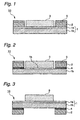
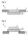
- the antiexpansibility increasing film 2 may be disposed on the marginal part of the adhesive layer 1a of the adhesive sheet 1, as shown in Fig. 1.
- the antiexpansibility increasing film 2 may be laminated either directly or through the medium of an adhesive layer 4 onto the marginal part of the surface of the expansible film 1b.
- the antiexpansibility increasing film 2 may be laminated either directly or through the medium of an adhesive layer 4 onto another surface (back of the expansible film 1b) of the expansible film 1b opposite to the adhesive layer.
- the expansible film 1b is not particularly limited, it is preferred that the expansible film have high water and heat resistances and be composed of a synthetic resin.
- suitable expansible films 1b include films of low density polyethylene (LDPE), linear low density polyethylene (LLDPE), ethylene/propylene copolymer, polypropylene, polybutene, polybutadiene, polymethylpentene, ethylene/vinyl acetate copolymer, ethylene/ (meth(meth)acrylic acid copolymer, ethylene/methyl(meth)acrylate copolymer, ethylene/ethyl (meth)acrylate copolymer, polyvinyl chloride, vinyl chloride/vinyl acetate copolymer, ethylene/vinyl chloride/vinyl acetate copolymer, polyurethanes, polyamides, ionomers, styrene/butadiene rubber and products of hydrogenation or other modification of styrene/butadiene rubber.
- LDPE low density polyethylene
- LLDPE linear low density polyethylene
- ethylene/propylene copolymer polypropylene
- the antiexpansibility increasing film 2 and the expansible film 1b can be laminated onto each other by, for example, heat sealing.
Landscapes
- Chemical & Material Sciences (AREA)
- Organic Chemistry (AREA)
- Dicing (AREA)
- Adhesive Tapes (AREA)
- Adhesives Or Adhesive Processes (AREA)
- Laminated Bodies (AREA)
Claims (4)
- Klebelage zum Waferaufbau, umfassend:dadurch gekennzeichnet, dass:ein Waferaufbauteil umfassend eine expandierbare Folie und eine Klebeschicht zum Waferaufbau; undeinen Randteil außerhalb des Waferaufbauteils und zumindest innerhalb des Teils der Klebelage, auf den ein ringförmiger Rahmen appliziert werden kann,welche größer ist als die des Waferaufbauteils.der Randteil eine Antiexpansionsfähigkeit besitzt, ausgedrückt durch die folgende Formel:
- Klebelage zum Waferaufbau nach Anspruch 1, worin der Randteil eine Antiexpansionsfähigkeit besitzt, welche mindestens das 1,3-fache derjenigen des Waferaufbauteils beträgt.
- Klebelage zum Waferaufbau nach Anspruch 1, worin eine die Antiexpansionsfähigkeit steigernde Folie auf den Randteil der Klebelage laminiert ist.
- Verfahren zur Herstellung eines elektronischen Bauteils, umfassend einen Schritt des Expandierens einer Klebeblage,
worin die Klebelage die Klebelage zum Waferaufbau nach einem der Ansprüche 1 bis 3 ist.
Applications Claiming Priority (3)
| Application Number | Priority Date | Filing Date | Title |
|---|---|---|---|
| JP3919697 | 1997-02-24 | ||
| JP39196/97 | 1997-02-24 | ||
| JP9039196A JPH10242084A (ja) | 1997-02-24 | 1997-02-24 | ウェハ貼着用粘着シートおよび電子部品の製造方法 |
Publications (2)
| Publication Number | Publication Date |
|---|---|
| EP0860873A1 EP0860873A1 (de) | 1998-08-26 |
| EP0860873B1 true EP0860873B1 (de) | 2003-06-18 |
Family
ID=12546378
Family Applications (1)
| Application Number | Title | Priority Date | Filing Date |
|---|---|---|---|
| EP98301322A Expired - Lifetime EP0860873B1 (de) | 1997-02-24 | 1998-02-24 | Klebefolie zum Einsetzen von Wafern und Herstellungsverfahren von elektronischen Bauteilen |
Country Status (7)
| Country | Link |
|---|---|
| US (1) | US6042922A (de) |
| EP (1) | EP0860873B1 (de) |
| JP (1) | JPH10242084A (de) |
| KR (1) | KR100473994B1 (de) |
| DE (1) | DE69815564T2 (de) |
| MY (1) | MY120140A (de) |
| TW (1) | TW375814B (de) |
Families Citing this family (32)
| Publication number | Priority date | Publication date | Assignee | Title |
|---|---|---|---|---|
| JP4540150B2 (ja) * | 1998-09-30 | 2010-09-08 | 日東電工株式会社 | 熱剥離型粘着シート |
| JP2000114204A (ja) * | 1998-10-01 | 2000-04-21 | Mitsubishi Electric Corp | ウエハシート及びこれを用いた半導体装置の製造方法並びに半導体製造装置 |
| US6280822B1 (en) * | 1999-01-11 | 2001-08-28 | 3M Innovative Properties Company | Cube corner cavity based retroeflectors with transparent fill material |
| KR100689166B1 (ko) * | 1999-07-06 | 2007-03-08 | 부라더 고교 가부시키가이샤 | 스탬프용 도장 부재 및 이를 이용한 스탬프 유닛 |
| JP4230080B2 (ja) * | 2000-02-18 | 2009-02-25 | リンテック株式会社 | ウエハ貼着用粘着シート |
| US6319754B1 (en) * | 2000-07-10 | 2001-11-20 | Advanced Semiconductor Engineering, Inc. | Wafer-dicing process |
| US6531238B1 (en) | 2000-09-26 | 2003-03-11 | Reliant Energy Power Systems, Inc. | Mass transport for ternary reaction optimization in a proton exchange membrane fuel cell assembly and stack assembly |
| TWI232560B (en) * | 2002-04-23 | 2005-05-11 | Sanyo Electric Co | Semiconductor device and its manufacture |
| JP3838637B2 (ja) * | 2002-06-10 | 2006-10-25 | 日東電工株式会社 | ガラス基板ダイシング用粘着シートおよびガラス基板ダイシング方法 |
| TWI229435B (en) | 2002-06-18 | 2005-03-11 | Sanyo Electric Co | Manufacture of semiconductor device |
| US7399683B2 (en) | 2002-06-18 | 2008-07-15 | Sanyo Electric Co., Ltd. | Manufacturing method of semiconductor device |
| TWI227550B (en) * | 2002-10-30 | 2005-02-01 | Sanyo Electric Co | Semiconductor device manufacturing method |
| JP4401181B2 (ja) | 2003-08-06 | 2010-01-20 | 三洋電機株式会社 | 半導体装置及びその製造方法 |
| WO2005057644A1 (ja) * | 2003-12-15 | 2005-06-23 | The Furukawa Electric Co., Ltd. | ウェハ加工用テープおよびその製造方法 |
| JP2005272724A (ja) * | 2004-03-25 | 2005-10-06 | Furukawa Electric Co Ltd:The | 半導体用粘着テープ |
| DE102004021775A1 (de) * | 2004-04-30 | 2005-11-24 | Tesa Ag | Klebeband insbesondere zur Abdeckung von Fensterflanschen |
| KR100865412B1 (ko) * | 2004-05-18 | 2008-10-24 | 히다치 가세고교 가부시끼가이샤 | 점접착 시트 및 그것을 이용한 반도체장치 및 그 제조 방법 |
| US20060068576A1 (en) * | 2004-09-30 | 2006-03-30 | Burdick William E Jr | Lithography transfer for high density interconnect circuits |
| TWI324800B (en) * | 2005-12-28 | 2010-05-11 | Sanyo Electric Co | Method for manufacturing semiconductor device |
| JP2007250598A (ja) * | 2006-03-14 | 2007-09-27 | Renesas Technology Corp | 半導体装置の製造方法 |
| KR100874953B1 (ko) * | 2006-09-20 | 2008-12-19 | 삼성전자주식회사 | 반도체 웨이퍼 고정 장치 |
| JP2009054953A (ja) * | 2007-08-29 | 2009-03-12 | Disco Abrasive Syst Ltd | ウェーハの加工方法 |
| JP2010232611A (ja) * | 2009-03-30 | 2010-10-14 | Furukawa Electric Co Ltd:The | ウエハ加工用テープ |
| JP5442308B2 (ja) * | 2009-04-22 | 2014-03-12 | ルネサスエレクトロニクス株式会社 | 半導体装置の製造方法 |
| JP2012079936A (ja) | 2010-10-01 | 2012-04-19 | Nitto Denko Corp | ダイシング・ダイボンドフィルム、及び、半導体装置の製造方法 |
| TWI688631B (zh) * | 2015-02-06 | 2020-03-21 | 日商琳得科股份有限公司 | 黏著片及半導體裝置的製造方法 |
| WO2016125683A1 (ja) * | 2015-02-06 | 2016-08-11 | リンテック株式会社 | 粘着シートおよび半導体装置の製造方法 |
| JP6844992B2 (ja) * | 2016-11-24 | 2021-03-17 | 株式会社ディスコ | ウェーハの加工方法 |
| JP6779576B2 (ja) * | 2016-12-27 | 2020-11-04 | 株式会社ディスコ | 粘着テープ、被加工物の加工方法、及び粘着テープ貼着装置 |
| JP2018182063A (ja) * | 2017-04-13 | 2018-11-15 | 株式会社ディスコ | エキスパンドシート及びエキスパンド方法 |
| US10861816B2 (en) * | 2018-10-18 | 2020-12-08 | Toyota Motor Engineering & Manufacturing North America, Inc. | Electronic assemblies having a mesh bond material and methods of forming thereof |
| CN113165121B (zh) * | 2019-03-26 | 2023-12-05 | 琳得科株式会社 | 半导体装置的制造方法以及层叠体 |
Family Cites Families (3)
| Publication number | Priority date | Publication date | Assignee | Title |
|---|---|---|---|---|
| JPH02265258A (ja) * | 1989-04-05 | 1990-10-30 | Fujitsu Ltd | ダイシング装置 |
| JPH05299504A (ja) * | 1992-04-24 | 1993-11-12 | Nec Kansai Ltd | ダイシング方法 |
| JP3521099B2 (ja) * | 1994-11-29 | 2004-04-19 | リンテック株式会社 | ダイシング用リングフレームへの接着剤の付着防止用粘着シートおよび該粘着シートを備えたウェハ加工用シート |
-
1997
- 1997-02-24 JP JP9039196A patent/JPH10242084A/ja active Pending
-
1998
- 1998-02-20 MY MYPI98000722A patent/MY120140A/en unknown
- 1998-02-21 TW TW087102490A patent/TW375814B/zh not_active IP Right Cessation
- 1998-02-23 US US09/028,147 patent/US6042922A/en not_active Expired - Lifetime
- 1998-02-23 KR KR10-1998-0005567A patent/KR100473994B1/ko not_active Expired - Lifetime
- 1998-02-24 EP EP98301322A patent/EP0860873B1/de not_active Expired - Lifetime
- 1998-02-24 DE DE69815564T patent/DE69815564T2/de not_active Expired - Fee Related
Also Published As
| Publication number | Publication date |
|---|---|
| KR19980071601A (ko) | 1998-10-26 |
| DE69815564T2 (de) | 2003-12-11 |
| US6042922A (en) | 2000-03-28 |
| MY120140A (en) | 2005-09-30 |
| KR100473994B1 (ko) | 2005-06-27 |
| JPH10242084A (ja) | 1998-09-11 |
| DE69815564D1 (de) | 2003-07-24 |
| TW375814B (en) | 1999-12-01 |
| EP0860873A1 (de) | 1998-08-26 |
Similar Documents
| Publication | Publication Date | Title |
|---|---|---|
| US6042922A (en) | Adhesive sheet for wafer setting and process for producing electronic component | |
| US6312800B1 (en) | Pressure sensitive adhesive sheet for producing a chip | |
| US6225194B1 (en) | Process for producing chip and pressure sensitive adhesive sheet for said process | |
| US5705016A (en) | Method of preventing transfer of adhesive substance to dicing ring frame, pressure-sensitive adhesive sheet for use in the method and wafer working sheet having the pressure-sensitive adhesive sheet | |
| JP4447280B2 (ja) | 表面保護用シートおよび半導体ウエハの研削方法 | |
| JP4549239B2 (ja) | ダイシング用粘着シート | |
| KR100603111B1 (ko) | 다이싱 테이프 및 반도체 웨이퍼의 다이싱 방법 | |
| GB2340772A (en) | Pressure sensitive adhesive double coated sheet | |
| KR102535477B1 (ko) | 다이본드 다이싱 시트 | |
| JP2000129227A (ja) | 半導体ウエハ保護用粘着シートおよびその使用方法 | |
| WO2003043076A2 (en) | Surface protective sheet for use in wafer back grinding and process for producing semiconductor chip | |
| JP2006203133A (ja) | チップ体の製造方法、デバイスの製造方法およびチップ体固着用粘接着シート | |
| JP4757442B2 (ja) | チップ体製造用粘着シート | |
| US20060051573A1 (en) | Adhesive sheet for affixation of a wafer and method for processing using the same | |
| CN100365793C (zh) | 半导体加工用粘着片及半导体加工方法 | |
| TW202538036A (zh) | 電子裝置的製造方法 | |
| TWI498955B (zh) | A method for manufacturing a semiconductor wafer with a spin - die tape and an adhesive layer | |
| JP3408894B2 (ja) | 半導体チップの製造方法 | |
| JP3476685B2 (ja) | 粘着シートおよびその使用方法 | |
| JP2662033B2 (ja) | 放射線硬化性粘着テープ | |
| JPH10284446A (ja) | チップ体の製造方法およびチップ体製造用粘着シート | |
| JP3819378B2 (ja) | チップ体製造用の粘着シート | |
| JP4411498B2 (ja) | ダイシング用粘着フィルム | |
| JP2010219267A (ja) | 半導体装置の製造方法 | |
| DE19756801A1 (de) | Verfahren zur Herstellung von Chips und druckempfindliche Klebefolie hierfür |
Legal Events
| Date | Code | Title | Description |
|---|---|---|---|
| PUAI | Public reference made under article 153(3) epc to a published international application that has entered the european phase |
Free format text: ORIGINAL CODE: 0009012 |
|
| AK | Designated contracting states |
Kind code of ref document: A1 Designated state(s): DE FR GB IT |
|
| AX | Request for extension of the european patent |
Free format text: AL;LT;LV;MK;RO;SI |
|
| 17P | Request for examination filed |
Effective date: 19981007 |
|
| AKX | Designation fees paid |
Free format text: DE FR GB IT NL |
|
| RBV | Designated contracting states (corrected) |
Designated state(s): DE FR GB IT NL |
|
| RBV | Designated contracting states (corrected) |
Designated state(s): DE FR GB IT |
|
| 17Q | First examination report despatched |
Effective date: 20011023 |
|
| GRAH | Despatch of communication of intention to grant a patent |
Free format text: ORIGINAL CODE: EPIDOS IGRA |
|
| RTI1 | Title (correction) |
Free format text: ADHESIVE SHEET FOR WAFER SETTING AND PROCESS FOR PRODUCING ELECTRONIC COMPONENTS |
|
| RTI1 | Title (correction) |
Free format text: ADHESIVE SHEET FOR WAFER SETTING AND PROCESS FOR PRODUCING ELECTRONIC COMPONENTS |
|
| GRAH | Despatch of communication of intention to grant a patent |
Free format text: ORIGINAL CODE: EPIDOS IGRA |
|
| GRAA | (expected) grant |
Free format text: ORIGINAL CODE: 0009210 |
|
| RBV | Designated contracting states (corrected) |
Designated state(s): DE FR GB IT NL |
|
| AK | Designated contracting states |
Designated state(s): DE FR GB IT NL |
|
| REG | Reference to a national code |
Ref country code: GB Ref legal event code: FG4D |
|
| REF | Corresponds to: |
Ref document number: 69815564 Country of ref document: DE Date of ref document: 20030724 Kind code of ref document: P |
|
| ET | Fr: translation filed | ||
| PLBE | No opposition filed within time limit |
Free format text: ORIGINAL CODE: 0009261 |
|
| STAA | Information on the status of an ep patent application or granted ep patent |
Free format text: STATUS: NO OPPOSITION FILED WITHIN TIME LIMIT |
|
| 26N | No opposition filed |
Effective date: 20040319 |
|
| PGFP | Annual fee paid to national office [announced via postgrant information from national office to epo] |
Ref country code: NL Payment date: 20080217 Year of fee payment: 11 Ref country code: IT Payment date: 20080226 Year of fee payment: 11 Ref country code: GB Payment date: 20080220 Year of fee payment: 11 Ref country code: DE Payment date: 20080221 Year of fee payment: 11 |
|
| PGFP | Annual fee paid to national office [announced via postgrant information from national office to epo] |
Ref country code: FR Payment date: 20080208 Year of fee payment: 11 |
|
| GBPC | Gb: european patent ceased through non-payment of renewal fee |
Effective date: 20090224 |
|
| NLV4 | Nl: lapsed or anulled due to non-payment of the annual fee |
Effective date: 20090901 |
|
| REG | Reference to a national code |
Ref country code: FR Ref legal event code: ST Effective date: 20091030 |
|
| PG25 | Lapsed in a contracting state [announced via postgrant information from national office to epo] |
Ref country code: NL Free format text: LAPSE BECAUSE OF NON-PAYMENT OF DUE FEES Effective date: 20090901 |
|
| PG25 | Lapsed in a contracting state [announced via postgrant information from national office to epo] |
Ref country code: DE Free format text: LAPSE BECAUSE OF NON-PAYMENT OF DUE FEES Effective date: 20090901 |
|
| PG25 | Lapsed in a contracting state [announced via postgrant information from national office to epo] |
Ref country code: GB Free format text: LAPSE BECAUSE OF NON-PAYMENT OF DUE FEES Effective date: 20090224 Ref country code: FR Free format text: LAPSE BECAUSE OF NON-PAYMENT OF DUE FEES Effective date: 20090302 |
|
| PG25 | Lapsed in a contracting state [announced via postgrant information from national office to epo] |
Ref country code: IT Free format text: LAPSE BECAUSE OF NON-PAYMENT OF DUE FEES Effective date: 20090224 |