EP0855653B1 - Speichersteuerungsvorrichtung mit programmierbarer Impulsverzögerung - Google Patents
Speichersteuerungsvorrichtung mit programmierbarer Impulsverzögerung Download PDFInfo
- Publication number
- EP0855653B1 EP0855653B1 EP97410009A EP97410009A EP0855653B1 EP 0855653 B1 EP0855653 B1 EP 0855653B1 EP 97410009 A EP97410009 A EP 97410009A EP 97410009 A EP97410009 A EP 97410009A EP 0855653 B1 EP0855653 B1 EP 0855653B1
- Authority
- EP
- European Patent Office
- Prior art keywords
- memory
- data
- programmable
- programming
- memory controller
- Prior art date
- Legal status (The legal status is an assumption and is not a legal conclusion. Google has not performed a legal analysis and makes no representation as to the accuracy of the status listed.)
- Expired - Lifetime
Links
Images

Classifications
-
- G—PHYSICS
- G06—COMPUTING; CALCULATING OR COUNTING
- G06F—ELECTRIC DIGITAL DATA PROCESSING
- G06F13/00—Interconnection of, or transfer of information or other signals between, memories, input/output devices or central processing units
- G06F13/14—Handling requests for interconnection or transfer
- G06F13/16—Handling requests for interconnection or transfer for access to memory bus
- G06F13/1668—Details of memory controller
- G06F13/1694—Configuration of memory controller to different memory types
-
- G—PHYSICS
- G06—COMPUTING; CALCULATING OR COUNTING
- G06F—ELECTRIC DIGITAL DATA PROCESSING
- G06F13/00—Interconnection of, or transfer of information or other signals between, memories, input/output devices or central processing units
- G06F13/14—Handling requests for interconnection or transfer
- G06F13/16—Handling requests for interconnection or transfer for access to memory bus
- G06F13/1668—Details of memory controller
- G06F13/1689—Synchronisation and timing concerns
-
- G—PHYSICS
- G06—COMPUTING; CALCULATING OR COUNTING
- G06F—ELECTRIC DIGITAL DATA PROCESSING
- G06F13/00—Interconnection of, or transfer of information or other signals between, memories, input/output devices or central processing units
- G06F13/38—Information transfer, e.g. on bus
- G06F13/42—Bus transfer protocol, e.g. handshake; Synchronisation
- G06F13/4204—Bus transfer protocol, e.g. handshake; Synchronisation on a parallel bus
- G06F13/4234—Bus transfer protocol, e.g. handshake; Synchronisation on a parallel bus being a memory bus
- G06F13/4239—Bus transfer protocol, e.g. handshake; Synchronisation on a parallel bus being a memory bus with asynchronous protocol
Definitions
- the present invention relates to a memory controller with a programmable strobe delay. It also relates to a method for programming such a memory controller, and to a method for enhancing the reliability of data reading in a memory controller.
- Figure 1 of the accompanying drawings shows a diagrammatic view of a conventional memory controller 1 together with its associated data bus 2, and several memory modules 3, 4 and 5.
- the memory controller inter alia comprises a series 6 of data latches connected to the data bus 2.
- a memory clock signal MEMCLK is present on line 7 in the memory controller 1 and in the different memory modules.
- the memory controller 1 may transmit on line 8 a control signal CTRL for reading data from the different memory modules, the timing of this signal being related to the clock signal MEMCLK.
- Data present on the memory bus may be latched in the data latches 6 when an input 9 of the latches is enabled by a strobe signal.
- the memory address control lines and memory write control lines are not represented in Figure 1.
- Figure 2 is a timing diagram of different signals in the device of Figure 1.
- 10 is the memory clock MEMCLK signal on line 7.
- CTRL 11 is transmitted on line 8.
- the input 9 of the data latches 6 in the memory controller is enabled for latching the data coming from the memory modules 3, 4, 5, which is present on the data bus 2.
- Reference 12 identifies the strobe signal for enabling the data latches 6, whereas 13, 14, and 15 identify the respective data sent on the data bus 2 by the different memory modules 3, 4, 5.
- Reference 16 identifies the data window, that is the time period during which the data from the memory modules 3, 4, and 5 may validly be read.
- the delay between the read control signal 11 and the strobe signal enabling the data latches at their input 9 is set by hardware, as shown in Figure 1 by the block 17 between CTRL line 8 and the input 9.
- the strobe signal is a clock signal formed by a delayed version of the clock signal MEMCLK, the delay between these two clocks being set, for example, by a conductive path of a given length on the memory-controller circuitboard, between two pins of the memory controller.
- the present invention addresses the problem of data reading encountered in heavily loaded or high speed memory configurations.
- This problem arises where the memory bus is highly loaded, e.g. where there are four memory modules or more on the same memory bus; it also arises at high speed, for example 100 MHz or more for the memory clock, for synchronous memory systems.
- the difference of transmission time between the memory modules cannot be neglected: the data window 16 (see Figure 1) for reading the data may become fairly small, and even too small for ensuring correct reading of the data in all possible configurations.
- the data from each memory module may be read for a duration which is typically around 4 or 5 ns for a clock frequency of 125 MHz, and the data window 16 may get reduced by the various skews in the system.
- the invention addresses the problem arising from the fact that the position and duration of the data window 16 may depend on the actual load on the memory bus 2, which itself depends on the actual configuration of the memory modules. This configuration is not fixed, and may vary at any time according to the user's wish. These problems make it very difficult to design a memory controller that can run at full speed and reliably latch data whatever the memory configuration.
- the present invention provides a solution to the problem of providing a memory controller that may run at full speed reliably in any memory configuration, whatever the load on the memory bus and the actual configuration of the memory controller, and even for very high speeds.
- EP-A-379772 describes a system for providing asynchronous communication between at least one central processing unit and at least one associated memory unit with specially programmed timing signals to latch, select and transmit data between them.
- a system having at least one memory module and a memory controller, the memory controller comprising:
- the programmable means comprise a programmable delay operatively connected between the clock line and the data latching means. In another embodiment, the programmable means comprise a programmable delay operatively connected between a memory-control line and the data latching means, the memory control line serving to carry a memory-read signal produced in timed relation to the clock signal.
- delay-programming means are provided for automatically programming the programmable means for providing the strobe signal, the programming means being operative to effect this programming, for example, upon power up of the system including the memory controller.
- the programmable means in such a memory controller can be programmed by:
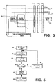
- FIG 3 shows a diagrammatic view of a memory controller 19 embodying the invention together with several memory modules.
- the memory controller 19 of Figure 3 comprises data latches 6 for latching the data coming from the memory modules 3, 4, and 5 on the data bus 2; these memory modules may for instance be comprised of SDRAM modules.
- the data latches 6 are enabled by a strobe signal on an input 9.
- a memory clock signal MEMCLK is present on a clock line 7.
- the strobe signal causes data to be read into the latches 6 every clock cycle, this data being only treated as valid a predetermined number of MEMCLK cycles after assertion of the CTRL signal.
- the memory controller 19 comprises programmable means 20 for producing the strobe signal in a programmed timing relation to the clock signal MEMCLK.
- These programmable means can be used for programming the strobe delay according to the memory configuration, so as to ensure correct data reading relative to the CTRL signal (it being possible to time the strobe signal from the MEMCLK signal because the memory data read signal CTRL is also timed from the MEMCLK signal).
- the means 20 may for instance comprise a programmable delay line connected between the memory clock line 7 and the enabling input 9 of the data latches 6.
- This programmable delay line may comprise a programmable register that determines the delay duration in known manner. This makes the programming of the strobe delay easy to implement, through a simple software programming of one register of the memory controller.
- the range and granularity of the strobe delay may depend on the implementation. As an example, a range of 2 to 10 nanoseconds, and a granularity of 150 picoseconds were found to be sufficient for a memory controller accessing up to 4 memory SDRAM modules, at a clock frequency of 125 MHz. If the programmable means 20 comprise a register of the memory controller the size of this register is determined by the range and granularity of the strobe delay.
- Figure 3 only shows the components of the memory controller necessary for the understanding of the present invention.
- the other components of the memory controller 19 are not represented.
- the memory controller will include circuitry for enabling reading of the data latches 6 only a predetermined number of MEMCLK cycles after assertion of the CTRL and this circuitry is not represented in Figure 3.
- the memory controllers embodying this invention allow programming of the strobe signal delay according to the circumstances, for instance according to memory modules configuration, according to memory load, and so on. It allows the memory controller to run at full speed reliably in any memory configuration, notwithstanding variations in load on the memory bus and the actual configuration of the memory controller.
- the means 20 for deriving the strobe signal are programmed by a delay-programming functional block or unit 25 at power-on of the memory controller, to ensure that any change in the memory configuration is properly taken into account. It is also possible to proceed with the programming whenever a change of the memory configuration is detected.
- the unit 25 for programming the programmable means 20 may take the form of dedicated hardware circuitry provided internally or externally of the memory controller or by a system microprocessor operating under firmware control.
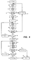
- Figure 4 is a flow chart of a method for programming the strobe signal delay in accordance with the invention.
- the method of Figure 4 is a simple and quick method for programming the means 20 for deriving the strobe signal.
- the means 20 for deriving the strobe signal can be programmed to set a delay ⁇ between the memory clock signal and the strobe signal.
- the delay ⁇ may be programmed in a range ⁇ min - ⁇ max , with a granularity of g.
- the program determines a lowest value ⁇ _ ensuring a correct reading of the data from the memory.
- step 30 the delay ⁇ is set to the minimum value ⁇ min .
- the program proceeds to step 31.
- step 31 data is written into the memory.
- the program proceeds to step 32.
- step 32 data is read from the memory.
- the program proceeds to step 33.
- step 33 the data read from the memory is compared to the data written into the memory. If the data read and written are different, the program proceeds to step 34. If the data read and written are not different, the program proceeds to step 35.
- step 34 the delay is incremented by g.
- the program then proceeds to step 31.
- step 35 ⁇ has a value which has already produced one correct reading of the data in the memory.
- this value is checked in steps 36-41 to ensure that this value of ⁇ gives correct reading of data for more than one operation.
- This reliability test is not compulsory, and may be skipped. In this case, the program proceeds directly to step 42.
- step 36 the reliability of the write/read operation with the current value of ⁇ is checked, by performing i max write and read operations.
- step 36 a parameter i is set at 1. The program proceeds to step 37.
- step 37 data is written into the memory.
- the program proceeds to step 38.
- step 38 data is read from the memory.
- the program proceeds to step 39.
- step 39 the data read from the memory is compared to the data written into the memory. If the data read and written are different, it is determined that the current value of ⁇ is not reliable; the program proceeds to step 34. If the data read and written are the same, the program proceeds to step 40.
- step 41 i is incremented by 1. The program then proceeds to step 37.
- step 42 the current value of ⁇ is stored as ⁇ _; this value of ⁇ is the lowest value for which the reading of the data is successful. The value of ⁇ is then incremented by g. The program then proceeds to step 43.
- steps 43-49 the program determines a value ⁇ + for the delay.
- ⁇ + for the delay.
- data may be read correctly from the memory.
- step 43 data is written into the memory.
- the program proceeds to step 44.
- step 44 data is read from the memory.
- the program proceeds to step 45.
- step 45 the data read from the memory is compared to the data written into the memory. If the data read and written are identical, the program proceeds to step 46. If the data read and written are different, the program proceeds to step 48.
- step 46 it has been determined that the current value of ⁇ is still resulting in at least one correct reading of the data from the memory. It is possible, optionally, to check whether the current value of ⁇ ensures correct reading for more that one write/read operation. This may be done using program steps similar to steps 36-41: however, this reliability test is not compulsory, and may be skipped.
- step 47 the delay ⁇ is incremented by g.
- the program proceeds to step 43.
- step 48 a value of ⁇ giving at least one incorrect reading of the data in the memory has been reached.
- values of ⁇ between ⁇ _ and ⁇ - g i.e. the current value of ⁇ minus one increment ensure correct reading in the memory.
- the value ⁇ - g is stored as ⁇ + . The program then proceeds to step 50.
- step 49 it has been determined that the values of ⁇ between ⁇ - and ⁇ max result in a correct reading of the data in the memory.
- the value ⁇ max is stored as ⁇ + .
- the program then proceeds to step 50.
- step 50 it has been ascertained that values of ⁇ between ⁇ - and ⁇ + result in correct reading of the data.
- the delay ⁇ may then be programmed at any value within this range, e.g. at the value nearest to ( ⁇ + - ⁇ _)/2 .
- the method of Figure 4 allows for a simple and quick setting of the delay ⁇ . Other methods are possible; the method of Figure 4 may also be modified. For instance, in the flow chart of Figure 4, each reading step follows a writing step; the information which is written into the memory may vary for each write/read operation, to ensure correct statistical check of the memory; however, it would also be possible to have only one writing step, and to read always the same data. It is also possible to start by determining ⁇ + , and then determine ⁇ _, the necessary changes being obvious for the person skilled in the art.
- the whole range of delay values is checked to ascertain whether there exist several appropriate reading windows [ ⁇ _; ⁇ + ]; if this is the case, a value of ⁇ in the largest window is preferably chosen.
- Figure 5 shows a flowchart for this method.
- the delay ⁇ is set to the minimum value ⁇ min .
- a parameter j is set to 1.
- the program proceeds to step 61.
- step 61 a reading range or window [ ⁇ - ; ⁇ + ] is determined, e.g. using steps 31-49 of Figure 4.
- the program proceeds to step 62.
- step 62 the current values of ⁇ - and ⁇ + are stored as ⁇ -j and ⁇ +j .
- the program then proceeds to step 63.
- step 63 ⁇ + is compared to ⁇ max . If ⁇ + is equal to ⁇ max , there cannot be any further appropriate window. In this case, the program proceeds to step 65. If this is not the case, the program proceeds to step 64.
- step 64 j is incremented by one, and ⁇ is incremented by g.
- the program then proceeds to step 61.
- step 65 for all possible values of j, the difference ⁇ +j - ⁇ -j is computed. The largest difference is determined. This provides the largest reading window. The program then proceeds to step 66.
- step 66 delay ⁇ is programmed at any value within this largest reading window, e.g. at the value nearest to ( ⁇ +j - ⁇ -j )/2, j being the index of the largest reading window, as determined in step 65.
- the method of Figure 5 ensures that the value for the delay is chosen in the largest possible range appropriate for reading data from the memory.
- the delay-programming unit 25 can be arranged to incrementally adjust the programmed delay value in dependence on variations in supply voltage and/or temperature whereby to compensate for any undesired drifting of the strobe signal during use of the memory controller.
- the unit 25 further comprises means responsive to changes in the measured parameter value over time to determine an appropriate change in the delay set into the programmable delay 20; these means could take the form of a look-up table. Once an appropriate change in delay has been determined, the unit 25 changes the programmed delay by the appropriate amount.
- the simplest way of producing the strobe signal is to delay either the MEMCLK or CTRL signal as described above, it will be appreciated that other ways are possible.
- a separate clock circuit could be used to generate the strobe signal, this clock circuit being synchronised with the MEMCLK signal in a desired phase relation thereto by a suitable phase-locked loop.
Claims (17)
- Ein System, das zumindest ein Speichermodul (3, 4, 5) und eine Speichersteuerung (19) aufweist, wobei die Speichersteuerung folgende Merkmale aufweist:eine Taktleitung (7) für ein Taktsignal;eine Datenempfangseinrichtung (2) zum Verbinden mit dem zumindest einen Speichermodul (3, 4, 5);eine Datenzwischenspeicherungseinrichtung (6), die mit der Datenempfangseinrichtung (2) verbunden ist, zum Zwischenspeichern von Daten unter der Steuerung eines Strobe-Signals; undeine programmierbare Einrichtung (20) zum Liefern des Strobe-Signals in programmierter Zeitgebungsbeziehung zu dem Taktsignal, dadurch gekennzeichnet, dass das System folgende Merkmale aufweist:eine erste Einrichtung zum periodischen Messen des Werts eines Parameters, der die Signalverzögerungscharakteristika in dem System anzeigt, um Abweichungen in demselben zu erfassen, undeine zweite Einrichtung, die auf Abweichungen in den Signalverzögerungscharakteristika anspricht, die durch die erste Einrichtung erfasst werden, um die Programmierung der programmierbaren Einrichtung zu ändern, um die programmierte Zeitgebungsbeziehung für die Abweichungen zu kompensieren.
- Ein System gemäß Anspruch 1, bei dem die programmierbare Einrichtung (20) eine programmierbare Verzögerungseinrichtung aufweist, die wirksam zwischen die Taktleitung (7) und die Datenzwischenspeicherungseinrichtung (6) geschaltet ist.
- Ein System gemäß Anspruch 1, das ferner folgende Merkmale aufweist:wobei die programmierbare Einrichtung (20) eine programmierbare Verzögerungseinrichtung ist, die wirksam zwischen die Speichersteuerungsleitung und die Datenzwischenspeicherungseinrichtung geschaltet ist.eine Speichersteuerungsleitung (8) für ein Speicherlesesignal, undeine Einrichtung zum Erzeugen des Speicherlesesignals in zeitlich abgestimmter Beziehung zu dem Taktsignal;
- Ein System gemäß einem der vorhergehenden Ansprüche, bei dem die programmierbare Einrichtung (20) ein programmierbares Register zum Einstellen der programmierten Zeitgebungsbeziehung aufweist.
- Ein System gemäß Anspruch 4, bei dem die Programmierungseinrichtung das Programmieren nach dem Einschalten des Systems bewirkt.
- Ein System gemäß einem der vorhergehenden Ansprüche, bei dem die programmierbare Einrichtung eine Einrichtung aufweist, die angeordnet ist, um die folgenden Schritte auszuführen:(a) - Programmieren der programmierbaren Einrichtung auf einen gegebenen Wert;(b) - Verwenden der Speichersteuerung zum Schreiben von Daten in die Speichereinrichtung;(c) - Verwenden der Speichersteuerung zum Lesen der Daten, die in die Speichereinrichtung geschrieben sind;(d) - Bestimmen, ob die Daten, die bei Schritt (b) gelesen werden, identisch zu den Daten sind, die bei Schritt (c) geschrieben werden;(e) - Wiederholen der Schritte (a) bis (d), bis Schritt (d) ein positives Ergebnis für zumindest einen gegebenen Wert ergibt;(f) - Programmieren der programmierbaren Einrichtung auf einen des zumindest einen gegebenen Werts.
- Ein System gemäß Anspruch 6, das so angeordnet ist, dass der Schritt (e) das Inkrementieren des gegebenen Werts aufweist, und sobald Schritt (d) ein positives Ergebnis ergeben hat, Schritte (a) bis (d) wiederholt werden, bis Schritt (d) ein negatives Ergebnis ergibt.
- Ein System gemäß Anspruch 6, das so angeordnet ist, dass Schritt (e) das Dekrementieren des gegebenen Werts aufweist, und sobald Schritt (d) ein positives Ergebnis ergeben hat, Schritte (a) bis (d) wiederholt werden, bis Schritt (d) ein negatives Ergebnis ergibt.
- Ein System gemäß Anspruch 7 oder Anspruch 8, das so angeordnet ist, dass Schritt (f) das Auswählen eines Werts in einem Bereich von Werten aufweist, für die Schritt (d) ein positives Ergebnis ergibt.
- Ein System gemäß Anspruch 6, das so angeordnet ist, dass Schritt (e) für alle möglichen programmierbaren Werte wiederholt wird.
- Ein System gemäß Anspruch 10, das so angeordnet ist, dass Schritt (f) Folgendes aufweist:und bei dem die programmierbare Einrichtung auf einen Wert programmiert ist, der in dem größten der Bereiche enthalten ist.(g) Bestimmen von Bereichen von Werten, für die Schritt (d) ein positives Ergebnis ergibt;(h) Bestimmen des größten dieser Bereiche von Werten;
- Ein Verfahren zum Verbessern der Zuverlässigkeit des Lesens von Daten in einer Speichersteuerung aus zumindest einem Speichermodul innerhalb eines Systems, wobei die Speichersteuerung eine Datenempfangseinrichtung (2) zum Verbinden mit dem zumindest einen Speichermodul (3, 4, 5) und eine Datenzwischenspeicherungseinrichtung (6), die mit der Datenempfangseinrichtung (2) verbunden ist, aufweist, zum Zwischenspeichern von Daten unter der Steuerung des Lese-Strobe-Signals, wobei das Verfahren folgenden Schritt aufweist:wobei das Verfahren durch folgende Schritte gekennzeichnet ist:Programmieren in einer programmierbaren Einrichtung innerhalb der Speichersteuerung einer Verzögerung zwischen einem Taktsignal (10) und einem Lese-Strobe-Signal aufweist;periodisches Messen des Werts eines Parameters, der die Signalverzögerungscharakteristika in dem System anzeigt, um Abweichungen in demselben zu erfassen; undAnsprechen auf Abweichungen bei den Signalverzögerungscharakteristika, die durch die erste Einrichtung erfasst werden, um die Programmierung der Verzögerung zu ändern, um die programmierte Zeitgebungsbeziehung für die Abweichungen zu kompensieren.
- Ein Verfahren gemäß Anspruch 12, bei dem das Programmieren beim Einschalten der Speichersteuerung ausgeführt wird.
- Ein Verfahren gemäß Anspruch 12, bei dem das Programmieren ausgeführt wird, um Spannungsabweichungen zu kompensieren.
- Ein Verfahren gemäß Anspruch 12, bei dem das Programmieren ausgeführt wird, um Abweichungen bei der Verarbeitungslast zu kompensieren.
- Ein Verfahren gemäß Anspruch 12, bei dem das Programmieren ausgeführt wird, um Temperaturabweichungen zu kompensieren.
Priority Applications (3)
| Application Number | Priority Date | Filing Date | Title |
|---|---|---|---|
| DE69731066T DE69731066T2 (de) | 1997-01-23 | 1997-01-23 | Speichersteuerungsvorrichtung mit programmierbarer Impulsverzögerung |
| EP97410009A EP0855653B1 (de) | 1997-01-23 | 1997-01-23 | Speichersteuerungsvorrichtung mit programmierbarer Impulsverzögerung |
| JP10004583A JPH10232818A (ja) | 1997-01-23 | 1998-01-13 | メモリ・コントローラ |
Applications Claiming Priority (1)
| Application Number | Priority Date | Filing Date | Title |
|---|---|---|---|
| EP97410009A EP0855653B1 (de) | 1997-01-23 | 1997-01-23 | Speichersteuerungsvorrichtung mit programmierbarer Impulsverzögerung |
Publications (2)
| Publication Number | Publication Date |
|---|---|
| EP0855653A1 EP0855653A1 (de) | 1998-07-29 |
| EP0855653B1 true EP0855653B1 (de) | 2004-10-06 |
Family
ID=8229944
Family Applications (1)
| Application Number | Title | Priority Date | Filing Date |
|---|---|---|---|
| EP97410009A Expired - Lifetime EP0855653B1 (de) | 1997-01-23 | 1997-01-23 | Speichersteuerungsvorrichtung mit programmierbarer Impulsverzögerung |
Country Status (3)
| Country | Link |
|---|---|
| EP (1) | EP0855653B1 (de) |
| JP (1) | JPH10232818A (de) |
| DE (1) | DE69731066T2 (de) |
Cited By (6)
| Publication number | Priority date | Publication date | Assignee | Title |
|---|---|---|---|---|
| EP2014883A2 (de) | 2003-05-10 | 2009-01-14 | Universität Stuttgart | Verfahren und Vorrichtung zur Reinigung von Abgasen |
| US8214616B2 (en) | 2001-04-24 | 2012-07-03 | Rambus Inc. | Memory controller device having timing offset capability |
| US8214575B2 (en) | 1997-09-26 | 2012-07-03 | Rambus Inc. | Memory module having signal lines configured for sequential arrival of signals at synchronous memory devices |
| US8283955B2 (en) | 2006-03-13 | 2012-10-09 | Nxp B.V. | Double data rate interface |
| US8320202B2 (en) | 2001-04-24 | 2012-11-27 | Rambus Inc. | Clocked memory system with termination component |
| US9229470B2 (en) | 2004-09-15 | 2016-01-05 | Rambus Inc. | Memory controller with clock-to-strobe skew compensation |
Families Citing this family (12)
| Publication number | Priority date | Publication date | Assignee | Title |
|---|---|---|---|---|
| US7050959B1 (en) | 1999-12-23 | 2006-05-23 | Intel Corporation | Dynamic thermal management for integrated circuits |
| US6578125B2 (en) * | 2000-02-14 | 2003-06-10 | Sanyo Electric Co., Ltd. | Memory access circuit and memory access control circuit |
| JP2001337862A (ja) * | 2000-05-29 | 2001-12-07 | Fujitsu Ltd | メモリシステム及びそのセットアップ方法 |
| WO2002001363A1 (fr) * | 2000-06-27 | 2002-01-03 | Matsushita Electric Industrial, Co., Ltd. | Dispositif et procede de commande de memoire |
| KR100389916B1 (ko) * | 2000-08-28 | 2003-07-04 | 삼성전자주식회사 | 메모리 모듈 및 메모리 컨트롤러 |
| US6553472B2 (en) | 2001-01-12 | 2003-04-22 | Sun Microsystems, Inc. | Method for programming clock delays, command delays, read command parameter delays, and write command parameter delays of a memory controller in a high performance microprocessor |
| EP1291778B1 (de) * | 2001-04-24 | 2007-06-27 | Rambus Inc. | Verfahren und Gerät zum Koordinieren von Speicheroperationen zwischen unterschiedlich angeordneten Speicherkomponenten |
| US6697926B2 (en) | 2001-06-06 | 2004-02-24 | Micron Technology, Inc. | Method and apparatus for determining actual write latency and accurately aligning the start of data capture with the arrival of data at a memory device |
| US6918048B2 (en) | 2001-06-28 | 2005-07-12 | Intel Corporation | System and method for delaying a strobe signal based on a slave delay base and a master delay adjustment |
| US20040215912A1 (en) * | 2003-04-24 | 2004-10-28 | George Vergis | Method and apparatus to establish, report and adjust system memory usage |
| US7966439B1 (en) * | 2004-11-24 | 2011-06-21 | Nvidia Corporation | Apparatus, system, and method for a fast data return memory controller |
| US20100312981A1 (en) * | 2008-01-29 | 2010-12-09 | Panasonic Corporation | Memory access timing adjustment device and memory access timing adjustment method |
Citations (1)
| Publication number | Priority date | Publication date | Assignee | Title |
|---|---|---|---|---|
| WO1997015897A1 (en) * | 1995-10-26 | 1997-05-01 | Motorola Inc. | Method and device for encoding/decoding a displaced frame difference |
Family Cites Families (4)
| Publication number | Priority date | Publication date | Assignee | Title |
|---|---|---|---|---|
| US5335337A (en) * | 1989-01-27 | 1994-08-02 | Digital Equipment Corporation | Programmable data transfer timing |
| US5608896A (en) * | 1992-05-28 | 1997-03-04 | Texas Instruments Incorporated | Time skewing arrangement for operating memory devices in synchronism with a data processor |
| US5509138A (en) * | 1993-03-22 | 1996-04-16 | Compaq Computer Corporation | Method for determining speeds of memory modules |
| US5557782A (en) * | 1994-07-12 | 1996-09-17 | Zenith Data Systems Corporation | Flexible deterministic state machine |
-
1997
- 1997-01-23 EP EP97410009A patent/EP0855653B1/de not_active Expired - Lifetime
- 1997-01-23 DE DE69731066T patent/DE69731066T2/de not_active Expired - Fee Related
-
1998
- 1998-01-13 JP JP10004583A patent/JPH10232818A/ja active Pending
Patent Citations (1)
| Publication number | Priority date | Publication date | Assignee | Title |
|---|---|---|---|---|
| WO1997015897A1 (en) * | 1995-10-26 | 1997-05-01 | Motorola Inc. | Method and device for encoding/decoding a displaced frame difference |
Cited By (19)
| Publication number | Priority date | Publication date | Assignee | Title |
|---|---|---|---|---|
| US8214575B2 (en) | 1997-09-26 | 2012-07-03 | Rambus Inc. | Memory module having signal lines configured for sequential arrival of signals at synchronous memory devices |
| US8364878B2 (en) | 1997-09-26 | 2013-01-29 | Rambus Inc. | Memory module having signal lines configured for sequential arrival of signals at a plurality of memory devices |
| US8395951B2 (en) | 2001-04-24 | 2013-03-12 | Rambus Inc. | Memory controller |
| US8625371B2 (en) | 2001-04-24 | 2014-01-07 | Rambus Inc. | Memory component with terminated and unterminated signaling inputs |
| US8320202B2 (en) | 2001-04-24 | 2012-11-27 | Rambus Inc. | Clocked memory system with termination component |
| US8359445B2 (en) | 2001-04-24 | 2013-01-22 | Rambus Inc. | Method and apparatus for signaling between devices of a memory system |
| US8214616B2 (en) | 2001-04-24 | 2012-07-03 | Rambus Inc. | Memory controller device having timing offset capability |
| US8391039B2 (en) | 2001-04-24 | 2013-03-05 | Rambus Inc. | Memory module with termination component |
| US9472262B2 (en) | 2001-04-24 | 2016-10-18 | Rambus Inc. | Memory controller |
| US8462566B2 (en) | 2001-04-24 | 2013-06-11 | Rambus Inc. | Memory module with termination component |
| US8537601B2 (en) | 2001-04-24 | 2013-09-17 | Rambus Inc. | Memory controller with selective data transmission delay |
| US9311976B2 (en) | 2001-04-24 | 2016-04-12 | Rambus Inc. | Memory module |
| US8717837B2 (en) | 2001-04-24 | 2014-05-06 | Rambus Inc. | Memory module |
| US8760944B2 (en) | 2001-04-24 | 2014-06-24 | Rambus Inc. | Memory component that samples command/address signals in response to both edges of a clock signal |
| US9053778B2 (en) | 2001-04-24 | 2015-06-09 | Rambus Inc. | Memory controller that enforces strobe-to-strobe timing offset |
| EP2014883A2 (de) | 2003-05-10 | 2009-01-14 | Universität Stuttgart | Verfahren und Vorrichtung zur Reinigung von Abgasen |
| US9229470B2 (en) | 2004-09-15 | 2016-01-05 | Rambus Inc. | Memory controller with clock-to-strobe skew compensation |
| US9437279B2 (en) | 2004-09-15 | 2016-09-06 | Rambus Inc. | Memory controller with clock-to-strobe skew compensation |
| US8283955B2 (en) | 2006-03-13 | 2012-10-09 | Nxp B.V. | Double data rate interface |
Also Published As
| Publication number | Publication date |
|---|---|
| EP0855653A1 (de) | 1998-07-29 |
| JPH10232818A (ja) | 1998-09-02 |
| DE69731066D1 (de) | 2004-11-11 |
| DE69731066T2 (de) | 2005-10-06 |
Similar Documents
| Publication | Publication Date | Title |
|---|---|---|
| EP0855653B1 (de) | Speichersteuerungsvorrichtung mit programmierbarer Impulsverzögerung | |
| US5495593A (en) | Microcontroller device having remotely programmable EPROM and method for programming | |
| US6851016B2 (en) | System latency levelization for read data | |
| US6316980B1 (en) | Calibrating data strobe signal using adjustable delays with feedback | |
| US6456544B1 (en) | Selective forwarding of a strobe based on a predetermined delay following a memory read command | |
| US7145374B2 (en) | Methods and apparatus for delay circuit | |
| EP0897154A2 (de) | Speichersteuerungsvorrichtung zur Unterstützung von DRAM-Schaltungen mit verschiedenen Betriebsgeschwindigkeiten | |
| CN102347081A (zh) | 用于ddr控制器中dqs延迟的相位校准方法及装置 | |
| JP5577776B2 (ja) | メモリ制御装置及びマスクタイミング制御方法 | |
| US5870404A (en) | Self-timed circuit having critical path timing detection | |
| JP2006040518A (ja) | データ出力時にddr動作を行う不揮発性メモリ装置及びデータ出力方法 | |
| US7796465B2 (en) | Write leveling of memory units designed to receive access requests in a sequential chained topology | |
| CN101232363B (zh) | 相位调节功能评估方法,传输容限测量方法以及信息处理装置 | |
| US5305277A (en) | Data processing apparatus having address decoder supporting wide range of operational frequencies | |
| KR100532973B1 (ko) | 메모리 장치의 데이타 출력 드라이버 제어 장치 | |
| US6968436B2 (en) | Memory controller that controls supply timing of read data | |
| JPH027530B2 (de) | ||
| KR20080005294A (ko) | 라이브 측정으로 측정-초기화되는 지연 고정 루프 | |
| US5235699A (en) | Timing calibrate and track control circuit | |
| KR102547449B1 (ko) | 실리콘 웨이퍼 상의 집적 회로용 테스터 및 집적 회로 | |
| JP3039631B2 (ja) | 信号線監視装置 | |
| JPH0143392B2 (de) | ||
| JP2588528B2 (ja) | メモリ実装検出回路 | |
| JPH11316619A (ja) | クロックスキュー調整回路 | |
| KR100415086B1 (ko) | 플래쉬 메모리를 내장한 마이크로 콘트롤러 장치 및 그제어 방법 |
Legal Events
| Date | Code | Title | Description |
|---|---|---|---|
| PUAI | Public reference made under article 153(3) epc to a published international application that has entered the european phase |
Free format text: ORIGINAL CODE: 0009012 |
|
| AK | Designated contracting states |
Kind code of ref document: A1 Designated state(s): DE FR GB |
|
| AX | Request for extension of the european patent |
Free format text: AL;LT;LV;RO;SI |
|
| 17P | Request for examination filed |
Effective date: 19990102 |
|
| AKX | Designation fees paid |
Free format text: DE FR GB |
|
| RBV | Designated contracting states (corrected) |
Designated state(s): DE FR GB |
|
| RAP1 | Party data changed (applicant data changed or rights of an application transferred) |
Owner name: HEWLETT-PACKARD COMPANY, A DELAWARE CORPORATION |
|
| 17Q | First examination report despatched |
Effective date: 20031215 |
|
| GRAP | Despatch of communication of intention to grant a patent |
Free format text: ORIGINAL CODE: EPIDOSNIGR1 |
|
| GRAS | Grant fee paid |
Free format text: ORIGINAL CODE: EPIDOSNIGR3 |
|
| GRAA | (expected) grant |
Free format text: ORIGINAL CODE: 0009210 |
|
| AK | Designated contracting states |
Kind code of ref document: B1 Designated state(s): DE FR GB |
|
| REG | Reference to a national code |
Ref country code: GB Ref legal event code: FG4D |
|
| REF | Corresponds to: |
Ref document number: 69731066 Country of ref document: DE Date of ref document: 20041111 Kind code of ref document: P |
|
| ET | Fr: translation filed | ||
| PLBE | No opposition filed within time limit |
Free format text: ORIGINAL CODE: 0009261 |
|
| STAA | Information on the status of an ep patent application or granted ep patent |
Free format text: STATUS: NO OPPOSITION FILED WITHIN TIME LIMIT |
|
| 26N | No opposition filed |
Effective date: 20050707 |
|
| PGFP | Annual fee paid to national office [announced via postgrant information from national office to epo] |
Ref country code: GB Payment date: 20070125 Year of fee payment: 11 |
|
| PGFP | Annual fee paid to national office [announced via postgrant information from national office to epo] |
Ref country code: DE Payment date: 20070228 Year of fee payment: 11 |
|
| PGFP | Annual fee paid to national office [announced via postgrant information from national office to epo] |
Ref country code: FR Payment date: 20070207 Year of fee payment: 11 |
|
| GBPC | Gb: european patent ceased through non-payment of renewal fee |
Effective date: 20080123 |
|
| PG25 | Lapsed in a contracting state [announced via postgrant information from national office to epo] |
Ref country code: DE Free format text: LAPSE BECAUSE OF NON-PAYMENT OF DUE FEES Effective date: 20080801 |
|
| REG | Reference to a national code |
Ref country code: FR Ref legal event code: ST Effective date: 20081029 |
|
| PG25 | Lapsed in a contracting state [announced via postgrant information from national office to epo] |
Ref country code: GB Free format text: LAPSE BECAUSE OF NON-PAYMENT OF DUE FEES Effective date: 20080123 |
|
| PG25 | Lapsed in a contracting state [announced via postgrant information from national office to epo] |
Ref country code: FR Free format text: LAPSE BECAUSE OF NON-PAYMENT OF DUE FEES Effective date: 20080131 |