EP0852807B1 - Verfahren zum elektrischen verbinden eines halbleiterchips mit zumindest einer kontaktfläche - Google Patents
Verfahren zum elektrischen verbinden eines halbleiterchips mit zumindest einer kontaktfläche Download PDFInfo
- Publication number
- EP0852807B1 EP0852807B1 EP96937189A EP96937189A EP0852807B1 EP 0852807 B1 EP0852807 B1 EP 0852807B1 EP 96937189 A EP96937189 A EP 96937189A EP 96937189 A EP96937189 A EP 96937189A EP 0852807 B1 EP0852807 B1 EP 0852807B1
- Authority
- EP
- European Patent Office
- Prior art keywords
- contact
- semiconductor chip
- wedge
- nailhead
- wire
- Prior art date
- Legal status (The legal status is an assumption and is not a legal conclusion. Google has not performed a legal analysis and makes no representation as to the accuracy of the status listed.)
- Expired - Lifetime
Links
Images

Classifications
-
- H—ELECTRICITY
- H10—SEMICONDUCTOR DEVICES; ELECTRIC SOLID-STATE DEVICES NOT OTHERWISE PROVIDED FOR
- H10W—GENERIC PACKAGES, INTERCONNECTIONS, CONNECTORS OR OTHER CONSTRUCTIONAL DETAILS OF DEVICES COVERED BY CLASS H10
- H10W72/00—Interconnections or connectors in packages
- H10W72/071—Connecting or disconnecting
- H10W72/072—Connecting or disconnecting of bump connectors
- H10W72/07231—Techniques
- H10W72/07232—Compression bonding, e.g. thermocompression bonding
- H10W72/07233—Ultrasonic bonding, e.g. thermosonic bonding
-
- B—PERFORMING OPERATIONS; TRANSPORTING
- B23—MACHINE TOOLS; METAL-WORKING NOT OTHERWISE PROVIDED FOR
- B23K—SOLDERING OR UNSOLDERING; WELDING; CLADDING OR PLATING BY SOLDERING OR WELDING; CUTTING BY APPLYING HEAT LOCALLY, e.g. FLAME CUTTING; WORKING BY LASER BEAM
- B23K20/00—Non-electric welding by applying impact or other pressure, with or without the application of heat, e.g. cladding or plating
- B23K20/002—Non-electric welding by applying impact or other pressure, with or without the application of heat, e.g. cladding or plating specially adapted for particular articles or work
- B23K20/004—Wire welding
- B23K20/005—Capillary welding
- B23K20/007—Ball bonding
-
- H—ELECTRICITY
- H10—SEMICONDUCTOR DEVICES; ELECTRIC SOLID-STATE DEVICES NOT OTHERWISE PROVIDED FOR
- H10W—GENERIC PACKAGES, INTERCONNECTIONS, CONNECTORS OR OTHER CONSTRUCTIONAL DETAILS OF DEVICES COVERED BY CLASS H10
- H10W72/00—Interconnections or connectors in packages
- H10W72/01—Manufacture or treatment
- H10W72/012—Manufacture or treatment of bump connectors, dummy bumps or thermal bumps
- H10W72/01221—Manufacture or treatment of bump connectors, dummy bumps or thermal bumps using local deposition
- H10W72/01225—Manufacture or treatment of bump connectors, dummy bumps or thermal bumps using local deposition in solid form, e.g. by using a powder or by stud bumping
-
- H—ELECTRICITY
- H10—SEMICONDUCTOR DEVICES; ELECTRIC SOLID-STATE DEVICES NOT OTHERWISE PROVIDED FOR
- H10W—GENERIC PACKAGES, INTERCONNECTIONS, CONNECTORS OR OTHER CONSTRUCTIONAL DETAILS OF DEVICES COVERED BY CLASS H10
- H10W72/00—Interconnections or connectors in packages
- H10W72/071—Connecting or disconnecting
- H10W72/0711—Apparatus therefor
- H10W72/07141—Means for applying energy, e.g. ovens or lasers
-
- H—ELECTRICITY
- H10—SEMICONDUCTOR DEVICES; ELECTRIC SOLID-STATE DEVICES NOT OTHERWISE PROVIDED FOR
- H10W—GENERIC PACKAGES, INTERCONNECTIONS, CONNECTORS OR OTHER CONSTRUCTIONAL DETAILS OF DEVICES COVERED BY CLASS H10
- H10W72/00—Interconnections or connectors in packages
- H10W72/071—Connecting or disconnecting
- H10W72/075—Connecting or disconnecting of bond wires
-
- H—ELECTRICITY
- H10—SEMICONDUCTOR DEVICES; ELECTRIC SOLID-STATE DEVICES NOT OTHERWISE PROVIDED FOR
- H10W—GENERIC PACKAGES, INTERCONNECTIONS, CONNECTORS OR OTHER CONSTRUCTIONAL DETAILS OF DEVICES COVERED BY CLASS H10
- H10W72/00—Interconnections or connectors in packages
- H10W72/071—Connecting or disconnecting
- H10W72/075—Connecting or disconnecting of bond wires
- H10W72/07511—Treating the bonding area before connecting, e.g. by applying flux or cleaning
-
- H—ELECTRICITY
- H10—SEMICONDUCTOR DEVICES; ELECTRIC SOLID-STATE DEVICES NOT OTHERWISE PROVIDED FOR
- H10W—GENERIC PACKAGES, INTERCONNECTIONS, CONNECTORS OR OTHER CONSTRUCTIONAL DETAILS OF DEVICES COVERED BY CLASS H10
- H10W72/00—Interconnections or connectors in packages
- H10W72/071—Connecting or disconnecting
- H10W72/075—Connecting or disconnecting of bond wires
- H10W72/07521—Aligning
-
- H—ELECTRICITY
- H10—SEMICONDUCTOR DEVICES; ELECTRIC SOLID-STATE DEVICES NOT OTHERWISE PROVIDED FOR
- H10W—GENERIC PACKAGES, INTERCONNECTIONS, CONNECTORS OR OTHER CONSTRUCTIONAL DETAILS OF DEVICES COVERED BY CLASS H10
- H10W72/00—Interconnections or connectors in packages
- H10W72/071—Connecting or disconnecting
- H10W72/075—Connecting or disconnecting of bond wires
- H10W72/07531—Techniques
- H10W72/07532—Compression bonding, e.g. thermocompression bonding
- H10W72/07533—Ultrasonic bonding, e.g. thermosonic bonding
-
- H—ELECTRICITY
- H10—SEMICONDUCTOR DEVICES; ELECTRIC SOLID-STATE DEVICES NOT OTHERWISE PROVIDED FOR
- H10W—GENERIC PACKAGES, INTERCONNECTIONS, CONNECTORS OR OTHER CONSTRUCTIONAL DETAILS OF DEVICES COVERED BY CLASS H10
- H10W72/00—Interconnections or connectors in packages
- H10W72/20—Bump connectors, e.g. solder bumps or copper pillars; Dummy bumps; Thermal bumps
- H10W72/251—Materials
-
- H—ELECTRICITY
- H10—SEMICONDUCTOR DEVICES; ELECTRIC SOLID-STATE DEVICES NOT OTHERWISE PROVIDED FOR
- H10W—GENERIC PACKAGES, INTERCONNECTIONS, CONNECTORS OR OTHER CONSTRUCTIONAL DETAILS OF DEVICES COVERED BY CLASS H10
- H10W72/00—Interconnections or connectors in packages
- H10W72/20—Bump connectors, e.g. solder bumps or copper pillars; Dummy bumps; Thermal bumps
- H10W72/29—Bond pads specially adapted therefor
-
- H—ELECTRICITY
- H10—SEMICONDUCTOR DEVICES; ELECTRIC SOLID-STATE DEVICES NOT OTHERWISE PROVIDED FOR
- H10W—GENERIC PACKAGES, INTERCONNECTIONS, CONNECTORS OR OTHER CONSTRUCTIONAL DETAILS OF DEVICES COVERED BY CLASS H10
- H10W72/00—Interconnections or connectors in packages
- H10W72/50—Bond wires
- H10W72/531—Shapes of wire connectors
- H10W72/536—Shapes of wire connectors the connected ends being ball-shaped
-
- H—ELECTRICITY
- H10—SEMICONDUCTOR DEVICES; ELECTRIC SOLID-STATE DEVICES NOT OTHERWISE PROVIDED FOR
- H10W—GENERIC PACKAGES, INTERCONNECTIONS, CONNECTORS OR OTHER CONSTRUCTIONAL DETAILS OF DEVICES COVERED BY CLASS H10
- H10W72/00—Interconnections or connectors in packages
- H10W72/50—Bond wires
- H10W72/531—Shapes of wire connectors
- H10W72/5363—Shapes of wire connectors the connected ends being wedge-shaped
-
- H—ELECTRICITY
- H10—SEMICONDUCTOR DEVICES; ELECTRIC SOLID-STATE DEVICES NOT OTHERWISE PROVIDED FOR
- H10W—GENERIC PACKAGES, INTERCONNECTIONS, CONNECTORS OR OTHER CONSTRUCTIONAL DETAILS OF DEVICES COVERED BY CLASS H10
- H10W72/00—Interconnections or connectors in packages
- H10W72/50—Bond wires
- H10W72/531—Shapes of wire connectors
- H10W72/5366—Shapes of wire connectors the bond wires having kinks
-
- H—ELECTRICITY
- H10—SEMICONDUCTOR DEVICES; ELECTRIC SOLID-STATE DEVICES NOT OTHERWISE PROVIDED FOR
- H10W—GENERIC PACKAGES, INTERCONNECTIONS, CONNECTORS OR OTHER CONSTRUCTIONAL DETAILS OF DEVICES COVERED BY CLASS H10
- H10W72/00—Interconnections or connectors in packages
- H10W72/50—Bond wires
- H10W72/541—Dispositions of bond wires
- H10W72/5434—Dispositions of bond wires the connected ends being on auxiliary connecting means on bond pads, e.g. on other bond wires
-
- H—ELECTRICITY
- H10—SEMICONDUCTOR DEVICES; ELECTRIC SOLID-STATE DEVICES NOT OTHERWISE PROVIDED FOR
- H10W—GENERIC PACKAGES, INTERCONNECTIONS, CONNECTORS OR OTHER CONSTRUCTIONAL DETAILS OF DEVICES COVERED BY CLASS H10
- H10W72/00—Interconnections or connectors in packages
- H10W72/50—Bond wires
- H10W72/541—Dispositions of bond wires
- H10W72/547—Dispositions of multiple bond wires
-
- H—ELECTRICITY
- H10—SEMICONDUCTOR DEVICES; ELECTRIC SOLID-STATE DEVICES NOT OTHERWISE PROVIDED FOR
- H10W—GENERIC PACKAGES, INTERCONNECTIONS, CONNECTORS OR OTHER CONSTRUCTIONAL DETAILS OF DEVICES COVERED BY CLASS H10
- H10W72/00—Interconnections or connectors in packages
- H10W72/50—Bond wires
- H10W72/551—Materials of bond wires
- H10W72/552—Materials of bond wires comprising metals or metalloids, e.g. silver
- H10W72/5522—Materials of bond wires comprising metals or metalloids, e.g. silver comprising gold [Au]
-
- H—ELECTRICITY
- H10—SEMICONDUCTOR DEVICES; ELECTRIC SOLID-STATE DEVICES NOT OTHERWISE PROVIDED FOR
- H10W—GENERIC PACKAGES, INTERCONNECTIONS, CONNECTORS OR OTHER CONSTRUCTIONAL DETAILS OF DEVICES COVERED BY CLASS H10
- H10W72/00—Interconnections or connectors in packages
- H10W72/50—Bond wires
- H10W72/59—Bond pads specially adapted therefor
-
- H—ELECTRICITY
- H10—SEMICONDUCTOR DEVICES; ELECTRIC SOLID-STATE DEVICES NOT OTHERWISE PROVIDED FOR
- H10W—GENERIC PACKAGES, INTERCONNECTIONS, CONNECTORS OR OTHER CONSTRUCTIONAL DETAILS OF DEVICES COVERED BY CLASS H10
- H10W72/00—Interconnections or connectors in packages
- H10W72/90—Bond pads, in general
- H10W72/951—Materials of bond pads
- H10W72/952—Materials of bond pads comprising metals or metalloids, e.g. PbSn, Ag or Cu
-
- H—ELECTRICITY
- H10—SEMICONDUCTOR DEVICES; ELECTRIC SOLID-STATE DEVICES NOT OTHERWISE PROVIDED FOR
- H10W—GENERIC PACKAGES, INTERCONNECTIONS, CONNECTORS OR OTHER CONSTRUCTIONAL DETAILS OF DEVICES COVERED BY CLASS H10
- H10W90/00—Package configurations
- H10W90/701—Package configurations characterised by the relative positions of pads or connectors relative to package parts
- H10W90/751—Package configurations characterised by the relative positions of pads or connectors relative to package parts of bond wires
- H10W90/754—Package configurations characterised by the relative positions of pads or connectors relative to package parts of bond wires between a chip and a stacked insulating package substrate, interposer or RDL
Definitions
- the invention relates to a method for the electrical connection of a semiconductor chip having at least one contact surface by means of a thin wire, the first end with the at least one contact surface and the second end is welded to a arranged on a contact field of the semiconductor chip and conductively connected thereto metal piece.
- Such methods are carried out in a known manner by bonding. It is customary to lead the mostly about 24 micron thick gold wire in a capillary, at the end of which he stands out a piece. By means of a hydrogen flame or an electrically ignited spark the protruding piece is melted, so that it forms a small ball, the so-called ball. This ball is now pressed by means of the capillary on a first contact surface and thereby connected by vibrations of the capillary in the ultrasonic range with the contact surface, wherein a designated nailhead shape of the gold wire is formed. In so-called thermo-sonic bonding, the contact surface is additionally heated to a temperature of about 200 ° C. to 300 ° C.
- the capillary is again moved upwards and guided in an arc, the so-called loop, to a second contact surface which is to be connected to the first contact surface.
- the capillary lowers again and squeezes the gold wire on the second contact surface.
- the relatively high pressure results in a good connection of the gold wire with the second contact surface, resulting in a wedge-shaped wedge-shaped structure.
- This type of bonding is also called ball-wedge bonding, as opposed to wedge-wedge bonding, which is common in aluminum wire.
- the ball When connecting semiconductor chips with contact surfaces, the ball is usually connected to the semiconductor chip and the wedge to the contact surface, since the ball can be better placed and the resulting nailhead has a more precisely defined size than the wedge.
- the risk of destroying structures on the semiconductor chip is very low in the ball-on-chip process.
- the disadvantage of this approach is that the loop turns out to be relatively large, which, however, plays no role in the usual semiconductor packages.
- the housing height which corresponds to the thickness of the chip card, but very small and fixed. If there is a component, such as the carrier, made a little thicker, this additional space needs to be saved elsewhere again.
- e'e EP 0 397 426 A2 discloses an arrangement in which prior to attaching a wedge contact on a contact surface of the semiconductor chip, a nailhead contact is applied to this contact surface and the wedge contact only on this nailhead contact comes. This increases the reliability of the connection.
- the nailhead contact provides the same metallurgical ratios as traditional thermo-sonic nailhead bonding.
- the bonding wire may come into contact with the edge of the semiconductor chip, which may lead to a short circuit.
- the JP 4 294 552 A discloses a bonding wire manufacturing method in which a gold ball is first squeezed onto an aluminum contact surface so that during the application of a bonding wire to the gold ball, the capillaries of the contact surface are not touched.
- the JP 61 023 329 A discloses a method in which a bonding wire is used to form a gold bump on a contact surface.
- the EP 0 320 244 A discloses a substrate having bumps wherein the bumps are formed from a bond wire carried in a sling.
- the EP 0 211 360 discloses a smart card wherein a semiconductor chip is electrically connected via Bonn wires to a redistribution structure.
- the problem of the present invention is thus to provide a method for electrically connecting a semiconductor chip having at least one contact surface, in which a suitable guidance of the bonding wire is ensured with a simple assembly method.
- the wedge-shaped piece of metal which is formed by a nailhead contact whose free end is guided in a loop and connected as a wedge-contact with the nailhead, the loop of the semiconductor chip with the contact surface connecting bonding wire from the surface of the semiconductor chip in the direction of the chip edge obliquely upward, so that no contact with the edge can come about.
- a gold wire of about 24 microns diameter is guided by means of a capillary 4 on a designated contact field on a semiconductor chip 1.
- a ball At the end of the capillary had formed by short-term liquefaction of the gold wire, a ball, the so-called ball.
- the arrow indicates the direction of movement of the capillary 4.
- the ball was pressed onto the contact field and formed into the nailhead 6.
- a thermo-sonic method was used.
- the capillary 4 moves with the gold wire in a loop and squeezes the free end on the nailhead 6 from which the loop is deformed into a wedge 7.
- the end of the gold wire is then melted back into a ball.
- a wedge-shaped metal piece 5 consisting of a nailhead contact 6 and a crimped wire loop 7 was formed in this way.
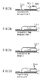
- FIG. 2 shows a section of a chip card module.
- a chip card module is inserted into a recess of a plastic card, whereby one obtains a chip card.
- a glass epoxy plate 3 is provided on one side with a copper laminate 2 and forms a carrier.
- the glass epoxy 3 of Carrier is a hole for a contact surface attached.
- the chip 1 is glued to the glass epoxy 3.
- the gold wire for connecting the semiconductor chip 1 with a contact surface is still guided almost parallel to the semiconductor chip surface, so that the gold wire has a small loop height, through which the chip surface easily
- increasing the lead of the wire eliminates the risk of touching the wire with the chip edge.
- this method Compared with the aluminum wedge bonding method, which also allows for very low loop heights, this method has the advantage that the time to pull a wire is much shorter (about a factor of 2).
- the method according to the invention can also be used or applied equivalently in differently constructed carriers for chip card modules and also in other housing variants for semiconductor components.
Landscapes
- Engineering & Computer Science (AREA)
- Mechanical Engineering (AREA)
- Wire Bonding (AREA)
- Credit Cards Or The Like (AREA)
Description
- Die Erfindung betrifft ein Verfahren zur elektrischen Verbindung eines Halbleiterchips mit zumindest einer Kontaktfläche mittels eines dünnen Drahtes, dessen erstes Ende mit der zumindest einen Kontaktfläche und dessen zweites Ende mit einem auf einem Kontaktfeld des Halbleiterchips angeordneten und mit diesem leitend verbundenen Metallstück verschweißt ist.
- Solche Verfahren werden in bekannter Weise durch Bonden durchgeführt. Es ist dabei üblich, den meistens etwa 24 µm dicken Golddraht in einer Kapillare zu führen, an deren Ende er ein Stück heraussteht. Mittels einer Wasserstoffflamme oder eines elektrisch gezündeten Funkens wird das herausstehende Stück geschmolzen, so daß es sich zu einer kleinen Kugel, dem sogenannten ball formt. Diese Kugel wird nun mittels der Kapillare auf eine erste Kontaktfläche gedrückt und dabei durch Vibrationen der Kapillare im Ultraschallbereich mit der Kontaktfläche verbunden, wobei eine als nailhead bezeichnete Form des Golddrahtes entsteht. Beim sogenannten thermo-sonic-Bonden wird zusätzlich die Kontaktfläche auf eine Temperatur von etwa 200° C bis 300° C aufgeheizt. Danach wird die Kapillare wieder nach oben bewegt und in einem Bogen, dem sogenannten loop, zu einer zweiten Kontaktfläche, die mit der ersten Kontaktfläche verbunden werden soll, geführt. Dort senkt sich die Kapillare wieder ab und quetscht den Golddraht auf der zweiten Kontaktfläche ab. Durch den relativ hohen Druck entsteht eine gute Verbindung des Golddrahts mit der zweiten Kontaktfläche, wobei sich eine als wedge bezeichnete keilförmige Struktur ergibt. Diese Art des Bondens wird auch ballwedge-Bonden genannt, im Gegensatz zum wedge-wedge-Bonden, wie es bei Aluminiumdrähten üblich ist.
- Bei der Verbindung von Halbleiterchips mit Kontaktflächen wird meistens der ball mit dem Halbleiterchip und der wedge mit der Kontaktfläche verbunden, da der ball besser plaziert werden kann und der daraus resultierende nailhead eine genauer definierte Größe hat als der wedge. Außerdem ist die Gefahr, Strukturen auf dem Halbleiterchip zu zerstören, beim ball-on-chip-Verfahren sehr gering. Den Nachteil dieses Vorgehens ist jedoch, daß der loop relativ groß ausfällt, was jedoch bei den üblichen Halbleitergehäusen keine Rolle spielt.
- Beispielsweise bei Chipkarten ist die Gehäusehöhe, die der Dicke der Chipkarte entspricht, jedoch sehr klein und fest vorgegeben. Wird dort eine Komponente, beispielsweise der Träger, etwas dicker ausgeführt, muß dieser zusätzliche Platzbedarf an anderer Stelle wieder eingespart werden.
- Aus der
DE 36 21 917 A1 ist es bekannt, den Draht zuerst mit einer Kontaktfläche und dann mit dem Halbleiterchip zu verbinden. Da durch diese Vorgehensweise der nailhead-Kontakt auf der Kontaktfläche und der wedge-Kontakt auf das Kontaktfeld des Halbleiterchips kommt, entsteht eine geringe loop-Höhe. Allerdings besteht aufgrund des flachen Winkels, in dem der Draht auf das Kontaktfeld des Chips geführt wird, die Gefahr eines Kurzschlusses mit der Chipoberfläche. Außerdem ist der Goldanteil in der Fügezone Gold/Aluminium (Kontaktfelder der Halbleiterchips bestehen üblicherweise aus Aluminium) deutlich geringer als bei einem nailhead-Kontakt. Dadurch wird das Gold nachweislich vollständig in spröde intermetallische Phasen umgesetzt, so daß es zu Kontaktablösung bzw. Kontaktisolierung kommt. - Eie
EP 0 397 426 A2 offenbart eine Anordnung, bei der vor dem Anbringen eines wedge-Kontaktes auf einer Kontaktfläche des Halbleiterchips ein nailhead-Kontakt auf diese Kontaktfläche aufgebracht wird und der wedge-Kontakt erst auf diesen nailhead-Kontakt kommt. Dadurch wird die Zuverlässigkeit der Verbindung erhöht. - Der nailhead-Kontakt liefert die gleichen metallurgischen Verhältnisse wie beim traditionellen thermo-sonic-nailhead-Kontaktieren.
- Allerdings kann es durch die flache Führung des Bonddrahtes über der Chipoberfläche, insbesondere wenn das Kontaktfeld im Innenbereich der Chipoberfläche liegt, zu einem Kontakt des Bonddrahtes mit der Kante des Halbleiterchips kommen, was zu einem Kurzschluß führen kann.
- Die
JP 6-97350 (A - Die
JP 4 294 552 A - Die
JP 61 023 329 A - Die
EP 0 320 244 A offenbart ein Substrat mit Kontakthöckern, wobei die Kontakthöcker aus einem in einer Schlinge geführten Bonddraht gebildet sind. - Die
EP 0 211 360 offenbart eine Chipkarte, wobei ein Halbleiterchip über Bonndrähte mit einer Umverdrahtungsstruktur elektrisch verbunden wird. - Das Problem vorliegender Erfindung ist somit, ein Verfahren zum elektrischen Verbinden eines Halbleiterchips mit zumindest einer Kontaktfläche anzugeben, bei dem eine geeignete Führung des Bonddrahtes bei einfachem Montageverfahren gewährleistet ist.
- Das Problem wird gelöst durch ein Verfahren gemäß Anspruch 1. Eine bevorzugte Weiterbildung der Erfindung ist in dem Anspruch 2 angegeben.
- Durch das keilförmige Metallstück, das durch einen nailhead-Kontakt, dessen freies Ende in einer Schleife geführt und als wedge-Kontakt mit dem nailhead verbunden ist, gebildet wird, wird der loop des den Halbleiterchip mit der Kontaktfläche verbindenden Bonddrahts von der Oberfläche des Halbleiterchips in Richtung auf die Chipkante schräg nach oben geführt, so daß kein Kontakt mit der Kante zustande kommen kann.
- Die Erfindung soll im folgenden anhand eines Ausführungsbeispiels mit Hilfe von Figuren näher beschrieben werden. Dabei zeigt
- Figur 1
- in sechs aufeinanderfolgenden Bildern a bis f ein- zelne Verfahrensstadien zur Herstellung eines keilförmigen Metallstücks und
- Figur 2
- in vier aufeinander folgenden Bildern a bis d die einzelnen Verfahrensstadien zur Herstellung einer Anordnung.
- Gemäß
Figur 1 wird ein Golddraht von etwa 24µm Durchmesser mittels einer Kapillare 4 auf ein dafür vorgesehenes Kontaktfeld auf einem Halbleiterchip 1 geführt. Am Ende der Kapillare hatte sich durch kurzzeitiges Verflüssigen des Golddrahtes eine Kugel, der sogenannte ball gebildet. Der Pfeil deutet die Bewegungsrichtung der Kapillare 4 an. Im Bild a wurde der ball auf das Kontaktfeld gedrückt und zu dem nailhead 6 geformt. Dazu wurde beispielsweise ein thermo-sonic-Verfahren angewendet. Danach bewegt sich, wie in den Bildern b bis d zu sehen ist, die Kapillare 4 mit dem Golddraht in einer Schleife und quetscht das freie Ende auf dem nailhead 6 ab wodurch die Schleife zu einem Keil 7 deformiert wird. Das Ende des Golddrahts wird danach wieder zu einem ball geschmolzen. Auf dem Kontaktfeld des Halbleiterchips 1 wurde auf diese Weise ein keilförmiges Metallstück 5 bestehend aus einem nailhead-Kontakt 6 und einer gequetschten Drahtschleife 7 ausgebildet. - Die
Figur 2 zeigt einen Ausschnitt aus einem Chipkartenmodul. Ein solcher Chipkartenmodul wird in eine Ausnehmung einer Plastikkarte eingesetzt, wodurch man eine Chipkarte erhält. Eine Glasepoxidplatte 3 ist einseitig mit einem Kupferlaminat 2 versehen und bildet einen Träger. In das Glasepoxid 3 des Trägers ist ein Loch für eine Kontaktfläche angebracht. Der Chip 1 ist auf das Glasepoxid 3 geklebt. - In Bild a ist gezeigt,daß der Golddraht mittels der Kapillare 4 auf der Kontaktfläche zu einem nailhead-Kontakt geformt wurde. Danach bewegt sich, wie in Bild b zu sehen ist, die Kapillare 4 mit dem Golddraht wieder zum Chip 1 hin und setzt auf dem keilförmigen Metallstück 5 auf dem Kontaktfeld des Chips 1 auf und quetscht dort den Golddraht ab. Danach wird die Kapillare 4 nach oben weggeführt, wie im Bild c angedeutet ist. Im Bild d ist schließlich zu sehen, daß auf dem sich auf dem Kontaktfeld der Halbleiterchipoberfläche befindenden nailhead-Kontakt der Golddraht mittels einer wedge-Verbindung aufgebracht ist und sich am Ende der Kapillare 4 bereits ein neuer ball gebildet hat. Aufgrund des keilförmigen Metallstücks, das gemäß
Figur 1 mit einem nailhead-Kontakt und einer darauf angebrachten gequetschten Leiterschleife gebildet ist wird der Golddraht zur Verbindung des Halbleiterchips 1 mit einer Kontaktfläche zwar immer noch beinahe parallel zur Halbleiterchipoberfläche geführt, so daß der Golddrahts eine geringe loop-Höhe hat, durch die von der Chipoberfläche leicht ansteigende Führung des Drahtes ist jedoch die Gefahr einer Berührung des Drahtes mit der Chipkante beseitigt. - Im Vergleich mit dem Aluminium-Wedge-Bondverfahrenm, mit dem sich ebenfalls sehr geringe loop-Höhen erzeugen lassen, bietet dieses Verfahren den Vorteil, daß die Zeit für das Ziehen eines Drahtes wesentlich kürzer ist (etwa Faktor 2).
- Das erfindungsgemäße Verfahren lässt sich natürlich in äquivalenter Weise auch bei anders aufgebauten Trägern für Chipkartenmodule und auch bei anderen Gehäusevarianten für Halbleiterbauelemente ver- bzw. anwenden.
Claims (2)
- Verfahren zum Herstellen einer elektrischen Verbindung zwischen einem Halbleiterchip (1) und zumindest einer Kontaktfläche mittels eines dünnen Drahtes, dessen erstes Ende mit der zumindest einen Kontaktfläche und dessen zweites Ende mit einem auf einem Kontaktfeld des Halbleiterchips (1) angeordneten und mit diesem leitend verbundenen Metallstück (5) verschweißt ist, mit den folgenden Verfahrensschritten:- Anbringen eines nailhead-Kontaktes auf einem Kontaktfeld des Halbleiterchips (1);- Führen des freien Endes des nailhead-Kontakt-Drahtes in einer Schleife;- Verbindung des in einer Schleife geführten freien Endes mit dem nailhead-Kontakt mittels eines wedge-Kontaktes, wobei ein keilförmiges Metallstück (5) gebildet wird;- Bonden des ersten Endes eines dünnen Drahtes auf die Kontaktfläche mit einem nailhead-Kontakt;- Bonden des zweiten Endes des dünnen Drahtes auf das keilförmige Metallstück (5), wobei durch das keilförmige Metallstück der loop des Bonddrahts von der Oberfläche des Halbleiterchips in Richtung auf die Chipkante schräg nach oben geführt wird.
- Verfahren nach Anspruch 1, dadurch gekennzeichnet, dass der Halbleiterchip (1) und die zumindest eine Kontaktfläche auf einem gemeinsamen Träger (2, 3) angeordnet sind.
Applications Claiming Priority (3)
| Application Number | Priority Date | Filing Date | Title |
|---|---|---|---|
| DE19535775 | 1995-09-26 | ||
| DE19535775A DE19535775C2 (de) | 1995-09-26 | 1995-09-26 | Verfahren zum elektrischen Verbinden eines Kontaktfeldes eines Halbleiterchips mit zumindest einer Kontaktfläche sowie danach hergestellte Chipkarte |
| PCT/DE1996/001783 WO1997012394A1 (de) | 1995-09-26 | 1996-09-19 | Verfahren zum elektrischen verbinden eines halbleiterchips mit zumindest einer kontaktfläche |
Publications (2)
| Publication Number | Publication Date |
|---|---|
| EP0852807A1 EP0852807A1 (de) | 1998-07-15 |
| EP0852807B1 true EP0852807B1 (de) | 2010-01-06 |
Family
ID=7773221
Family Applications (1)
| Application Number | Title | Priority Date | Filing Date |
|---|---|---|---|
| EP96937189A Expired - Lifetime EP0852807B1 (de) | 1995-09-26 | 1996-09-19 | Verfahren zum elektrischen verbinden eines halbleiterchips mit zumindest einer kontaktfläche |
Country Status (7)
| Country | Link |
|---|---|
| EP (1) | EP0852807B1 (de) |
| JP (1) | JPH10512399A (de) |
| KR (1) | KR100377077B1 (de) |
| CN (1) | CN1197545A (de) |
| AT (1) | ATE454712T1 (de) |
| DE (2) | DE19535775C2 (de) |
| WO (1) | WO1997012394A1 (de) |
Families Citing this family (12)
| Publication number | Priority date | Publication date | Assignee | Title |
|---|---|---|---|---|
| JP3344235B2 (ja) * | 1996-10-07 | 2002-11-11 | 株式会社デンソー | ワイヤボンディング方法 |
| WO1998021780A2 (de) * | 1996-11-11 | 1998-05-22 | Siemens Aktiengesellschaft | Verbindung zwischen zwei kontaktflächen und verfahren zum herstellen einer solchen verbindung |
| JPH11205970A (ja) * | 1998-01-06 | 1999-07-30 | Yazaki Corp | 電線の配索構造及び配索方法 |
| US6468889B1 (en) * | 2000-08-08 | 2002-10-22 | Advanced Micro Devices, Inc. | Backside contact for integrated circuit and method of forming same |
| DE10137872C1 (de) * | 2001-08-02 | 2003-06-05 | Infineon Technologies Ag | Drahtbondkontakt |
| JP3935370B2 (ja) | 2002-02-19 | 2007-06-20 | セイコーエプソン株式会社 | バンプ付き半導体素子の製造方法、半導体装置及びその製造方法、回路基板並びに電子機器 |
| JP4041824B2 (ja) * | 2004-09-16 | 2008-02-06 | シャープ株式会社 | 光半導体装置および電子機器 |
| DE102005043928B4 (de) | 2004-09-16 | 2011-08-18 | Sharp Kk | Optisches Halbleiterbauteil und Verfahren zu dessen Herstellung |
| JP2005294874A (ja) * | 2005-07-06 | 2005-10-20 | Nippon Steel Corp | ワイヤをウェッジ接合した半導体装置及び金合金ボンディングワイヤ |
| GB0721774D0 (en) | 2007-11-07 | 2007-12-19 | 3M Innovative Properties Co | one-piece vented piston |
| JP6354744B2 (ja) * | 2015-12-21 | 2018-07-11 | トヨタ自動車株式会社 | 銅線の接合方法 |
| DE102019135706A1 (de) * | 2019-12-23 | 2021-06-24 | F & K Delvotec Bondtechnik Gmbh | Verfahren und Bondkopf zum Herstellen einer gebondeten selbsttragenden Leiter-Verbindung |
Citations (1)
| Publication number | Priority date | Publication date | Assignee | Title |
|---|---|---|---|---|
| EP0211360A2 (de) * | 1985-07-27 | 1987-02-25 | Dai Nippon Insatsu Kabushiki Kaisha | IC-Karte |
Family Cites Families (8)
| Publication number | Priority date | Publication date | Assignee | Title |
|---|---|---|---|---|
| US4549247A (en) * | 1980-11-21 | 1985-10-22 | Gao Gesellschaft Fur Automation Und Organisation Mbh | Carrier element for IC-modules |
| DE3123198C2 (de) * | 1980-12-08 | 1993-10-07 | Gao Ges Automation Org | Trägerelemente für einen IC-Baustein |
| JPS6123329A (ja) * | 1984-07-12 | 1986-01-31 | Nec Corp | 半導体装置製造法 |
| JPS62123727A (ja) * | 1985-11-25 | 1987-06-05 | Hitachi Ltd | 半導体装置 |
| US5014111A (en) * | 1987-12-08 | 1991-05-07 | Matsushita Electric Industrial Co., Ltd. | Electrical contact bump and a package provided with the same |
| JPH0372641A (ja) * | 1989-05-09 | 1991-03-27 | Citizen Watch Co Ltd | Ic実装構造及びその実装方法 |
| US5172851A (en) * | 1990-09-20 | 1992-12-22 | Matsushita Electronics Corporation | Method of forming a bump electrode and manufacturing a resin-encapsulated semiconductor device |
| JPH04294552A (ja) * | 1991-03-25 | 1992-10-19 | Matsushita Electron Corp | ワイヤーボンディング方法 |
-
1995
- 1995-09-26 DE DE19535775A patent/DE19535775C2/de not_active Expired - Fee Related
-
1996
- 1996-09-19 CN CN96197201A patent/CN1197545A/zh active Pending
- 1996-09-19 KR KR10-1998-0702183A patent/KR100377077B1/ko not_active Expired - Fee Related
- 1996-09-19 AT AT96937189T patent/ATE454712T1/de not_active IP Right Cessation
- 1996-09-19 EP EP96937189A patent/EP0852807B1/de not_active Expired - Lifetime
- 1996-09-19 JP JP9513061A patent/JPH10512399A/ja active Pending
- 1996-09-19 WO PCT/DE1996/001783 patent/WO1997012394A1/de not_active Ceased
- 1996-09-19 DE DE59611504T patent/DE59611504D1/de not_active Expired - Lifetime
Patent Citations (1)
| Publication number | Priority date | Publication date | Assignee | Title |
|---|---|---|---|---|
| EP0211360A2 (de) * | 1985-07-27 | 1987-02-25 | Dai Nippon Insatsu Kabushiki Kaisha | IC-Karte |
Also Published As
| Publication number | Publication date |
|---|---|
| WO1997012394A1 (de) | 1997-04-03 |
| DE19535775A1 (de) | 1997-03-27 |
| DE19535775C2 (de) | 2000-06-21 |
| EP0852807A1 (de) | 1998-07-15 |
| ATE454712T1 (de) | 2010-01-15 |
| DE59611504D1 (de) | 2010-02-25 |
| KR19990063716A (ko) | 1999-07-26 |
| KR100377077B1 (ko) | 2003-05-17 |
| CN1197545A (zh) | 1998-10-28 |
| JPH10512399A (ja) | 1998-11-24 |
Similar Documents
| Publication | Publication Date | Title |
|---|---|---|
| DE19743767B4 (de) | Verfahren zum Herstellen eines Halbleiterchip-Gehäuses mit einem Halbleiterchip für Oberflächenmontage sowie ein daraus hergestelltes Halbleiterchip-Gehäuse mit Halbleiterchip | |
| DE69621851T2 (de) | Mehrchipanlage und sandwich-typ verfahren zur herstellung durch verwendung von leitern | |
| DE69401233T2 (de) | Kapillar für ein Drahtschweissgerät und Verfahren zum Formen von elektrischen Verbindungshöckern mittels Kapillares | |
| DE69430341T2 (de) | Halbleiteranordnung mit schmallem Träger und Herstellungsverfahren | |
| DE19747105B4 (de) | Bauelement mit gestapelten Halbleiterchips | |
| DE3884803T2 (de) | Gold-kompressionsverbindung. | |
| DE102013211405B4 (de) | Verfahren zur herstellung eines halbleitermoduls | |
| WO2000048249A1 (de) | Halbleiterbauelement mit einem chipträger mit öffnungen zur kontaktierung | |
| DE3913221A1 (de) | Halbleiteranordnung | |
| DE69628964T2 (de) | Harzvergossenes Halbleiterbauteil und Herstellungsverfahren | |
| EP0951692A1 (de) | Trägerelement für einen halbleiterchip zum einbau in chipkarten | |
| DE69527761T2 (de) | Personalisierte Fläche eines Leiterrahmes geformt oder halb-geätzt zur Reduzierung mechanischer Beanspruchung an den Chipkanten | |
| DE102007016061A1 (de) | Modul mit Halbleiterchip | |
| DE69805404T2 (de) | Verfahren zum herstellen kontaktloser karten mit antennenverbindung durch gelötete drähte | |
| DE19535775C2 (de) | Verfahren zum elektrischen Verbinden eines Kontaktfeldes eines Halbleiterchips mit zumindest einer Kontaktfläche sowie danach hergestellte Chipkarte | |
| DE69004581T2 (de) | Plastikumhüllte Hybrid-Halbleiteranordnung. | |
| DE69213269T2 (de) | Metall-Basisplatte wie Wärmesenke für eine Plastikumhüllte Halbleiteranordnung mit erhöhten Teilen zum Löten von Erdschluss-Verbindungsdrähten | |
| EP0867932B1 (de) | Verfahren zur Herstellung von Bonddrahtverbindungen | |
| DE10124970B4 (de) | Elektronisches Bauteil mit einem Halbleiterchip auf einer Halbleiterchip-Anschlußplatte, Systemträger und Verfahren zu deren Herstellung | |
| DE10124141B4 (de) | Verbindungseinrichtung für eine elektronische Schaltungsanordnung und Schaltungsanordnung | |
| DE69223825T2 (de) | Isolierter Leiterrahmen für eingekapselte Halbleiteranordnungen | |
| WO1998033211A1 (de) | Verfahren zur gehäusung von integrierten schaltkreisen | |
| DE102019113082A1 (de) | Halbleiter-gehäuse und verfahren zum bilden eines halbleiter-gehäuses | |
| WO1996009647A1 (de) | Verfahren zum kontaktieren eines elektronischen bauelementes auf einem substrat | |
| DE112021000211T5 (de) | Halbleitervorrichtung Und Verfahren Zum Herstellen Derselben |
Legal Events
| Date | Code | Title | Description |
|---|---|---|---|
| PUAI | Public reference made under article 153(3) epc to a published international application that has entered the european phase |
Free format text: ORIGINAL CODE: 0009012 |
|
| 17P | Request for examination filed |
Effective date: 19980320 |
|
| AK | Designated contracting states |
Kind code of ref document: A1 Designated state(s): AT CH DE ES FR GB IT LI |
|
| RAP1 | Party data changed (applicant data changed or rights of an application transferred) |
Owner name: INFINEON TECHNOLOGIES AG |
|
| 17Q | First examination report despatched |
Effective date: 20070823 |
|
| GRAJ | Information related to disapproval of communication of intention to grant by the applicant or resumption of examination proceedings by the epo deleted |
Free format text: ORIGINAL CODE: EPIDOSDIGR1 |
|
| GRAP | Despatch of communication of intention to grant a patent |
Free format text: ORIGINAL CODE: EPIDOSNIGR1 |
|
| GRAS | Grant fee paid |
Free format text: ORIGINAL CODE: EPIDOSNIGR3 |
|
| GRAA | (expected) grant |
Free format text: ORIGINAL CODE: 0009210 |
|
| AK | Designated contracting states |
Kind code of ref document: B1 Designated state(s): AT CH DE ES FR GB IT LI |
|
| REG | Reference to a national code |
Ref country code: GB Ref legal event code: FG4D Free format text: NOT ENGLISH |
|
| REG | Reference to a national code |
Ref country code: CH Ref legal event code: EP |
|
| REF | Corresponds to: |
Ref document number: 59611504 Country of ref document: DE Date of ref document: 20100225 Kind code of ref document: P |
|
| RAP2 | Party data changed (patent owner data changed or rights of a patent transferred) |
Owner name: INFINEON TECHNOLOGIES AG |
|
| PG25 | Lapsed in a contracting state [announced via postgrant information from national office to epo] |
Ref country code: ES Free format text: LAPSE BECAUSE OF FAILURE TO SUBMIT A TRANSLATION OF THE DESCRIPTION OR TO PAY THE FEE WITHIN THE PRESCRIBED TIME-LIMIT Effective date: 20100417 |
|
| PLBE | No opposition filed within time limit |
Free format text: ORIGINAL CODE: 0009261 |
|
| STAA | Information on the status of an ep patent application or granted ep patent |
Free format text: STATUS: NO OPPOSITION FILED WITHIN TIME LIMIT |
|
| 26N | No opposition filed |
Effective date: 20101007 |
|
| PG25 | Lapsed in a contracting state [announced via postgrant information from national office to epo] |
Ref country code: IT Free format text: LAPSE BECAUSE OF FAILURE TO SUBMIT A TRANSLATION OF THE DESCRIPTION OR TO PAY THE FEE WITHIN THE PRESCRIBED TIME-LIMIT Effective date: 20100106 |
|
| REG | Reference to a national code |
Ref country code: CH Ref legal event code: PL |
|
| GBPC | Gb: european patent ceased through non-payment of renewal fee |
Effective date: 20100919 |
|
| PG25 | Lapsed in a contracting state [announced via postgrant information from national office to epo] |
Ref country code: CH Free format text: LAPSE BECAUSE OF NON-PAYMENT OF DUE FEES Effective date: 20100930 Ref country code: LI Free format text: LAPSE BECAUSE OF NON-PAYMENT OF DUE FEES Effective date: 20100930 |
|
| PG25 | Lapsed in a contracting state [announced via postgrant information from national office to epo] |
Ref country code: GB Free format text: LAPSE BECAUSE OF NON-PAYMENT OF DUE FEES Effective date: 20100919 |
|
| PG25 | Lapsed in a contracting state [announced via postgrant information from national office to epo] |
Ref country code: AT Free format text: LAPSE BECAUSE OF NON-PAYMENT OF DUE FEES Effective date: 20100919 |
|
| PGFP | Annual fee paid to national office [announced via postgrant information from national office to epo] |
Ref country code: FR Payment date: 20130919 Year of fee payment: 18 |
|
| PGFP | Annual fee paid to national office [announced via postgrant information from national office to epo] |
Ref country code: DE Payment date: 20131114 Year of fee payment: 18 |
|
| REG | Reference to a national code |
Ref country code: DE Ref legal event code: R119 Ref document number: 59611504 Country of ref document: DE |
|
| REG | Reference to a national code |
Ref country code: FR Ref legal event code: ST Effective date: 20150529 |
|
| PG25 | Lapsed in a contracting state [announced via postgrant information from national office to epo] |
Ref country code: DE Free format text: LAPSE BECAUSE OF NON-PAYMENT OF DUE FEES Effective date: 20150401 |
|
| PG25 | Lapsed in a contracting state [announced via postgrant information from national office to epo] |
Ref country code: FR Free format text: LAPSE BECAUSE OF NON-PAYMENT OF DUE FEES Effective date: 20140930 |