JP2005294874A - ワイヤをウェッジ接合した半導体装置及び金合金ボンディングワイヤ - Google Patents

ワイヤをウェッジ接合した半導体装置及び金合金ボンディングワイヤ Download PDF

Info

Publication number
JP2005294874A
JP2005294874A JP2005197314A JP2005197314A JP2005294874A JP 2005294874 A JP2005294874 A JP 2005294874A JP 2005197314 A JP2005197314 A JP 2005197314A JP 2005197314 A JP2005197314 A JP 2005197314A JP 2005294874 A JP2005294874 A JP 2005294874A
Authority
JP
Japan
Prior art keywords
wire
bump
bonding
alloy
gold
Prior art date
Legal status (The legal status is an assumption and is not a legal conclusion. Google has not performed a legal analysis and makes no representation as to the accuracy of the status listed.)
Pending
Application number
JP2005197314A
Other languages
English (en)
Inventor
Tomohiro Uno
智裕 宇野
Shinichi Terajima
晋一 寺嶋
Kohei Tatsumi
宏平 巽
Current Assignee (The listed assignees may be inaccurate. Google has not performed a legal analysis and makes no representation or warranty as to the accuracy of the list.)
Nippon Steel Corp
Original Assignee
Nippon Steel Corp
Priority date (The priority date is an assumption and is not a legal conclusion. Google has not performed a legal analysis and makes no representation as to the accuracy of the date listed.)
Filing date
Publication date
Application filed by Nippon Steel Corp filed Critical Nippon Steel Corp
Priority to JP2005197314A priority Critical patent/JP2005294874A/ja
Publication of JP2005294874A publication Critical patent/JP2005294874A/ja
Pending legal-status Critical Current

Links

Images

Classifications

    • HELECTRICITY
    • H01ELECTRIC ELEMENTS
    • H01LSEMICONDUCTOR DEVICES NOT COVERED BY CLASS H10
    • H01L24/00Arrangements for connecting or disconnecting semiconductor or solid-state bodies; Methods or apparatus related thereto
    • H01L24/01Means for bonding being attached to, or being formed on, the surface to be connected, e.g. chip-to-package, die-attach, "first-level" interconnects; Manufacturing methods related thereto
    • H01L24/02Bonding areas ; Manufacturing methods related thereto
    • H01L24/04Structure, shape, material or disposition of the bonding areas prior to the connecting process
    • H01L24/05Structure, shape, material or disposition of the bonding areas prior to the connecting process of an individual bonding area
    • HELECTRICITY
    • H01ELECTRIC ELEMENTS
    • H01LSEMICONDUCTOR DEVICES NOT COVERED BY CLASS H10
    • H01L24/00Arrangements for connecting or disconnecting semiconductor or solid-state bodies; Methods or apparatus related thereto
    • H01L24/01Means for bonding being attached to, or being formed on, the surface to be connected, e.g. chip-to-package, die-attach, "first-level" interconnects; Manufacturing methods related thereto
    • H01L24/02Bonding areas ; Manufacturing methods related thereto
    • H01L24/03Manufacturing methods
    • HELECTRICITY
    • H01ELECTRIC ELEMENTS
    • H01LSEMICONDUCTOR DEVICES NOT COVERED BY CLASS H10
    • H01L2224/00Indexing scheme for arrangements for connecting or disconnecting semiconductor or solid-state bodies and methods related thereto as covered by H01L24/00
    • H01L2224/01Means for bonding being attached to, or being formed on, the surface to be connected, e.g. chip-to-package, die-attach, "first-level" interconnects; Manufacturing methods related thereto
    • H01L2224/02Bonding areas; Manufacturing methods related thereto
    • H01L2224/04Structure, shape, material or disposition of the bonding areas prior to the connecting process
    • H01L2224/04042Bonding areas specifically adapted for wire connectors, e.g. wirebond pads
    • HELECTRICITY
    • H01ELECTRIC ELEMENTS
    • H01LSEMICONDUCTOR DEVICES NOT COVERED BY CLASS H10
    • H01L2224/00Indexing scheme for arrangements for connecting or disconnecting semiconductor or solid-state bodies and methods related thereto as covered by H01L24/00
    • H01L2224/01Means for bonding being attached to, or being formed on, the surface to be connected, e.g. chip-to-package, die-attach, "first-level" interconnects; Manufacturing methods related thereto
    • H01L2224/02Bonding areas; Manufacturing methods related thereto
    • H01L2224/04Structure, shape, material or disposition of the bonding areas prior to the connecting process
    • H01L2224/05Structure, shape, material or disposition of the bonding areas prior to the connecting process of an individual bonding area
    • H01L2224/05001Internal layers
    • H01L2224/05073Single internal layer
    • HELECTRICITY
    • H01ELECTRIC ELEMENTS
    • H01LSEMICONDUCTOR DEVICES NOT COVERED BY CLASS H10
    • H01L2224/00Indexing scheme for arrangements for connecting or disconnecting semiconductor or solid-state bodies and methods related thereto as covered by H01L24/00
    • H01L2224/01Means for bonding being attached to, or being formed on, the surface to be connected, e.g. chip-to-package, die-attach, "first-level" interconnects; Manufacturing methods related thereto
    • H01L2224/02Bonding areas; Manufacturing methods related thereto
    • H01L2224/04Structure, shape, material or disposition of the bonding areas prior to the connecting process
    • H01L2224/05Structure, shape, material or disposition of the bonding areas prior to the connecting process of an individual bonding area
    • H01L2224/0554External layer
    • H01L2224/0555Shape
    • H01L2224/05552Shape in top view
    • H01L2224/05553Shape in top view being rectangular
    • HELECTRICITY
    • H01ELECTRIC ELEMENTS
    • H01LSEMICONDUCTOR DEVICES NOT COVERED BY CLASS H10
    • H01L2224/00Indexing scheme for arrangements for connecting or disconnecting semiconductor or solid-state bodies and methods related thereto as covered by H01L24/00
    • H01L2224/01Means for bonding being attached to, or being formed on, the surface to be connected, e.g. chip-to-package, die-attach, "first-level" interconnects; Manufacturing methods related thereto
    • H01L2224/02Bonding areas; Manufacturing methods related thereto
    • H01L2224/04Structure, shape, material or disposition of the bonding areas prior to the connecting process
    • H01L2224/05Structure, shape, material or disposition of the bonding areas prior to the connecting process of an individual bonding area
    • H01L2224/0554External layer
    • H01L2224/05599Material
    • H01L2224/056Material with a principal constituent of the material being a metal or a metalloid, e.g. boron [B], silicon [Si], germanium [Ge], arsenic [As], antimony [Sb], tellurium [Te] and polonium [Po], and alloys thereof
    • H01L2224/05617Material with a principal constituent of the material being a metal or a metalloid, e.g. boron [B], silicon [Si], germanium [Ge], arsenic [As], antimony [Sb], tellurium [Te] and polonium [Po], and alloys thereof the principal constituent melting at a temperature of greater than or equal to 400°C and less than 950°C
    • H01L2224/05624Aluminium [Al] as principal constituent
    • HELECTRICITY
    • H01ELECTRIC ELEMENTS
    • H01LSEMICONDUCTOR DEVICES NOT COVERED BY CLASS H10
    • H01L2224/00Indexing scheme for arrangements for connecting or disconnecting semiconductor or solid-state bodies and methods related thereto as covered by H01L24/00
    • H01L2224/01Means for bonding being attached to, or being formed on, the surface to be connected, e.g. chip-to-package, die-attach, "first-level" interconnects; Manufacturing methods related thereto
    • H01L2224/02Bonding areas; Manufacturing methods related thereto
    • H01L2224/04Structure, shape, material or disposition of the bonding areas prior to the connecting process
    • H01L2224/05Structure, shape, material or disposition of the bonding areas prior to the connecting process of an individual bonding area
    • H01L2224/0554External layer
    • H01L2224/05599Material
    • H01L2224/056Material with a principal constituent of the material being a metal or a metalloid, e.g. boron [B], silicon [Si], germanium [Ge], arsenic [As], antimony [Sb], tellurium [Te] and polonium [Po], and alloys thereof
    • H01L2224/05638Material with a principal constituent of the material being a metal or a metalloid, e.g. boron [B], silicon [Si], germanium [Ge], arsenic [As], antimony [Sb], tellurium [Te] and polonium [Po], and alloys thereof the principal constituent melting at a temperature of greater than or equal to 950°C and less than 1550°C
    • H01L2224/05644Gold [Au] as principal constituent
    • HELECTRICITY
    • H01ELECTRIC ELEMENTS
    • H01LSEMICONDUCTOR DEVICES NOT COVERED BY CLASS H10
    • H01L2224/00Indexing scheme for arrangements for connecting or disconnecting semiconductor or solid-state bodies and methods related thereto as covered by H01L24/00
    • H01L2224/01Means for bonding being attached to, or being formed on, the surface to be connected, e.g. chip-to-package, die-attach, "first-level" interconnects; Manufacturing methods related thereto
    • H01L2224/02Bonding areas; Manufacturing methods related thereto
    • H01L2224/04Structure, shape, material or disposition of the bonding areas prior to the connecting process
    • H01L2224/05Structure, shape, material or disposition of the bonding areas prior to the connecting process of an individual bonding area
    • H01L2224/0554External layer
    • H01L2224/05599Material
    • H01L2224/056Material with a principal constituent of the material being a metal or a metalloid, e.g. boron [B], silicon [Si], germanium [Ge], arsenic [As], antimony [Sb], tellurium [Te] and polonium [Po], and alloys thereof
    • H01L2224/05638Material with a principal constituent of the material being a metal or a metalloid, e.g. boron [B], silicon [Si], germanium [Ge], arsenic [As], antimony [Sb], tellurium [Te] and polonium [Po], and alloys thereof the principal constituent melting at a temperature of greater than or equal to 950°C and less than 1550°C
    • H01L2224/05647Copper [Cu] as principal constituent
    • HELECTRICITY
    • H01ELECTRIC ELEMENTS
    • H01LSEMICONDUCTOR DEVICES NOT COVERED BY CLASS H10
    • H01L2224/00Indexing scheme for arrangements for connecting or disconnecting semiconductor or solid-state bodies and methods related thereto as covered by H01L24/00
    • H01L2224/01Means for bonding being attached to, or being formed on, the surface to be connected, e.g. chip-to-package, die-attach, "first-level" interconnects; Manufacturing methods related thereto
    • H01L2224/42Wire connectors; Manufacturing methods related thereto
    • H01L2224/44Structure, shape, material or disposition of the wire connectors prior to the connecting process
    • H01L2224/45Structure, shape, material or disposition of the wire connectors prior to the connecting process of an individual wire connector
    • H01L2224/45001Core members of the connector
    • H01L2224/4501Shape
    • H01L2224/45012Cross-sectional shape
    • H01L2224/45015Cross-sectional shape being circular
    • HELECTRICITY
    • H01ELECTRIC ELEMENTS
    • H01LSEMICONDUCTOR DEVICES NOT COVERED BY CLASS H10
    • H01L2224/00Indexing scheme for arrangements for connecting or disconnecting semiconductor or solid-state bodies and methods related thereto as covered by H01L24/00
    • H01L2224/01Means for bonding being attached to, or being formed on, the surface to be connected, e.g. chip-to-package, die-attach, "first-level" interconnects; Manufacturing methods related thereto
    • H01L2224/42Wire connectors; Manufacturing methods related thereto
    • H01L2224/44Structure, shape, material or disposition of the wire connectors prior to the connecting process
    • H01L2224/45Structure, shape, material or disposition of the wire connectors prior to the connecting process of an individual wire connector
    • H01L2224/45001Core members of the connector
    • H01L2224/45099Material
    • H01L2224/451Material with a principal constituent of the material being a metal or a metalloid, e.g. boron (B), silicon (Si), germanium (Ge), arsenic (As), antimony (Sb), tellurium (Te) and polonium (Po), and alloys thereof
    • H01L2224/45138Material with a principal constituent of the material being a metal or a metalloid, e.g. boron (B), silicon (Si), germanium (Ge), arsenic (As), antimony (Sb), tellurium (Te) and polonium (Po), and alloys thereof the principal constituent melting at a temperature of greater than or equal to 950°C and less than 1550°C
    • H01L2224/45144Gold (Au) as principal constituent
    • HELECTRICITY
    • H01ELECTRIC ELEMENTS
    • H01LSEMICONDUCTOR DEVICES NOT COVERED BY CLASS H10
    • H01L2224/00Indexing scheme for arrangements for connecting or disconnecting semiconductor or solid-state bodies and methods related thereto as covered by H01L24/00
    • H01L2224/01Means for bonding being attached to, or being formed on, the surface to be connected, e.g. chip-to-package, die-attach, "first-level" interconnects; Manufacturing methods related thereto
    • H01L2224/42Wire connectors; Manufacturing methods related thereto
    • H01L2224/47Structure, shape, material or disposition of the wire connectors after the connecting process
    • H01L2224/48Structure, shape, material or disposition of the wire connectors after the connecting process of an individual wire connector
    • H01L2224/484Connecting portions
    • H01L2224/48455Details of wedge bonds
    • HELECTRICITY
    • H01ELECTRIC ELEMENTS
    • H01LSEMICONDUCTOR DEVICES NOT COVERED BY CLASS H10
    • H01L2224/00Indexing scheme for arrangements for connecting or disconnecting semiconductor or solid-state bodies and methods related thereto as covered by H01L24/00
    • H01L2224/01Means for bonding being attached to, or being formed on, the surface to be connected, e.g. chip-to-package, die-attach, "first-level" interconnects; Manufacturing methods related thereto
    • H01L2224/42Wire connectors; Manufacturing methods related thereto
    • H01L2224/47Structure, shape, material or disposition of the wire connectors after the connecting process
    • H01L2224/48Structure, shape, material or disposition of the wire connectors after the connecting process of an individual wire connector
    • H01L2224/484Connecting portions
    • H01L2224/4847Connecting portions the connecting portion on the bonding area of the semiconductor or solid-state body being a wedge bond
    • HELECTRICITY
    • H01ELECTRIC ELEMENTS
    • H01LSEMICONDUCTOR DEVICES NOT COVERED BY CLASS H10
    • H01L2224/00Indexing scheme for arrangements for connecting or disconnecting semiconductor or solid-state bodies and methods related thereto as covered by H01L24/00
    • H01L2224/01Means for bonding being attached to, or being formed on, the surface to be connected, e.g. chip-to-package, die-attach, "first-level" interconnects; Manufacturing methods related thereto
    • H01L2224/42Wire connectors; Manufacturing methods related thereto
    • H01L2224/47Structure, shape, material or disposition of the wire connectors after the connecting process
    • H01L2224/48Structure, shape, material or disposition of the wire connectors after the connecting process of an individual wire connector
    • H01L2224/484Connecting portions
    • H01L2224/48475Connecting portions connected to auxiliary connecting means on the bonding areas, e.g. pre-ball, wedge-on-ball, ball-on-ball
    • HELECTRICITY
    • H01ELECTRIC ELEMENTS
    • H01LSEMICONDUCTOR DEVICES NOT COVERED BY CLASS H10
    • H01L2224/00Indexing scheme for arrangements for connecting or disconnecting semiconductor or solid-state bodies and methods related thereto as covered by H01L24/00
    • H01L2224/01Means for bonding being attached to, or being formed on, the surface to be connected, e.g. chip-to-package, die-attach, "first-level" interconnects; Manufacturing methods related thereto
    • H01L2224/42Wire connectors; Manufacturing methods related thereto
    • H01L2224/47Structure, shape, material or disposition of the wire connectors after the connecting process
    • H01L2224/48Structure, shape, material or disposition of the wire connectors after the connecting process of an individual wire connector
    • H01L2224/485Material
    • H01L2224/48505Material at the bonding interface
    • H01L2224/48599Principal constituent of the connecting portion of the wire connector being Gold (Au)
    • H01L2224/486Principal constituent of the connecting portion of the wire connector being Gold (Au) with a principal constituent of the bonding area being a metal or a metalloid, e.g. boron (B), silicon (Si), germanium (Ge), arsenic (As), antimony (Sb), tellurium (Te) and polonium (Po), and alloys thereof
    • H01L2224/48617Principal constituent of the connecting portion of the wire connector being Gold (Au) with a principal constituent of the bonding area being a metal or a metalloid, e.g. boron (B), silicon (Si), germanium (Ge), arsenic (As), antimony (Sb), tellurium (Te) and polonium (Po), and alloys thereof the principal constituent melting at a temperature of greater than or equal to 400°C and less than 950 °C
    • H01L2224/48624Aluminium (Al) as principal constituent
    • HELECTRICITY
    • H01ELECTRIC ELEMENTS
    • H01LSEMICONDUCTOR DEVICES NOT COVERED BY CLASS H10
    • H01L2224/00Indexing scheme for arrangements for connecting or disconnecting semiconductor or solid-state bodies and methods related thereto as covered by H01L24/00
    • H01L2224/01Means for bonding being attached to, or being formed on, the surface to be connected, e.g. chip-to-package, die-attach, "first-level" interconnects; Manufacturing methods related thereto
    • H01L2224/42Wire connectors; Manufacturing methods related thereto
    • H01L2224/47Structure, shape, material or disposition of the wire connectors after the connecting process
    • H01L2224/48Structure, shape, material or disposition of the wire connectors after the connecting process of an individual wire connector
    • H01L2224/485Material
    • H01L2224/48505Material at the bonding interface
    • H01L2224/48599Principal constituent of the connecting portion of the wire connector being Gold (Au)
    • H01L2224/486Principal constituent of the connecting portion of the wire connector being Gold (Au) with a principal constituent of the bonding area being a metal or a metalloid, e.g. boron (B), silicon (Si), germanium (Ge), arsenic (As), antimony (Sb), tellurium (Te) and polonium (Po), and alloys thereof
    • H01L2224/48638Principal constituent of the connecting portion of the wire connector being Gold (Au) with a principal constituent of the bonding area being a metal or a metalloid, e.g. boron (B), silicon (Si), germanium (Ge), arsenic (As), antimony (Sb), tellurium (Te) and polonium (Po), and alloys thereof the principal constituent melting at a temperature of greater than or equal to 950°C and less than 1550°C
    • H01L2224/48644Gold (Au) as principal constituent
    • HELECTRICITY
    • H01ELECTRIC ELEMENTS
    • H01LSEMICONDUCTOR DEVICES NOT COVERED BY CLASS H10
    • H01L2224/00Indexing scheme for arrangements for connecting or disconnecting semiconductor or solid-state bodies and methods related thereto as covered by H01L24/00
    • H01L2224/01Means for bonding being attached to, or being formed on, the surface to be connected, e.g. chip-to-package, die-attach, "first-level" interconnects; Manufacturing methods related thereto
    • H01L2224/42Wire connectors; Manufacturing methods related thereto
    • H01L2224/47Structure, shape, material or disposition of the wire connectors after the connecting process
    • H01L2224/48Structure, shape, material or disposition of the wire connectors after the connecting process of an individual wire connector
    • H01L2224/485Material
    • H01L2224/48505Material at the bonding interface
    • H01L2224/48599Principal constituent of the connecting portion of the wire connector being Gold (Au)
    • H01L2224/486Principal constituent of the connecting portion of the wire connector being Gold (Au) with a principal constituent of the bonding area being a metal or a metalloid, e.g. boron (B), silicon (Si), germanium (Ge), arsenic (As), antimony (Sb), tellurium (Te) and polonium (Po), and alloys thereof
    • H01L2224/48638Principal constituent of the connecting portion of the wire connector being Gold (Au) with a principal constituent of the bonding area being a metal or a metalloid, e.g. boron (B), silicon (Si), germanium (Ge), arsenic (As), antimony (Sb), tellurium (Te) and polonium (Po), and alloys thereof the principal constituent melting at a temperature of greater than or equal to 950°C and less than 1550°C
    • H01L2224/48647Copper (Cu) as principal constituent
    • HELECTRICITY
    • H01ELECTRIC ELEMENTS
    • H01LSEMICONDUCTOR DEVICES NOT COVERED BY CLASS H10
    • H01L2224/00Indexing scheme for arrangements for connecting or disconnecting semiconductor or solid-state bodies and methods related thereto as covered by H01L24/00
    • H01L2224/80Methods for connecting semiconductor or other solid state bodies using means for bonding being attached to, or being formed on, the surface to be connected
    • H01L2224/85Methods for connecting semiconductor or other solid state bodies using means for bonding being attached to, or being formed on, the surface to be connected using a wire connector
    • H01L2224/85009Pre-treatment of the connector or the bonding area
    • H01L2224/85051Forming additional members, e.g. for "wedge-on-ball", "ball-on-wedge", "ball-on-ball" connections
    • HELECTRICITY
    • H01ELECTRIC ELEMENTS
    • H01LSEMICONDUCTOR DEVICES NOT COVERED BY CLASS H10
    • H01L2224/00Indexing scheme for arrangements for connecting or disconnecting semiconductor or solid-state bodies and methods related thereto as covered by H01L24/00
    • H01L2224/80Methods for connecting semiconductor or other solid state bodies using means for bonding being attached to, or being formed on, the surface to be connected
    • H01L2224/85Methods for connecting semiconductor or other solid state bodies using means for bonding being attached to, or being formed on, the surface to be connected using a wire connector
    • H01L2224/852Applying energy for connecting
    • H01L2224/85201Compression bonding
    • H01L2224/85205Ultrasonic bonding
    • HELECTRICITY
    • H01ELECTRIC ELEMENTS
    • H01LSEMICONDUCTOR DEVICES NOT COVERED BY CLASS H10
    • H01L2924/00Indexing scheme for arrangements or methods for connecting or disconnecting semiconductor or solid-state bodies as covered by H01L24/00
    • H01L2924/0001Technical content checked by a classifier
    • H01L2924/00011Not relevant to the scope of the group, the symbol of which is combined with the symbol of this group
    • HELECTRICITY
    • H01ELECTRIC ELEMENTS
    • H01LSEMICONDUCTOR DEVICES NOT COVERED BY CLASS H10
    • H01L2924/00Indexing scheme for arrangements or methods for connecting or disconnecting semiconductor or solid-state bodies as covered by H01L24/00
    • H01L2924/01Chemical elements
    • H01L2924/01004Beryllium [Be]
    • HELECTRICITY
    • H01ELECTRIC ELEMENTS
    • H01LSEMICONDUCTOR DEVICES NOT COVERED BY CLASS H10
    • H01L2924/00Indexing scheme for arrangements or methods for connecting or disconnecting semiconductor or solid-state bodies as covered by H01L24/00
    • H01L2924/01Chemical elements
    • H01L2924/01006Carbon [C]
    • HELECTRICITY
    • H01ELECTRIC ELEMENTS
    • H01LSEMICONDUCTOR DEVICES NOT COVERED BY CLASS H10
    • H01L2924/00Indexing scheme for arrangements or methods for connecting or disconnecting semiconductor or solid-state bodies as covered by H01L24/00
    • H01L2924/01Chemical elements
    • H01L2924/01007Nitrogen [N]
    • HELECTRICITY
    • H01ELECTRIC ELEMENTS
    • H01LSEMICONDUCTOR DEVICES NOT COVERED BY CLASS H10
    • H01L2924/00Indexing scheme for arrangements or methods for connecting or disconnecting semiconductor or solid-state bodies as covered by H01L24/00
    • H01L2924/01Chemical elements
    • H01L2924/01013Aluminum [Al]
    • HELECTRICITY
    • H01ELECTRIC ELEMENTS
    • H01LSEMICONDUCTOR DEVICES NOT COVERED BY CLASS H10
    • H01L2924/00Indexing scheme for arrangements or methods for connecting or disconnecting semiconductor or solid-state bodies as covered by H01L24/00
    • H01L2924/01Chemical elements
    • H01L2924/01014Silicon [Si]
    • HELECTRICITY
    • H01ELECTRIC ELEMENTS
    • H01LSEMICONDUCTOR DEVICES NOT COVERED BY CLASS H10
    • H01L2924/00Indexing scheme for arrangements or methods for connecting or disconnecting semiconductor or solid-state bodies as covered by H01L24/00
    • H01L2924/01Chemical elements
    • H01L2924/0102Calcium [Ca]
    • HELECTRICITY
    • H01ELECTRIC ELEMENTS
    • H01LSEMICONDUCTOR DEVICES NOT COVERED BY CLASS H10
    • H01L2924/00Indexing scheme for arrangements or methods for connecting or disconnecting semiconductor or solid-state bodies as covered by H01L24/00
    • H01L2924/01Chemical elements
    • H01L2924/01029Copper [Cu]
    • HELECTRICITY
    • H01ELECTRIC ELEMENTS
    • H01LSEMICONDUCTOR DEVICES NOT COVERED BY CLASS H10
    • H01L2924/00Indexing scheme for arrangements or methods for connecting or disconnecting semiconductor or solid-state bodies as covered by H01L24/00
    • H01L2924/01Chemical elements
    • H01L2924/01033Arsenic [As]
    • HELECTRICITY
    • H01ELECTRIC ELEMENTS
    • H01LSEMICONDUCTOR DEVICES NOT COVERED BY CLASS H10
    • H01L2924/00Indexing scheme for arrangements or methods for connecting or disconnecting semiconductor or solid-state bodies as covered by H01L24/00
    • H01L2924/01Chemical elements
    • H01L2924/01046Palladium [Pd]
    • HELECTRICITY
    • H01ELECTRIC ELEMENTS
    • H01LSEMICONDUCTOR DEVICES NOT COVERED BY CLASS H10
    • H01L2924/00Indexing scheme for arrangements or methods for connecting or disconnecting semiconductor or solid-state bodies as covered by H01L24/00
    • H01L2924/01Chemical elements
    • H01L2924/01047Silver [Ag]
    • HELECTRICITY
    • H01ELECTRIC ELEMENTS
    • H01LSEMICONDUCTOR DEVICES NOT COVERED BY CLASS H10
    • H01L2924/00Indexing scheme for arrangements or methods for connecting or disconnecting semiconductor or solid-state bodies as covered by H01L24/00
    • H01L2924/01Chemical elements
    • H01L2924/01074Tungsten [W]
    • HELECTRICITY
    • H01ELECTRIC ELEMENTS
    • H01LSEMICONDUCTOR DEVICES NOT COVERED BY CLASS H10
    • H01L2924/00Indexing scheme for arrangements or methods for connecting or disconnecting semiconductor or solid-state bodies as covered by H01L24/00
    • H01L2924/01Chemical elements
    • H01L2924/01078Platinum [Pt]
    • HELECTRICITY
    • H01ELECTRIC ELEMENTS
    • H01LSEMICONDUCTOR DEVICES NOT COVERED BY CLASS H10
    • H01L2924/00Indexing scheme for arrangements or methods for connecting or disconnecting semiconductor or solid-state bodies as covered by H01L24/00
    • H01L2924/01Chemical elements
    • H01L2924/01079Gold [Au]
    • HELECTRICITY
    • H01ELECTRIC ELEMENTS
    • H01LSEMICONDUCTOR DEVICES NOT COVERED BY CLASS H10
    • H01L2924/00Indexing scheme for arrangements or methods for connecting or disconnecting semiconductor or solid-state bodies as covered by H01L24/00
    • H01L2924/01Chemical elements
    • H01L2924/01082Lead [Pb]
    • HELECTRICITY
    • H01ELECTRIC ELEMENTS
    • H01LSEMICONDUCTOR DEVICES NOT COVERED BY CLASS H10
    • H01L2924/00Indexing scheme for arrangements or methods for connecting or disconnecting semiconductor or solid-state bodies as covered by H01L24/00
    • H01L2924/012Semiconductor purity grades
    • H01L2924/012022N purity grades, i.e. 99%
    • HELECTRICITY
    • H01ELECTRIC ELEMENTS
    • H01LSEMICONDUCTOR DEVICES NOT COVERED BY CLASS H10
    • H01L2924/00Indexing scheme for arrangements or methods for connecting or disconnecting semiconductor or solid-state bodies as covered by H01L24/00
    • H01L2924/012Semiconductor purity grades
    • H01L2924/012044N purity grades, i.e. 99.99%
    • HELECTRICITY
    • H01ELECTRIC ELEMENTS
    • H01LSEMICONDUCTOR DEVICES NOT COVERED BY CLASS H10
    • H01L2924/00Indexing scheme for arrangements or methods for connecting or disconnecting semiconductor or solid-state bodies as covered by H01L24/00
    • H01L2924/10Details of semiconductor or other solid state devices to be connected
    • H01L2924/102Material of the semiconductor or solid state bodies
    • H01L2924/1025Semiconducting materials
    • H01L2924/10251Elemental semiconductors, i.e. Group IV
    • H01L2924/10253Silicon [Si]
    • HELECTRICITY
    • H01ELECTRIC ELEMENTS
    • H01LSEMICONDUCTOR DEVICES NOT COVERED BY CLASS H10
    • H01L2924/00Indexing scheme for arrangements or methods for connecting or disconnecting semiconductor or solid-state bodies as covered by H01L24/00
    • H01L2924/20Parameters
    • H01L2924/207Diameter ranges
    • H01L2924/20751Diameter ranges larger or equal to 10 microns less than 20 microns
    • HELECTRICITY
    • H01ELECTRIC ELEMENTS
    • H01LSEMICONDUCTOR DEVICES NOT COVERED BY CLASS H10
    • H01L2924/00Indexing scheme for arrangements or methods for connecting or disconnecting semiconductor or solid-state bodies as covered by H01L24/00
    • H01L2924/20Parameters
    • H01L2924/207Diameter ranges
    • H01L2924/20752Diameter ranges larger or equal to 20 microns less than 30 microns

Abstract

【課題】 狭ピッチ化に適した金ワイヤと電極膜とのウェッジ接合における優れた、接合性及び長期信頼性を確保する。
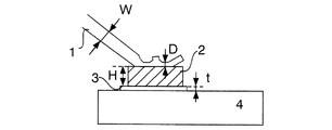
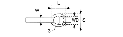
【解決手段】 電極膜3上に金属バンプ2を形成し、そのバンプ2上に金合金ボンディングワイヤ1をウェッジ接合する場合はそのバンプ2の高さHを2t+2≦H≦6t+50(μm)とする。さらにバンプのワイヤ結線方向に対して垂直方向の長さS、平行方向の長さL、ワイヤ径Wの関係が1.3W≦S≦4W、1.5W≦L≦5Wである。適切な高さ、形状を有する金属バンプを介して接合することにより、従来のボール接合よりも狭ピッチ接合に優れ、しかも高い長期信頼性を有する、半導体装置を提供するものである。
【選択図】 図1

Description

本発明は、金ボンディングワイヤを用いて、半導体素子上の電極と外部端子とを電気的に接続する半導体装置に関する。
現在半導体素子上の電極と外部リードとの間を接合するボンディングワイヤとしては、線径20〜50μm程度の金ボンディングワイヤが主として使用されている。金合金細線の接合技術としては超音波併用熱圧着方式が一般的である。金細線先端をアーク入熱で加熱溶融し、表面張力によりボールを形成させた後に、150〜300℃の範囲内で加熱した半導体素子の電極上にこのボール部を圧着接合せしめた後に、さらに外部リード側との接続を超音波圧着する方法である。トランジスタやIC等の半導体素子として使用するためには、前記の金合金細線によるボンディングの後に、Siチップ、ボンディングワイヤ、及びSiチップが取り付けられた部分のリードフレームを、これらを保護する目的で熱樹脂封止する。
半導体素子上の電極膜に用いられる材質は、現在、Al又はAl合金が主流である。最近、半導体素子の高集積化が進むに従い、Cu又はCu合金の電極膜が使用されて始めており、またCuの酸化防止等を目的として、表面にAl層又はAu層が形成されたCu又はCu合金の電極膜も実用化されている。
半導体素子の高集積化、高密度化の傾向により、金ボンディングワイヤの狭ピッチ接合が必要となっており、近年、金ボンディングワイヤの高強度細線化、狭ピッチ接合技術等が進歩してきている。しかし、狭ピッチ化が進むに従い、隣接するボール接合部の接触、あるいはキャピラリ冶具の先端形状の加工限界等の制約が問題となる。
従来のボール接合よりも狭ピッチに好適な接合として、ボール部を介さないで直接ワイヤを電極に接合するウェッジ接合がある。この接合では、ボールを形成しないため熱影響部がなくループ曲がりが低く抑えられる等、狭ピッチ接合の点で有利となる。しかし、ウェッジ接合法では超音波印加の方向性の制約等により、生産性が低下すること等の問題があり、金ワイヤによるウェッジ接合はほとんど実用化されておらず、現在でも金ワイヤではボール接合が主流である。
アルミ合金細線によるウェッジ接合は、セラッミックスパッケージされる半導体素子に利用されている。アルミ合金細線では、半導体素子上のアルミ電極との接合部において同種金属の接合により、高信頼性が得られる利点がある。しかし、アルミ合金細線を樹脂封止する半導体素子に使用すると、外部から侵入した水分等によりアルミ合金細線が腐食することが問題となるので、アルミ合金細線は樹脂封止パッケージへの適用は困難である。従って、アルミ合金細線の用途は限定され、しかも線径は100〜500μm程度の太径で使用される場合がほとんどである。
従来のウェッジ接合は、ボール接合に比して生産性が低いことが問題とされてきたが、ボンディング装置の性能向上等により、ウェッジ接合でもボール接合に匹敵する生産性が期待される。
今後、半導体実装の主流である樹脂封止パッケージにおいて、狭ピッチ化に適した、金合金細線をウェッジ接合する半導体装置が所望されている。
特開平9−275119号公報
金ワイヤのウェッジ接合法は、接続材料が金とアルミである点に関しては金ワイヤのボール接合法と類似しており、また、ワイヤを電極上に直接接合する点では、アルミ合金細線のウェッジ接合法と類似する。しかしながら、従来のボール接合技術及びアルミ合金細線の接合技術を用いただけでは、金ワイヤのウェッジ接合において接合性及び信頼性を確保することは困難であり、具体的な問題について下述する。
ウェッジ接合ではワイヤを直接接合するため、ワイヤ径の1.4〜2.5倍のボール部を接合するボール接合法と比べて接合面積が減少すること等の理由から、ボール接合の場合のような良好な金属接合を得ることが難しい。金合金細線のウェッジ接合でも、荷重を高めれば接合強度を増加することはできるものの、ワイヤも過剰に変形させてしまうため、ワイヤ断面積の減少及び過大な加工に伴ないワイヤ強度を著しく低下させることが問題となる。特に、接合部近傍の最弱部では、ループ形成時あるいは使用時にワイヤ破断に至る不良が発生してしまう。一方、アルミ合金細線によるウェッジ接合では、こうした接合部近傍での破断はほとんど問題とならない。その理由として、アルミ/アルミの同種金属接合のため接合強度が得易いこと、また現行のアルミ合金細線は金ワイヤの数十倍の太径であるため金ワイヤと比較して変形挙動が異なること等が挙げられる。つまり、太径のアルミ合金細線では、ワイヤ断面積の減少も非常に少ないため、接合部近傍でのワイヤ強度も十分確保することができる。
しかしながら、金ワイヤのウェッジ接合では狭ピッチ接合への対応が求められており、荷重、超音波振動等の接合条件だけの改善では、高速ボンディング時の量産性を高め、接合強度を確保することが困難である。一方、金ワイヤの変形量を減らすと、接合強度の低下をもたらす。これは、従来のボール接合に比べてウェッジ接合では、接合面積を高めるのが困難であり、破断を起こさないための変形許容量に制限がある等の要因が関連している。先述したように、こうした問題はアルミ合金細線では問題とならず、金ワイヤのウェッジ接合に特有の問題と考えられる。金ワイヤのウェッジ接合では、ワイヤ破断を起こさないで、しかも接合強度を確保することが課題となる。
また、半導体装置の高周波化により動作時の発熱量が増大し、また半導体の使用環境は自動車のエンジン周辺等のように高温に曝されること等から、接合部の長期信頼性に関する要求が高まっている。金ボール部と電極膜の接合部では、長期信頼性は良好であった。しかしながら、金ワイヤと電極膜とのウェッジ接合部では、長時間加熱されると接合強度が低下することが問題となる。この高温加熱における接合強度の低下は、接合不良の原因であり、金ワイヤのウェッジ接合の実用化を制約する一因となっていた。
こうしたAuワイヤのウェッジ接合に関する問題は、アルミ電極膜に限られたことでなく、電極材質がCu又はCu合金、またAl層又はAu層を上層とするCu又はCu合金の電極膜の場合にも、Auワイヤをウェッジ接合した場合に接合性及び長期信頼性が低下する問題が懸念されている。
本発明は、金ワイヤと電極膜とのウェッジ接合部において、接合性及び長期信頼性に優れた半導体装置を提供することを目的とする。
本発明者等は前述した観点から、金ワイヤと電極膜とのウェッジ接合部における接合性及び長期信頼性の支配要因について調査した結果、金属バンプを介して金ワイヤと電極膜を接合させ、しかもその金属バンプの厚さ、寸法、硬さが接合性及び長期信頼性に密接に関係していることを見出した。
すなわち、本発明は以下の構成を要旨とする。
(1) 半導体素子上のアルミ及びアルミ合金、Cu及びCu合金、Al層又はAu層を上層とするCu又はCu合金の膜厚tの電極膜上に、金属バンプあるいは、Au層またはAu合金層を表面に形成された金属バンプが形成され、該バンプが高純度Au、Au合金、Pt、Pd、Cu、これらの合金であり、そのバンプ上に金合金ボンディングワイヤがウェッジ接合されており、そのバンプ高さHが2t+2≦H≦6t+50(μm)であることを特徴とする半導体装置。
(2) さらにバンプのワイヤ結線方向に対して垂直方向の長さS、平行方向の長さL、ワイヤ径Wの関係が1.3W≦S≦4W、1.5W≦L≦5Wであることを特徴とする上記(1)に記載の半導体装置。
(3) バンプのビッカース硬度Hbとワイヤのビッカース硬度Hwの関係がHw−10≦Hb≦2Hwであることを特徴とする上記(1)に記載の半導体装置。
(4) さらにチップ面と平行な断面でみたバンプ内の結晶粒の平均径Gとワイヤ径Wの関係が、0.05W≦G≦0.7Wの範囲であることを特徴とする上記(1)に記載の半導体装置。
(5) 半導体素子上のアルミ及びアルミ合金、Cu及びCu合金、Al層又はAu層を上層とするCu又はCu合金の膜厚tの電極膜上に、高純度Au、Au合金、Pt、Pd、Cu、これらの合金の金属バンプが形成され、そのバンプ上に金合金ボンディングワイヤがウェッジ接合されており、且つそのバンプ高さHが2t+2≦H≦6t+50(μm)であり、さらにバンプのワイヤ結線方向に対して垂直方向の長さS、平行方向の長さL、ワイヤ径Wの関係が1.3W≦S≦4W、1.5W≦L≦5Wであり、さらにバンプのビッカース硬度Hbとワイヤのビッカース硬度Hwの関係がHw−10≦Hb≦2Hwの範囲であることを特徴とする半導体装置。
(6) 上記(1)〜(5)のいずれかに記載の半導体装置に用いる金合金ボンディングワイヤであって、引張破断強度F(MPa)が80〜400MPaで、破断伸びC(%)が1〜9%であり、さらに強度Fと伸びCの関係が150≦F・C≦2500の範囲であり、純度が99質量%以上の金であることを特徴とする半導体用の金合金ボンディングワイヤ。
本発明においては、金ワイヤと電極膜とのウェッジ接合部において、適切な高さ、形状を有する金属バンプを介して接合することにより、従来のボール接合よりも狭ピッチ接合に優れ、しかも高い長期信頼性を有する、半導体装置を提供するものである。
以下に、本発明に係わる半導体装置及びワイヤ等の構成についてさらに説明する。
本発明者らは、金ワイヤを電極上に接合すると言う点ではボール接合法とウェッジ接合法は類似しているものの、接合プロセス、キャピラリ冶具、接合部形態、寸法等の相違により、両者は接合性、長期信頼性が異なることを明らかにした。先述したように、金ワイヤのウェッジ接合法では、ボール接合に比べて長期信頼性及び接合性が低下することが問題であり、本発明者らは鋭意研究した結果、長期信頼性及び接合性を向上させるためのワイヤ、電極膜、バンプ等、各部位の構造(形態、厚さ、寸法、硬さ)について初めて見出した。具体的な接合構造と長期信頼性及び接合性との関係について下述する。
金ワイヤとアルミ電極膜との接合部が高温に曝されると、接合界面ではAu−Al化合物相が成長し、この化合物相の成長が接合性及び長期信頼性と関連しており、従来のAuワイヤのボール接合では、良好な接合性及び長期信頼性を比較的容易に確保できることが知られていた。本発明者らはウェッジ接合部の拡散挙動を詳細に調査した結果、ボール接合とウェッジ接合では、Auの厚み等の供給量の差異により、化合物相の成長挙動が異なることを見出した。
金ボールを用いた接合部では、金ボール部の厚さはアルミ電極膜厚よりも十分厚いため、拡散が進行して接合部直下のアルミ電極膜中におけるAl層が消失する。その後も、金ボール部にはAuが十分に存在しているのでAu原子の供給が継続されるため、化合物相はよりAu−richな相(主にAu4Al相)へと変化する。
それに比して、ウェッジ接合では、ワイヤの圧着厚さがボール接合と比して小さいため、原子の拡散が十分進行すると、接合部でのアルミ電極のAlと金ワイヤ部のAuともに拡散に消費されてしまう。その後はAu原子が供給されなくなるため、ウェッジ接合部で成長する化合物相は、ボール接合の場合と比べてAl−richな相(例えばAu2Al、AuAl2相)となる。こうしたボール接合とは異なる化合物相が成長することが、ウェッジ接合において長期信頼性を低下させている原因であることを明らかにした。
Auバンプ又はAu合金バンプを介して金ワイヤと電極膜を接合することにより、電極膜に対する相対的な金の厚さを十分確保することができ、さらに、良好な接合性も得られる。図1に、金属バンプ2を介してウェッジ接合した部位を水平側から見た図を示す。但し、バンプ形成しただけでは長期信頼性を低下させる場合があることから、バンプを介したウェッジ接合において長期信頼性を確保するためにはバンプ高さの制御が重要であり、バンプ高さと電極膜厚との関係をある範囲に制御することにより、高温での長期信頼性を高められることを見出した。すなわち、そのバンプ高さHと電極厚tの関係が、2t+2≦H≦6t+50(μm)の範囲であれば、電極膜に対する相対的な金の厚さを十分確保し、良好な接合性も得られるが、バンプ高さH(μm)が2t+2(μm)よりも低ければ、バンプによる接合強度を高める効果は得られず、一方、バンプ高さH(μm)が6t+50(μm)よりも厚ければ、バンプ変形に伴ないワイヤの直線性が低下するため、狭ピッチでは隣接するワイヤが接触する問題が発生してしまう。
さらに、金ワイヤとバンプとの接合部における接合性及び長期信頼性を確保することも重要であり、金ワイヤの線径とバンプ高さとの間にも満足すべき関係があることを見出した。つまり、使用するワイヤ径Wとバンプ高さHの関係が、1.7t+0.2W−2≦H≦4.5t+1.5W+10(μm)の範囲であれば、ワイヤ径が10〜30μmの範囲において、長期信頼性を確保するためのバンプ高さを維持することができ、接合強度も高くすることができる。この理由として、接合性を高めるためにワイヤの変形量を十分高めた場合にも、1.7t+0.2W−2≦H(μm)であれば、ワイヤ接合部の直下に必要なバンプ高さを十分確保することができるためである。また、バンプ高さHが高過ぎると接合時の荷重によりバンプ形状が崩れて、狭ピッチの場合に隣接バンプが接触することが懸念されるが、H≦4.5t+1.5W+10(μm)であれば、線径に関係なく、接合後にも良好なバンプ形状を維持できるためである。
金ワイヤを金バンプ上に接合する際に良好な接合性を確保するためには、バンプの長さも重要な因子である。図2及び図3に、チップに垂直側から見たウェッジ接合部位を示す。ウェッジ接合されたワイヤの結線方向に対して垂直及び平行方向におけるバンプ長さをそれぞれS、Lとすると、1.3W≦S≦4W、1.5W≦L≦5Wの範囲にすれば、接合面積を十分高めて良好な接合性が得られる。これは、接合強度を高めるためには接合されたワイヤの圧着幅WDを高めることが重要で、このワイヤ圧着幅WDが線径Wの1.2〜3.0倍であれば接合性が良好であり、また汎用ワイヤボンディング装置の位置精度等を考慮すれば、上記範囲を満足することにより、接合強度を高めて、良好な接合性が得られると言う理由に基づく。すなわち、ワイヤ結線と垂直方向のバンプ幅S、平行方向のバンプ長Lについて、1.3W≦S、1.5W≦Lであれば、ワイヤがバンプよりはみ出すことを抑え、接合強度を高め、そのばらつきを低減することができ、またS≦4W、L≦5Wの大きさのバンプであれば、隣接する接合部間隔も小さくでき、狭ピッチ化に十分対応できるためである。今後の狭ピッチ化、低温接合、に適応するために接合強度をさらに向上し、あるいは高速接合等により生産性を向上するためには、上記のバンプ形状において、1.6W≦S≦3W、1.7W≦L≦4Wの範囲であることがより好ましい。
さらに、ウェッジ接合において、接合強度の増加、狭ピッチ対応のキャピラリの加工限界等まで含めて考慮すると、ワイヤ結線方向の長さLの方が垂直方向の長さSよりも長くして、その関係が1.2S+5≦L≦2S+20(μm)の範囲であることが、より好ましい。
バンプの形状は角形、球形、円柱形等いずれでも可能である。そのバンプの形成法は、ワイヤを用いたスタッドバンプ法、微細球によるボールバンプ、メッキ形成等のいずれでも接合性及び長期信頼性を高めることができる。但し、これらの手法では生産性、操作法、必要設備等には差があり、スタッドバンプ法ではウェッジ接合用のワイヤでバンプ形成できるため、工程が簡便であるものの、バンプ形状のバラツキが大きいことが懸念される。また、メッキで形成したバンプでは、メッキ設備が必要であり、厚いバンプを形成するには時間を要するものの、角形、円柱形等の目的とするバンプ形状の作製が容易であり、高さのバラツキをスタッドバンプ法より低減することが可能である。一方、ボールバンプを利用すれば、予め作製したボールを電極上に配列し、さらに電極上に接合する工程は要するものの、ボールの寸法、成分等を変更することにより、目的に合わせたバンプの材質を容易に得られる。
バンプ素材は、高純度Au又はAu合金であることが望ましいが、Pt、Pd、Cu又はそれらの合金であっても、本願の目的とする機能が得られることを確認した。
さらに、Pt、Pd、Cu又はそれらの合金のバンプの上部に、Au層又はAu合金層が形成されたバンプを用い、ワイヤ、電極膜、バンプ等の厚さ、寸法等を上述した関係を満足するウェッジ接合により、接合性、作業性等をより高めることができる。すなわち、これらのバンプと金ワイヤとのウェッジ接合部では、バンプ表面の酸化を抑えられ、しかもAu/Au接合を得ることにより、接合強度をより高めることができる。バンプ上部のAu層又はAu合金層の厚さは、0.01〜2μmの厚みであれば十分な効果が得られ、その表面層の形成ではスパッタ法又はメッキ法等が可能である。
金バンプ上への金ワイヤの接合強度を高めるためには、ワイヤ及びバンプの硬さも重要であり、ある関係を満足するとより好ましいことを確認した。つまり、バンプのビッカース硬度Hbとワイヤのビッカース硬度HwはHw−10≦Hb≦2Hwの関係を満足すれば、ウェッジ接合時にワイヤとバンプ共に適度に変形するため十分な接合性が得られ、ワイヤの直線性も確保することができる。一方、Hb<Hw+10であれば、軟らかいバンプが優先的に変形するため、隣接するバンプが接触したり、ワイヤの直線性が低下したりして、60μm以下の狭ピッチ化への対応が困難であり、一方、Hb>2Hwであれば、ワイヤの変形がほとんどであり、最も変形した部位でのワイヤの引張強度が低下するため、この部位で破断に到る不良が発生してしまう。さらに、硬度の関係がHw−5≦Hb≦1.6Hwであることがより望ましく、これは、Hw−5≦Hbであれば、キャピラリ先端への金バンプの付着を抑制して、キャピラリの交換寿命を上昇させることができ、またHb≦1.6Hwであればワイヤとバンプが均等に変形して接合強度のばらつきが低減すると言う理由に基づく。
バンプ組織もバンプの変形挙動に影響を及ぼしており、チップ面と平行なバンプ断面での結晶粒の平均径Gとワイヤ径Wの関係が、0.05W≦G≦0.7Wの範囲であることが好ましい。これは、0.05W≦Gであればバンプ変形の異方性を低減して狭ピッチに対応でき、またG>0.7Wであれば、ある方向へのバンプ変形が著しくなり、隣接するワイヤが接触するためである。
ウェッジ接合における接合性、接合信頼性を向上するために、ワイヤ、電極材、金属バンプの厚さ、硬度、寸法等について、本発明に係わる関係を実現する手段として、特に、ワイヤの機械的特性、表面性状を調整することが有効であることを見出した。電極材、金属バンプ等の材質を変更すると、配線工程、電気的性能等も影響を受けるため、それらを評価し、適正化することまで検討しなくてはならない場合が多いのに対して、ワイヤの材質の変更は比較的容易であり、しかも接合性、接合信頼性を向上する効果も大きい。
すなわち、引張破断強度F(MPa)が80〜400MPaで、破断伸びC(%)が1〜9%であり、さらに強度Fと伸びCの関係が150≦F・C≦2500の範囲であり、純度が99質量%の金である金合金ワイヤを用いると、良好なウェッジ接合が得られる。
ワイヤの引張破断強度F(MPa)と破断伸びC(%)との積が一定の関係を満足することにより、ウェッジ接合における接合性、接合信頼性を高めることができ、その強度Fと伸びCの関係としては、150≦F・C≦2500の範囲であることが望ましいことを見出した。これは、F・C<150であれば、ウェッジ接合時にワイヤが過剰に変形して、接合信頼性が低下することが問題であり、F・C>2500であれば、ワイヤが接合強度を高めることが困難なためである。
さらに、ウェッジ接合性だけでなく、ワイヤのループ形成、樹脂封止時のワイヤ変形等の要求特性を十分満足するためには、F・Cの積を上記の範囲とすることに加えて、引張破断強度Fが80〜400MPaであり、破断伸びCが1〜9%の範囲であることが必要である。これは、強度Fが80MPa未満であれば、ループが下方に垂れる問題が発生し、Fが400MPaを超えるとウェッジ接合時にチップに損傷を与えたり、ループ形状を制御することが困難となり、ループ高さのバラツキが大きくなることが問題となるためである。また、破断伸びCが1%未満であれば、ウェッジ接合部での強度を確保すること困難であり、Cが9%を超えると、ループ形成されたワイヤの直線性が低下することが問題である。
ワイヤの素材は純度99%以上を有する金合金ワイヤである。つまり、本発明での金合金ワイヤとは、純度1%以下の添加元素を含有するワイヤ及び、純度が99.99%以上であり、残りを不可避不純物とする高純度金ワイヤも含まれる。例えば、Ca、Be、Cu、Ag、Pt、Pd等から1種類以上の元素を総計で0.0001〜1%の範囲で含有し、残部がAuであり、それをダイス伸線により20〜30μmに伸線した金合金ワイヤを用いれば、良好なウェッジ接合特性が得られる。
また、ワイヤを金属バンプに直接接続するウェッジ接合では、上述した、ワイヤの機械的特性に加えて、ワイヤの表面性状も重要であり、ワイヤ表面から10nmの深さまでの平均酸素濃度が10at%以下であることが、ウェッジ接合性の向上には有効であることを見出した。これは、10nmの深さまでの平均酸素濃度が10at%を超えると、接合時に接合強度を低下させる原因となり、また、その酸素濃度が高い表層部を破壊させて良好な接合を得るには、超音波振動を高める必要があり、これに伴い、チップへの損傷、ワイヤの直線性の低下等の問題が発生するためである。ワイヤ表面の平均酸素濃度は、例えばオージェ分光法にて測定できる。
以上のことから、ワイヤの引張破断強度F(MPa)が80〜400MPaで、破断伸びC(%)が1〜9%であり、さらに強度Fと伸びCの関係が150≦F・C≦2500の範囲であり、ワイヤ表面から10nmの深さまでの平均酸素濃度が10at%以下とすることにより、ウェッジ接合部の接合性、接合信頼性を向上することができ、さらに良好なループ形状が得られ、樹脂封止時のワイヤ変形も抑制することができ、狭ピッチ接合に適応できることを確認した。こうした性能を有する金ワイヤを得るためには、金中の元素添加、あるいはワイヤ伸線加工技術及び熱処理条件の適正化等が有効であることを確認した。
金ワイヤを電極上にウェッジ接合する手法としては、これまで中心的に述べた、ボール部を形成しないで接続するウェッジ−ウェッジ接合法の他に、電極側にボール部を接合する通常のボール接合とは異なり、ワイヤを電極側にウェッジ接合する方法や、チップ同士の電極間をボール−ウェッジ接合する方法もある。こうした電極側にワイヤをウェッジ接合することは、接合面積を縮小できるため狭ピッチ接続には有利であり、また、複数のチップを接続する場合にも活用できる。前述した、ウェッジ接合における接合性及び信頼性の低下は、電極側にワイヤをウェッジ接合する手法に共通する問題である。従って、本発明に係わる半導体装置及び、それに用いられる金合金ワイヤは、電極側にワイヤをウェッジ接合する方法であれば、ウェッジ−ウェッジ接合、ボール−ウェッジ接合の両手法に適用されるものである。
以下、実施例について説明する。ワイヤには、高純度金ワイヤ(純度>99.99%)又は、Ca、Be、Cu、Ag、Pt、Pd等から1種類以上の元素を総計で0.0001〜1%の範囲で含有する金合金ワイヤを用い、その線径Wは15〜30μmとした。ワイヤの強度又は硬度を調整するために、ワイヤ製造工程において、伸線ダイス減面率(2〜15%)、伸線速度(10〜600m/min)及び、最終段階での熱処理温度(200〜700℃)等を選定した。シリコン基板上の電極材質には、純Al、Al合金(Al−1%Si、Al−0.5%Cu)、純Cu、またAl層又はAu層を上層(0.1μm)とする純Cu膜等を使用し、電極膜の厚さtは0.5〜4μmとした。市販の自動ウェッジボンダーを使用して、電極上にワイヤを接合した。
電極上への金バンプの形成は、スタッドバンプ法、ボールバンプ法、メッキ法等を使用し、さらに金バンプ上に、上述した方法で金ワイヤをウェッジ接合した。スタッドバンプ法では、25μm径の金ワイヤの先端を溶融生成したボール部(ボール径:35〜60μm)を電極に接合し、その平板冶具で荷重を付加してバンプ高さを調整した。また、ボールバンプ法では、純度2N(>99%)の金で球径30〜60μmの球を作製し、手動の配列装置を用いて、約100個の金ボールを電極上に一括接合した。メッキ法では、メッキ浴中にシリコン基板を浸漬して電解メッキにより、Au、Pt、Pd、Cu等の素材からなるバンプを電極膜上に形成した。
ワイヤの引張破断強度及び伸び率は、長さ10cmのワイヤ5本の引張試験を実施し、その平均値により求めた。ワイヤ及びバンプの硬度測定は、ビッカース硬度測定法に基づいて、29mNの荷重で測定し、5点の平均値を求めた。ワイヤ表面の酸素濃度の測定は、オージェ分光装置を用い、ワイヤ表面をスパッタしながら、10nmの深さの平均値を求めた。
ワイヤ接合部の強度評価としては、プル試験法を用いた。このプル試験法は、ボンディングワイヤ後にリードフレームと測定する半導体素子を固定した状態で、ボンディング後の金合金細線をフックで上方に引張り、そのときの破断強度を40本測定し、プル強度の平均値及び標準偏差を評価した。その際、電極との接合性を評価するために、フックを掛けて上方引張する箇所を、中央部よりも電極に近いところで試験した。
長期信頼性の評価として、金ワイヤを電極にウェッジ接合した半導体装置を樹脂封止しない状態で、窒素ガス中において185℃で300時間加熱した後に、40本のプル強度を測定した。金ワイヤのウェッジ接合した半導体装置が用いられる使用温度での寿命評価として、185℃300時間の加熱試験は十分と考えられ、この加熱により強度が低下しない場合には、接合部の長期信頼性は良好であると判断できる。
金合金細線のループ形成時のワイヤ曲がりは、ワイヤ長さが約5mmとなるようボンディングを行った後に、半導体素子とほぼ垂直上方向からワイヤを投影機を用いて観察し、ワイヤ中心部からワイヤの両端接合部を結ぶ直線と、ワイヤの曲がりが最大の部分との垂線の距離を50本測定した平均値で示した。
接合時のチップ損傷を調べるため、ボンディングした素子を王水中に数分間つけて、金ワイヤ及び電極等を溶解した後に、200個の接合箇所を光学顕微鏡及びSEMで観察した。光顕観察でもクラックが観察された場合は損傷が大きいとして×印、光顕では損傷は観察されないが、2000倍程度の倍率で微小な傷又は穴が認められるものは○印、光顕及びSEM観察において損傷が認められない場合は◎印で示した。
バンプ内の断面組織を観察するため、チップ面と平行に断面研磨を行い、エッチングした後で、バンプ内の結晶粒の数を測定し、1個のバンプ断面での粒径を計算した。さらに、それを20個のバンプで測定して、バンプ内の結晶粒の平均粒径を求めた。
Figure 2005294874
Figure 2005294874
表1において、金バンプを用いた接合に関して、実施例1〜28ではバンプ高さと電極膜厚の関係を第1の発明である2t+2≦H≦6t+50(μm)の条件範囲とし、実施例1〜16及び21〜28では、上記厚さの関係に加えて、ワイヤ径とバンプ寸法の関係を第2の発明である1.3W≦S≦4W、1.5W≦L≦5Wの条件範囲とし、実施例1〜24は、上記厚さの関係に加えて、ワイヤとバンプの硬さの関係を第3の発明であるHw−10≦Hb≦2Hwの条件範囲に調整したもので、中でも、本発明例9、13、23、24では、バンプ表面にAu層を形成するものに関する。また、実施例1〜20及び23〜28は、第4の発明であるバンプ内の結晶粒径の関係を0.05W≦G≦0.7Wの条件範囲に調整したものである。
また表2の比較例1〜4は、金バンプを介して接合しているが、そのバンプ高さの関係が第1の発明に該当しない例について、それぞれ比較として示した。
本発明例1〜28は、金ワイヤと電極膜の間に金属バンプを介してウェッジ接合しており、しかもそのバンプ高さHと電極厚tの関係は2t+2≦H≦6t+50(μm)の範囲であることから、接合性及び長期信頼性は非常に良好であった。Auバンプの形成法で比較すると、スタッドバンプ法、ボールバンプ法、メッキ法のいずれの方法で形成した場合も、同様の結果が得られた。一方、比較例1、3は、バンプを介して接合されているが、2t+2>H(μm)であるため、加熱後のプル強度は低下しており、パンプは一定高さ以上が必要であることが確認された。
バンプ素材がPt、Pd、Cu等の場合も、十分な接合性、接合信頼性が得られていた。第2の発明に関する本発明例9、13、23、24では、バンプ表面にAu層を0.1μm程度形成することにより、高い接合強度が得られており、例えば本発明例13では、ワイヤ単位面積当りのプル強度が、Cuバンプでは上層部が形成されていない本発明例12よりも15MPaも増加することが確認された。
バンプの寸法とワイヤ径Wの関係を比較すると、本発明例17、19は1.3W>Sであり、本発明例18、20は1.5W>Lとなるため、接合直後のプル強度のばらつきが若干大きいのに比べて、本発明例9〜16では、ワイヤ径及びバンプ寸法の絶対値は異なっていても、第2の発明に係わる、1.3W≦S≦4W、1.5W≦L≦5Wの条件を満足するため、プル強度は高く、しかもその値のばらつきも小さく抑えられていることが確認された。
バンプのビッカース硬度Hbとワイヤのビッカース硬度Hwを比較すると、Hb<Hw−10である本発明例25、26では、バンプ上にウェッジ接合したワイヤの曲がり量が比較的大きく、またHb>2Hwである本発明例27、28では、ワイヤ単位面積当りのプル強度の上昇効果は若干低い結果が得られた。それに比して、第3の発明の範囲を満足している本発明例1〜24では、バンプとワイヤの硬度の関係がHw−10≦Hb≦2Hwの範囲におさまっており、接合性及び長期信頼性は優れていることが確認された。
バンプ断面での結晶粒径Gとワイヤ径Wの関係を比較すると、実施例1〜20及び23〜28では、第4の発明に係わる0.05W≦G≦0.7Wの関係を満足するため、プル強度は高く、ワイヤの曲がり量も小さく抑えられていた。それに対し、本発明例21、22では、それぞれG>0.7W、G<0.05Wとなり、ワイヤの曲がり量が比較的大きく、これは通常の接続では問題のないレベルであるが、狭ピッチ接続では懸念される。
本発明例1〜28では、ワイヤの特性をみれば第6の発明に係わる特性を有しており、具体的には、引張破断強度Fが80〜400MPaで、破断伸びCが1〜9%であり、さらに強度Fと伸びCの関係が150≦F・C≦2500の範囲であった。
電極上に形成した金属バンプの上への、金ワイヤのウェッジ接合部を水平方向から見た図である。 金ワイヤのウェッジ接合部を上方からみた図を示す。 金ワイヤのウェッジ接合部を上方からみた図を示す。
符号の説明
1:金合金ワイヤ
2:金属バンプ
3:電極膜
4:シリコン基板
W:ワイヤ径
D:ワイヤ圧着厚さの最小値
t:電極の膜厚
H:バンプ高さ
S:バンプの横長さ
L:バンプの縦長さ
WD:ウェッジ接合されたワイヤの圧着幅

Claims (6)

  1. 半導体素子上のアルミ及びアルミ合金、Cu及びCu合金、Al層又はAu層を上層とするCu又はCu合金の膜厚tの電極膜上に、金属バンプあるいは、Au層またはAu合金層を表面に形成された金属バンプが形成され、該バンプが高純度Au、Au合金、Pt、Pd、Cu、これらの合金であり、そのバンプ上に金合金ボンディングワイヤがウェッジ接合されており、そのバンプ高さHが2t+2≦H≦6t+50(μm)であることを特徴とする半導体装置。
  2. さらにバンプのワイヤ結線方向に対して垂直方向の長さS、平行方向の長さL、ワイヤ径Wの関係が1.3W≦S≦4W、1.5W≦L≦5Wであることを特徴とする請求項1に記載の半導体装置。
  3. バンプのビッカース硬度Hbとワイヤのビッカース硬度Hwの関係がHw−10≦Hb≦2Hwであることを特徴とする請求項1に記載の半導体装置。
  4. さらにチップ面と平行な断面でみたバンプ内の結晶粒の平均径Gとワイヤ径Wの関係が、0.05W≦G≦0.7Wの範囲であることを特徴とする請求項1に記載の半導体装置。
  5. 半導体素子上のアルミ及びアルミ合金、Cu及びCu合金、Al層又はAu層を上層とするCu又はCu合金の膜厚tの電極膜上に、高純度Au、Au合金、Pt、Pd、Cu、これらの合金の金属バンプが形成され、そのバンプ上に金合金ボンディングワイヤがウェッジ接合されており、且つそのバンプ高さHが2t+2≦H≦6t+50(μm)であり、さらにバンプのワイヤ結線方向に対して垂直方向の長さS、平行方向の長さL、ワイヤ径Wの関係が1.3W≦S≦4W、1.5W≦L≦5Wであり、さらにバンプのビッカース硬度Hbとワイヤのビッカース硬度Hwの関係がHw−10≦Hb≦2Hwの範囲であることを特徴とする半導体装置。
  6. 請求項1〜5のいずれかに記載の半導体装置に用いる金合金ボンディングワイヤであって、引張破断強度F(MPa)が80〜400MPaで、破断伸びC(%)が1〜9%であり、さらに強度Fと伸びCの関係が150≦F・C≦2500の範囲であり、純度が99質量%以上の金であることを特徴とする半導体用の金合金ボンディングワイヤ。
JP2005197314A 2005-07-06 2005-07-06 ワイヤをウェッジ接合した半導体装置及び金合金ボンディングワイヤ Pending JP2005294874A (ja)

Priority Applications (1)

Application Number Priority Date Filing Date Title
JP2005197314A JP2005294874A (ja) 2005-07-06 2005-07-06 ワイヤをウェッジ接合した半導体装置及び金合金ボンディングワイヤ

Applications Claiming Priority (1)

Application Number Priority Date Filing Date Title
JP2005197314A JP2005294874A (ja) 2005-07-06 2005-07-06 ワイヤをウェッジ接合した半導体装置及び金合金ボンディングワイヤ

Related Parent Applications (1)

Application Number Title Priority Date Filing Date
JP2000120333A Division JP3764629B2 (ja) 2000-04-21 2000-04-21 ワイヤをウェッジ接合した半導体装置

Publications (1)

Publication Number Publication Date
JP2005294874A true JP2005294874A (ja) 2005-10-20

Family

ID=35327382

Family Applications (1)

Application Number Title Priority Date Filing Date
JP2005197314A Pending JP2005294874A (ja) 2005-07-06 2005-07-06 ワイヤをウェッジ接合した半導体装置及び金合金ボンディングワイヤ

Country Status (1)

Country Link
JP (1) JP2005294874A (ja)

Cited By (4)

* Cited by examiner, † Cited by third party
Publication number Priority date Publication date Assignee Title
JP2009302261A (ja) * 2008-06-12 2009-12-24 Toyota Central R&D Labs Inc 半導体装置
JP2010123817A (ja) * 2008-11-21 2010-06-03 Fujitsu Ltd ワイヤボンディング方法および電子装置とその製造方法
JP2010157683A (ja) * 2008-12-03 2010-07-15 Renesas Technology Corp 半導体集積回路装置
US8174104B2 (en) * 2008-06-09 2012-05-08 Micronas Gmbh Semiconductor arrangement having specially fashioned bond wires

Citations (3)

* Cited by examiner, † Cited by third party
Publication number Priority date Publication date Assignee Title
JPH02114545A (ja) * 1988-10-24 1990-04-26 Toshiba Corp ワイヤボンディング接続方法
JPH09275119A (ja) * 1996-04-04 1997-10-21 Nippon Steel Corp 半導体装置
JPH10512399A (ja) * 1995-09-26 1998-11-24 シーメンス アクチエンゲゼルシヤフト 半導体チップを少なくとも1つの接触面と電気的に接続する方法

Patent Citations (3)

* Cited by examiner, † Cited by third party
Publication number Priority date Publication date Assignee Title
JPH02114545A (ja) * 1988-10-24 1990-04-26 Toshiba Corp ワイヤボンディング接続方法
JPH10512399A (ja) * 1995-09-26 1998-11-24 シーメンス アクチエンゲゼルシヤフト 半導体チップを少なくとも1つの接触面と電気的に接続する方法
JPH09275119A (ja) * 1996-04-04 1997-10-21 Nippon Steel Corp 半導体装置

Cited By (4)

* Cited by examiner, † Cited by third party
Publication number Priority date Publication date Assignee Title
US8174104B2 (en) * 2008-06-09 2012-05-08 Micronas Gmbh Semiconductor arrangement having specially fashioned bond wires
JP2009302261A (ja) * 2008-06-12 2009-12-24 Toyota Central R&D Labs Inc 半導体装置
JP2010123817A (ja) * 2008-11-21 2010-06-03 Fujitsu Ltd ワイヤボンディング方法および電子装置とその製造方法
JP2010157683A (ja) * 2008-12-03 2010-07-15 Renesas Technology Corp 半導体集積回路装置

Similar Documents

Publication Publication Date Title
JP5550369B2 (ja) 半導体用銅ボンディングワイヤとその接合構造
JP4866490B2 (ja) 半導体用銅合金ボンディングワイヤ
WO2012169067A1 (ja) 高強度、高伸び率金合金ボンディングワイヤ
CN100557784C (zh) 接合引线用金合金线
JP5343069B2 (ja) ボンディングワイヤの接合構造
JP4705078B2 (ja) 半導体装置用銅合金ボンディングワイヤ
JP2010245390A (ja) ボンディングワイヤ
JP2005268771A (ja) 半導体装置用金ボンディングワイヤ及びその接続方法
JP2005294874A (ja) ワイヤをウェッジ接合した半導体装置及び金合金ボンディングワイヤ
WO2006134825A1 (ja) 高い初期接合性、高い接合信頼性、圧着ボールの高い真円性、高い直進性、高い耐樹脂流れ性および低い比抵抗を有するボンディングワイヤ用金合金線
JP3650461B2 (ja) 半導体素子用金合金細線
JP3764629B2 (ja) ワイヤをウェッジ接合した半導体装置
JP3445616B2 (ja) 半導体素子用金合金細線
JP4947670B2 (ja) 半導体素子用ボンディングワイヤの熱処理方法
JP3426473B2 (ja) 半導体素子用金合金細線
JP3593206B2 (ja) バンプ用金合金細線および金合金バンプ
JP4134261B1 (ja) ボールボンディング用金合金線
JP3426397B2 (ja) 半導体素子用金合金細線
JP3747023B2 (ja) 半導体用金ボンディングワイヤ
JP2003133362A (ja) 半導体装置及び半導体装置用ボンディングワイヤ
JP3571793B2 (ja) 金合金細線および金合金バンプ
TW202234482A (zh) 半導體裝置用Ag合金接合線
JPH08293516A (ja) 半導体素子用金合金細線
JPH08293514A (ja) 半導体素子用金合金細線
JPH09198917A (ja) 半導体素子用金合金細線

Legal Events

Date Code Title Description
A621 Written request for application examination

Free format text: JAPANESE INTERMEDIATE CODE: A621

Effective date: 20060217

A711 Notification of change in applicant

Free format text: JAPANESE INTERMEDIATE CODE: A712

Effective date: 20061019

RD03 Notification of appointment of power of attorney

Free format text: JAPANESE INTERMEDIATE CODE: A7423

Effective date: 20070124

A977 Report on retrieval

Free format text: JAPANESE INTERMEDIATE CODE: A971007

Effective date: 20080522

A131 Notification of reasons for refusal

Free format text: JAPANESE INTERMEDIATE CODE: A131

Effective date: 20080603

A521 Written amendment

Free format text: JAPANESE INTERMEDIATE CODE: A523

Effective date: 20080731

A131 Notification of reasons for refusal

Free format text: JAPANESE INTERMEDIATE CODE: A131

Effective date: 20100105

A02 Decision of refusal

Free format text: JAPANESE INTERMEDIATE CODE: A02

Effective date: 20100518