EP0847194A2 - Steuerung des Anzeigepegels in der Bildbrandbereiche einer Anzeigevorrichtung mit einer Flüssigkristallanzeigetafel - Google Patents
Steuerung des Anzeigepegels in der Bildbrandbereiche einer Anzeigevorrichtung mit einer Flüssigkristallanzeigetafel Download PDFInfo
- Publication number
- EP0847194A2 EP0847194A2 EP97121206A EP97121206A EP0847194A2 EP 0847194 A2 EP0847194 A2 EP 0847194A2 EP 97121206 A EP97121206 A EP 97121206A EP 97121206 A EP97121206 A EP 97121206A EP 0847194 A2 EP0847194 A2 EP 0847194A2
- Authority
- EP
- European Patent Office
- Prior art keywords
- picture elements
- display
- frame
- signals
- image
- Prior art date
- Legal status (The legal status is an assumption and is not a legal conclusion. Google has not performed a legal analysis and makes no representation as to the accuracy of the status listed.)
- Withdrawn
Links
- 239000004973 liquid crystal related substance Substances 0.000 title claims abstract description 34
- 239000011159 matrix material Substances 0.000 claims abstract description 7
- 238000012358 sourcing Methods 0.000 claims 1
- 238000010586 diagram Methods 0.000 description 7
- 238000000034 method Methods 0.000 description 3
- 230000000694 effects Effects 0.000 description 2
- 230000002093 peripheral effect Effects 0.000 description 2
- 239000003086 colorant Substances 0.000 description 1
- 238000010276 construction Methods 0.000 description 1
- 238000005516 engineering process Methods 0.000 description 1
- 230000000977 initiatory effect Effects 0.000 description 1
- 238000005070 sampling Methods 0.000 description 1
- 239000010409 thin film Substances 0.000 description 1
Images


Classifications
-
- G—PHYSICS
- G09—EDUCATION; CRYPTOGRAPHY; DISPLAY; ADVERTISING; SEALS
- G09G—ARRANGEMENTS OR CIRCUITS FOR CONTROL OF INDICATING DEVICES USING STATIC MEANS TO PRESENT VARIABLE INFORMATION
- G09G5/00—Control arrangements or circuits for visual indicators common to cathode-ray tube indicators and other visual indicators
- G09G5/003—Details of a display terminal, the details relating to the control arrangement of the display terminal and to the interfaces thereto
- G09G5/006—Details of the interface to the display terminal
- G09G5/008—Clock recovery
-
- G—PHYSICS
- G09—EDUCATION; CRYPTOGRAPHY; DISPLAY; ADVERTISING; SEALS
- G09G—ARRANGEMENTS OR CIRCUITS FOR CONTROL OF INDICATING DEVICES USING STATIC MEANS TO PRESENT VARIABLE INFORMATION
- G09G3/00—Control arrangements or circuits, of interest only in connection with visual indicators other than cathode-ray tubes
- G09G3/20—Control arrangements or circuits, of interest only in connection with visual indicators other than cathode-ray tubes for presentation of an assembly of a number of characters, e.g. a page, by composing the assembly by combination of individual elements arranged in a matrix no fixed position being assigned to or needed to be assigned to the individual characters or partial characters
- G09G3/34—Control arrangements or circuits, of interest only in connection with visual indicators other than cathode-ray tubes for presentation of an assembly of a number of characters, e.g. a page, by composing the assembly by combination of individual elements arranged in a matrix no fixed position being assigned to or needed to be assigned to the individual characters or partial characters by control of light from an independent source
- G09G3/36—Control arrangements or circuits, of interest only in connection with visual indicators other than cathode-ray tubes for presentation of an assembly of a number of characters, e.g. a page, by composing the assembly by combination of individual elements arranged in a matrix no fixed position being assigned to or needed to be assigned to the individual characters or partial characters by control of light from an independent source using liquid crystals
- G09G3/3611—Control of matrices with row and column drivers
- G09G3/3648—Control of matrices with row and column drivers using an active matrix
-
- G—PHYSICS
- G09—EDUCATION; CRYPTOGRAPHY; DISPLAY; ADVERTISING; SEALS
- G09G—ARRANGEMENTS OR CIRCUITS FOR CONTROL OF INDICATING DEVICES USING STATIC MEANS TO PRESENT VARIABLE INFORMATION
- G09G2300/00—Aspects of the constitution of display devices
- G09G2300/08—Active matrix structure, i.e. with use of active elements, inclusive of non-linear two terminal elements, in the pixels together with light emitting or modulating elements
- G09G2300/0809—Several active elements per pixel in active matrix panels
- G09G2300/0814—Several active elements per pixel in active matrix panels used for selection purposes, e.g. logical AND for partial update
-
- G—PHYSICS
- G09—EDUCATION; CRYPTOGRAPHY; DISPLAY; ADVERTISING; SEALS
- G09G—ARRANGEMENTS OR CIRCUITS FOR CONTROL OF INDICATING DEVICES USING STATIC MEANS TO PRESENT VARIABLE INFORMATION
- G09G2310/00—Command of the display device
- G09G2310/02—Addressing, scanning or driving the display screen or processing steps related thereto
- G09G2310/0232—Special driving of display border areas
-
- G—PHYSICS
- G09—EDUCATION; CRYPTOGRAPHY; DISPLAY; ADVERTISING; SEALS
- G09G—ARRANGEMENTS OR CIRCUITS FOR CONTROL OF INDICATING DEVICES USING STATIC MEANS TO PRESENT VARIABLE INFORMATION
- G09G2340/00—Aspects of display data processing
- G09G2340/04—Changes in size, position or resolution of an image
- G09G2340/0464—Positioning
- G09G2340/0471—Vertical positioning
-
- G—PHYSICS
- G09—EDUCATION; CRYPTOGRAPHY; DISPLAY; ADVERTISING; SEALS
- G09G—ARRANGEMENTS OR CIRCUITS FOR CONTROL OF INDICATING DEVICES USING STATIC MEANS TO PRESENT VARIABLE INFORMATION
- G09G2340/00—Aspects of display data processing
- G09G2340/04—Changes in size, position or resolution of an image
- G09G2340/0464—Positioning
- G09G2340/0478—Horizontal positioning
-
- G—PHYSICS
- G09—EDUCATION; CRYPTOGRAPHY; DISPLAY; ADVERTISING; SEALS
- G09G—ARRANGEMENTS OR CIRCUITS FOR CONTROL OF INDICATING DEVICES USING STATIC MEANS TO PRESENT VARIABLE INFORMATION
- G09G2340/00—Aspects of display data processing
- G09G2340/04—Changes in size, position or resolution of an image
- G09G2340/0464—Positioning
- G09G2340/0485—Centering horizontally or vertically
-
- H—ELECTRICITY
- H04—ELECTRIC COMMUNICATION TECHNIQUE
- H04N—PICTORIAL COMMUNICATION, e.g. TELEVISION
- H04N5/00—Details of television systems
- H04N5/44—Receiver circuitry for the reception of television signals according to analogue transmission standards
- H04N5/46—Receiver circuitry for the reception of television signals according to analogue transmission standards for receiving on more than one standard at will
-
- H—ELECTRICITY
- H04—ELECTRIC COMMUNICATION TECHNIQUE
- H04N—PICTORIAL COMMUNICATION, e.g. TELEVISION
- H04N5/00—Details of television systems
- H04N5/66—Transforming electric information into light information
Definitions
- the present invention relates to an image display device, and more particularly to an image display device having a liquid crystal display panel in which display picture elements are arranged in dot matrix form and in which a frame is displayed around the periphery of the display portion of an inputted image signal in cases in which the number of display picture elements that display an inputted image signal are fewer than the number of picture elements in the display panel.
- a prior-art example of an image display device in which image picture elements are arranged in dot matrix form is disclosed in, for example, Japanese Patent Laid-open No. 160426/91.
- each of the RGB colors in a projector system using a frontal projection tube are reconstituted on the surface of a reflecting screen to form a color image on the screen surface.
- a frame image is projected around the original image by fixing the inputted RGB signal levels at prescribed levels in the vertical blanking interval and horizontal blanking interval.
- Japanese Patent Laid-open No. 89784/91 further discloses technology in this field.
- blanking interval processing is effected by monotonously varying the length of the horizontal blanking interval changed in proportion to the vertical blanking interval to avoid trapezoid distortion.
- the liquid crystal panel shown in Fig. 1 is constructed as follows.
- Liquid crystal display elements that ordinarily employ TFT elements as switching elements of voltage applied to liquid crystal picture elements are of a construction in which the drain terminals of the TFT elements are connected to the liquid crystal picture element electrodes, and vertical and horizontal gate terminals and source terminals are connected in common.
- ON voltage is applied to all TFT elements (usually, one horizontal line portion of a display screen) connected to the common gate terminals, whereby the source-drain of the TFT elements enters a conductive state.
- Writing of image signals to liquid crystal picture elements is then carried out by sequentially applying the voltage of each respective picture element to the common source terminals as image signals.
- the common gate terminals and common source terminals are driven by two types of drive circuits, referred to as source driver 104 and gate driver 105, which are connected to each terminal.
- the image data for one picture element may be displayed as four dots on the liquid crystal panel by doubling the image data for one picture element both horizontally and vertically, thereby realizing a display using as the display surface 1280 dots horizontally and 800 dots vertically of the picture elements of the liquid crystal panel, as shown in Fig. 2A.
- a frame display is realized by applying either a black-level voltage or another voltage in the vertical blanking intervals for the picture elements of the areas 110 and 111 in which an image is not displayed in the vertical direction.
- the image may be displayed larger by doubling horizontally and vertically.
- display that is enlarged by an integer power may be carried out by multiplying by an integer.
- all of the picture elements of the liquid crystal panel may be driven by displaying the input image signals in the center of the liquid crystal panel and displaying the peripheral portion as black, as shown in Fig. 2B.
- the time of the blanking interval is inadequate for some types of input signals, and sufficient time is thus not available for writing to all picture elements corresponding to a processed frame portion at usual speeds for displaying images.
- the number of picture elements of input signals within one horizontal interval for example, the number of samplings when digitizing the image data for digital processing
- the number of picture elements of input signals within one horizontal interval falls short of the number of picture elements in the horizontal direction of the image display device on which the image is to be displayed, not all of the picture elements in the horizontal direction within one horizontal interval can be driven.
- an image display device When displaying image signals having fewer picture elements than the number of picture elements in the image display device in which picture elements are arranged in dot matrix form, an image display device according to the present invention displays the input image signals in the center of the image display device, and moreover, when displaying frame data as black display or as any arbitrary pattern in the surplus peripheral areas, overcomes the above-described problem of the prior art by controlling the drive method of the image display device and effecting display of the frame area in the horizontal direction in the vertical blanking interval, which has a time surplus, rather than in the horizontal blanking interval.
- an image display device includes a control means that effects drive control of the source driver and gate driver such that signal writing for frame display in the horizontal direction is effected within the vertical blanking interval of inputted image signals.
- the source driver includes a shift register having shift output that corresponds to the sources of display picture elements, and in response to the start of the vertical blanking interval, the control means executes control such that each source selection signal of display picture elements corresponding to the horizontal direction of the frame is written to and held in the shift register, and in response to completion of writing by the source selection signal writing means, sequential gate selection signals are generated from the gate driver while the held output of the shift register is being supplied to each source of the display picture elements, and signals for frame display in the horizontal direction are supplied to the display picture elements.
- the control means additionally resets the contents held in the shift register in response to the completion of supply of signals for frame display in the horizontal direction to the display picture elements.
- an embodiment of the image display device comprises: image signal input terminal 101; horizontal synchronizing signal input terminal 102; vertical synchronizing signal input terminal 106; liquid crystal panel 108 in which display picture elements are arranged in dot matrix form; source driver 104 that selects the sources of display picture elements; gate driver 105 that selects the gates of display picture elements; timing control circuit 103 which supplies each type of timing pulse and clock to source driver 104 and gate driver 105 to display input image signals on liquid crystal panel 108; and PLL circuit 107 which generates clocks necessary for driving liquid crystal panel 108 from inputted synchronizing signals and each type of clock necessary for image signal processing.
- Source driver 104 and gate driver 105 in the present embodiment consists of shift registers and gate circuits as shown in Figs. 5A and 5B, respectively.
- the output terminals of shift register 204 in source driver 104 and shift register 211 in gate driver 105 are wired to the TFT that constitute each picture element, and image data are written to each picture element by turning these TFT on/off.
- start pulse (DX) 202 is supplied to the shift input of shift register 204.
- This start pulse (DX) 202 is sequentially shifted within shift register 204 in accordance with shift clock (CLX) 201.
- This shift output is supplied to each individual AND gate 207 opened by enable signal 203.
- the output of each AND gate 207 is supplied to the source line 206 of each picture element 205.
- Fig. 6 shows a concrete example of the circuit of picture element 205.
- Picture element 205 is configured from the series connection of TFT 215 and 216, the gate terminal of TFT 215 constituting source line 206 and the gate terminal of TFT 216 constituting gate line 213.
- Image signal 214 is supplied to liquid crystal display element 200 and displayed only when selection signal are simultaneously supplied to both gate terminals of these TFT 215 and 216.
- start pulse 209 is supplied to the shift input of shift register 211.
- This start pulse 209 is sequentially shifted within shift register 211 in accordance with shift clock 208.
- the shift output is supplied to each individual AND gate 212 that opens in accordance with enable signal 210, and the output of these AND gates 212 is supplied to the gate lines 213 of picture elements 205.
- Fig. 9 is a block diagram showing an actual example of timing control circuit 103 of Fig. 4, and Fig. 8 shows timing charts of the operation of each section. Details of timing control circuit 103 of Fig. 9 are presented after the explanation of the operation of this embodiment to further clarify timing control circuit 103.
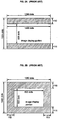
- the number of picture elements of liquid crystal panel 108 is, for example, 1280 dots horizontally and 1024 dots vertically
- an input image signal having picture elements numbering 800 horizontally and 600 vertically is to be displayed on this liquid crystal panel 108 as shown in Fig. 7
- the input image signal is displayed in the center and the periphery is made a frame displayed as, for example, black.
- writing of black-level signals to picture elements corresponding to the frame in the horizontal direction is carried out in the vertical blanking interval rather than in the horizontal blanking interval, and allowing driving of these picture elements in the vertical blanking interval in this way enables normal display of the frame in the horizontal direction even in a case in which the horizontal blanking interval is short and insufficient for driving all of the picture elements in the frame, as in this case, in which the picture elements to be treated as the frame number 480 dots horizontally (1280 dots - 800 dots).
- Source driver 104 is driven at high speed in the vertical blanking interval according to the timing chart shown in Fig. 8. Regarding the horizontal direction at this time, each control for start pulse (DX) 202 and shift clock (CLX) 201 of source driver 104 is executed as shown in Fig. 8 such that source lines 206 turn on only for the portion corresponding to the frame.
- DX start pulse
- CLX shift clock
- start pulse (DX) 202 of source driver 104 is supplied to source driver 104 so as to turn on only the 240 source lines 206 of picture elements in the frame display areas to the left and right in the horizontal direction. Essentially, by conferring this type of start pulse 202, only those picture elements that are intended for execution of frame display can be displayed as frame data, as explained hereinbelow.
- Interval 1 shown in Fig. 8C is the period during which source driver 104 is thus driven so as to turn on source lines 206 only for portions corresponding to the frame in the horizontal direction. Moreover, making enable signal (ENX) 203 of source driver 104 a low-level signal during this interval in which processing of source driver 104 takes place prevents any influence upon image display areas during the processing period of source driver 104.
- ENX enable signal
- shift clock (CLX) 201 of source driver 104 is halted, and during the interval up to completion of writing of frame data in the horizontal direction, the state of source driver 104 is maintained and source lines 206 of areas corresponding to the frame in the horizontal direction remain unchanged in the ON state.
- enable signal (ENX) 203 of source driver 104 is made high level, thereby enabling writing of image signals to picture elements corresponding to the frame in the horizontal direction.
- the supply of image data to picture elements corresponding to the frame in the horizontal direction is enabled by the processing up to this point, and the state of source lines 206 at this time is such that only source lines 206 corresponding to the frame in the horizontal direction to the left and right are maintained in a high-level state.
- writing image signals to picture elements corresponding to the frame in the horizontal direction is executed by initiating drive of gate driver 105 and sequentially turning on gate lines 213 in accordance with start pulse (DY) 209 and shift clock (CLY) 208.
- the drive frequency of gate driver 105 at this time must be a frequency that provides sufficient time to write image signals to the liquid crystal picture elements.
- the image level at this time is made the black level if the frame is to be displayed as black, and, to realize other frame displays (such as a pattern), is made image levels corresponding to such displays.
- interval 2 The interval for writing actual image signals to liquid crystal picture elements is shown as interval 2 in Fig. 8C.
- shift clock (CLX) 201 of source driver 104 is driven and source lines 206 corresponding to the frame in the horizontal direction that were written in interval 2 are reset in interval 3.
- drive is effected such that all source lines 206 become low level by maintaining start pulse (DX) 202 of source driver 104 unchanged at a low level and driving shift clock (CLX) 201 of source driver 104.
- enable signal (ENX) 203 of source driver 104 must be made low level such that no effect appears on the display screen.
- Fig. 8A shows a drive timing chart for the horizontal blanking interval
- Fig. 8B shows a drive timing chart for the vertical blanking interval
- Fig. 9 is a schematic block diagram showing one example of timing control circuit 103 (Fig. 4) that generates each of the timing signals shown in Fig. 8.
- This circuit 103 inputs system clock 109 (phase-locked with vertical and horizontal synchronizing signals 106 and 102 inputted from terminals from PLL circuit 107 in addition to vertical and horizontal synchronizing signals 106 and 102; generates the various timing signals shown in Fig. 8; and consists of clock frequency divider circuit 41, vertical counter 42, decoders 43, 44, 45, 48, 49, and 50, clock switching circuit 46, and horizontal counter 47.
- Clock frequency divider circuit 41 frequency-divides system clocks 109, outputs the four types of clocks CLX1, CLX2, CLY1, and CLY2 shown in Fig. 8, and supplies the clocks to clock switching circuit 46.
- Vertical counter 42 takes vertical synchronizing signal 106 as reset input and counts the frequency divided clocks of clock frequency divider circuit 41.
- Decoders 43, 44, and 45 each detect when the count output of vertical counter 42 reaches a predetermined value and respectively generate start pulse (DY) 209, enable signal (ENY) 210, and clock switching signal (CLY-SEL, CLY-ENABLE) shown in Fig. 8.
- Horizontal counter 47 takes horizontal synchronizing signal 102 as the reset input and counts the frequency divided clocks of clock frequency divider circuit 41. Decoders 48, 49, and 50 each detect when the count output of horizontal counter 47 reaches a predetermined value and respectively output start pulse (DX) 202, enable signal (ENX) 203, and clock switching signal (CLX-SEL, CLX-ENABLE) shown in Fig. 8.
- Clock switching circuit 46 selects and outputs each clock CLY and CLX of Fig. 8 in accordance with each output signal of decoders 45 and 50.
- the details of these components come within the sphere of design items, and further details are therefore not described herein. However, a person knowledgeable in the art would be able to easily design this timing control circuit 103 in accordance with the operation timing chart of Fig. 8.
Landscapes
- Engineering & Computer Science (AREA)
- Physics & Mathematics (AREA)
- Computer Hardware Design (AREA)
- General Physics & Mathematics (AREA)
- Theoretical Computer Science (AREA)
- Chemical & Material Sciences (AREA)
- Crystallography & Structural Chemistry (AREA)
- Liquid Crystal Display Device Control (AREA)
- Control Of Indicators Other Than Cathode Ray Tubes (AREA)
- Transforming Electric Information Into Light Information (AREA)
Applications Claiming Priority (2)
| Application Number | Priority Date | Filing Date | Title |
|---|---|---|---|
| JP8323238A JP2982722B2 (ja) | 1996-12-04 | 1996-12-04 | 映像表示装置 |
| JP323238/96 | 1996-12-04 |
Publications (2)
| Publication Number | Publication Date |
|---|---|
| EP0847194A2 true EP0847194A2 (de) | 1998-06-10 |
| EP0847194A3 EP0847194A3 (de) | 1999-04-21 |
Family
ID=18152554
Family Applications (1)
| Application Number | Title | Priority Date | Filing Date |
|---|---|---|---|
| EP97121206A Withdrawn EP0847194A3 (de) | 1996-12-04 | 1997-12-03 | Steuerung des Anzeigepegels in der Bildbrandbereiche einer Anzeigevorrichtung mit einer Flüssigkristallanzeigetafel |
Country Status (4)
| Country | Link |
|---|---|
| US (1) | US6018331A (de) |
| EP (1) | EP0847194A3 (de) |
| JP (1) | JP2982722B2 (de) |
| CA (1) | CA2223371C (de) |
Cited By (3)
| Publication number | Priority date | Publication date | Assignee | Title |
|---|---|---|---|---|
| EP1111576A2 (de) * | 1999-11-25 | 2001-06-27 | Nec Corporation | Flüssigkristallanzeigevorrichtung und Steuerverfahren dafür |
| WO2003042750A1 (en) * | 2001-11-14 | 2003-05-22 | Polydisplay Asa | Cascading of multi- or bi-stable liquid crystal display elements in large self-organizing scalable low frame rate display boards |
| EP1580726A2 (de) * | 2004-03-24 | 2005-09-28 | Siemens Aktiengesellschaft | Verfahren und Anordnung zur Variation einer Bildwiederholfrequenz |
Families Citing this family (24)
| Publication number | Priority date | Publication date | Assignee | Title |
|---|---|---|---|---|
| JP3129271B2 (ja) * | 1998-01-14 | 2001-01-29 | 日本電気株式会社 | ゲートドライバ回路及びその駆動方法、並びにアクティブマトリクス型液晶表示装置 |
| US6295048B1 (en) * | 1998-09-18 | 2001-09-25 | Compaq Computer Corporation | Low bandwidth display mode centering for flat panel display controller |
| US6879313B1 (en) * | 1999-03-11 | 2005-04-12 | Sharp Kabushiki Kaisha | Shift register circuit, image display apparatus having the circuit, and driving method for LCD devices |
| JP4277148B2 (ja) * | 2000-01-07 | 2009-06-10 | シャープ株式会社 | 液晶表示装置及びその駆動方法 |
| US20010052887A1 (en) * | 2000-04-11 | 2001-12-20 | Yusuke Tsutsui | Method and circuit for driving display device |
| US7034816B2 (en) * | 2000-08-11 | 2006-04-25 | Seiko Epson Corporation | System and method for driving a display device |
| US7425970B1 (en) | 2000-11-08 | 2008-09-16 | Palm, Inc. | Controllable pixel border for a negative mode passive matrix display device |
| US7724270B1 (en) | 2000-11-08 | 2010-05-25 | Palm, Inc. | Apparatus and methods to achieve a variable color pixel border on a negative mode screen with a passive matrix drive |
| US6961029B1 (en) * | 2000-11-08 | 2005-11-01 | Palm, Inc. | Pixel border for improved viewability of a display device |
| US20020067337A1 (en) * | 2000-12-01 | 2002-06-06 | Klink Kristopher Allyn | Liquid crystal display imager and clock reduction method |
| KR100549156B1 (ko) * | 2001-07-23 | 2006-02-06 | 가부시키가이샤 히타치세이사쿠쇼 | 표시 장치 |
| US7164779B2 (en) | 2001-08-06 | 2007-01-16 | Mitsubishi Electric Research Laboratories, Inc. | Privacy-enhanced display device |
| WO2004040544A1 (ja) * | 2002-10-29 | 2004-05-13 | Toshiba Matsushita Display Technology Co., Ltd. | 電圧生成回路 |
| JP3726910B2 (ja) | 2003-07-18 | 2005-12-14 | セイコーエプソン株式会社 | 表示ドライバ及び電気光学装置 |
| JP3722371B2 (ja) * | 2003-07-23 | 2005-11-30 | シャープ株式会社 | シフトレジスタおよび表示装置 |
| US20050195150A1 (en) * | 2004-03-03 | 2005-09-08 | Sharp Kabushiki Kaisha | Display panel and display device |
| KR20060065277A (ko) * | 2004-12-10 | 2006-06-14 | 삼성전자주식회사 | 디스플레이장치 및 그 제어방법 |
| JP2006284708A (ja) * | 2005-03-31 | 2006-10-19 | Sony Corp | 表示パネル、その駆動方法および駆動装置、並びに表示装置 |
| JP2006292925A (ja) * | 2005-04-08 | 2006-10-26 | Matsushita Electric Ind Co Ltd | 液晶表示装置 |
| US20070018999A1 (en) * | 2005-07-25 | 2007-01-25 | Rai Barinder S | Auto-centering of main image |
| CN101297349B (zh) * | 2005-11-04 | 2010-08-18 | 夏普株式会社 | 显示装置及其驱动电路和驱动方法 |
| TWI382388B (zh) * | 2006-05-23 | 2013-01-11 | Au Optronics Corp | 薄膜電晶體液晶顯示器的驅動電路、時序控制器及其驅動方法 |
| US20090278823A1 (en) * | 2008-05-09 | 2009-11-12 | Cheng-Yueh Kuo | Image frame regulation system and image frame regulating method |
| CN103971652B (zh) * | 2013-01-24 | 2016-12-28 | 晨星半导体股份有限公司 | 影像处理方法以及影像处理装置 |
Citations (4)
| Publication number | Priority date | Publication date | Assignee | Title |
|---|---|---|---|---|
| EP0421772A2 (de) * | 1989-10-06 | 1991-04-10 | Canon Kabushiki Kaisha | Anzeigegerät |
| EP0456165A2 (de) * | 1990-05-07 | 1991-11-13 | Kabushiki Kaisha Toshiba | System zur Steuerung einer Flüssigkristallfarbanzeige |
| EP0674207A1 (de) * | 1993-09-09 | 1995-09-27 | Kabushiki Kaisha Toshiba | Anzeigevorrichtung und verfahren zu ihrer steuerung |
| JPH0961788A (ja) * | 1995-08-23 | 1997-03-07 | Nec Corp | 液晶表示装置 |
Family Cites Families (8)
| Publication number | Priority date | Publication date | Assignee | Title |
|---|---|---|---|---|
| JPH0389784A (ja) * | 1989-09-01 | 1991-04-15 | Victor Co Of Japan Ltd | 液晶ライトバルブを用いた画像投影機からの投影画像の画枠形状の補正回路 |
| JP2819695B2 (ja) * | 1989-11-20 | 1998-10-30 | 株式会社富士通ゼネラル | プロジェクタ装置 |
| JPH0455890A (ja) * | 1990-06-25 | 1992-02-24 | Canon Inc | 画像データ制御装置及び表示システム |
| JPH05119734A (ja) * | 1991-10-28 | 1993-05-18 | Canon Inc | 表示制御装置 |
| US5673062A (en) * | 1992-11-06 | 1997-09-30 | Canon Kabushiki Kaisha | Liquid crystal apparatus |
| DE19540146B4 (de) * | 1994-10-27 | 2012-06-21 | Nec Corp. | Flüssigkristallanzeige vom aktiven Matrixtyp mit Treibern für Multimedia-Anwendungen und Ansteuerverfahren dafür |
| JPH08211851A (ja) * | 1995-02-06 | 1996-08-20 | Matsushita Electric Ind Co Ltd | ディスプレイ駆動装置 |
| US5867140A (en) * | 1996-11-27 | 1999-02-02 | Motorola, Inc. | Display system and circuit therefor |
-
1996
- 1996-12-04 JP JP8323238A patent/JP2982722B2/ja not_active Expired - Lifetime
-
1997
- 1997-12-03 CA CA002223371A patent/CA2223371C/en not_active Expired - Fee Related
- 1997-12-03 EP EP97121206A patent/EP0847194A3/de not_active Withdrawn
- 1997-12-04 US US08/985,271 patent/US6018331A/en not_active Expired - Fee Related
Patent Citations (4)
| Publication number | Priority date | Publication date | Assignee | Title |
|---|---|---|---|---|
| EP0421772A2 (de) * | 1989-10-06 | 1991-04-10 | Canon Kabushiki Kaisha | Anzeigegerät |
| EP0456165A2 (de) * | 1990-05-07 | 1991-11-13 | Kabushiki Kaisha Toshiba | System zur Steuerung einer Flüssigkristallfarbanzeige |
| EP0674207A1 (de) * | 1993-09-09 | 1995-09-27 | Kabushiki Kaisha Toshiba | Anzeigevorrichtung und verfahren zu ihrer steuerung |
| JPH0961788A (ja) * | 1995-08-23 | 1997-03-07 | Nec Corp | 液晶表示装置 |
Non-Patent Citations (1)
| Title |
|---|
| PATENT ABSTRACTS OF JAPAN vol. 97, no. 7, 31 July 1997 & JP 09 061788 A (NEC), 7 March 1997 * |
Cited By (5)
| Publication number | Priority date | Publication date | Assignee | Title |
|---|---|---|---|---|
| EP1111576A2 (de) * | 1999-11-25 | 2001-06-27 | Nec Corporation | Flüssigkristallanzeigevorrichtung und Steuerverfahren dafür |
| EP1111576A3 (de) * | 1999-11-25 | 2003-04-09 | Nec Corporation | Flüssigkristallanzeigevorrichtung und Steuerverfahren dafür |
| WO2003042750A1 (en) * | 2001-11-14 | 2003-05-22 | Polydisplay Asa | Cascading of multi- or bi-stable liquid crystal display elements in large self-organizing scalable low frame rate display boards |
| EP1580726A2 (de) * | 2004-03-24 | 2005-09-28 | Siemens Aktiengesellschaft | Verfahren und Anordnung zur Variation einer Bildwiederholfrequenz |
| EP1580726A3 (de) * | 2004-03-24 | 2010-03-17 | Continental Automotive GmbH | Verfahren und Anordnung zur Variation einer Bildwiederholfrequenz |
Also Published As
| Publication number | Publication date |
|---|---|
| CA2223371C (en) | 2000-05-30 |
| US6018331A (en) | 2000-01-25 |
| JP2982722B2 (ja) | 1999-11-29 |
| JPH10161608A (ja) | 1998-06-19 |
| CA2223371A1 (en) | 1998-06-04 |
| EP0847194A3 (de) | 1999-04-21 |
Similar Documents
| Publication | Publication Date | Title |
|---|---|---|
| US6018331A (en) | Frame display control in an image display having a liquid crystal display panel | |
| US6624800B2 (en) | Controller circuit for liquid crystal matrix display devices | |
| US20120092392A1 (en) | Liquid Crystal Display Apparatus | |
| US7012598B2 (en) | Liquid crystal display device and method for operating the same | |
| US6128045A (en) | Flat-panel display device and display method | |
| US7663591B2 (en) | Display device and method of driving same | |
| US6362804B1 (en) | Liquid crystal display with picture displaying function for displaying a picture in an aspect ratio different from the normal aspect ratio | |
| CA2164803C (en) | Method and circuit for driving picture display devices | |
| JP2005049775A (ja) | 電気光学装置、駆動回路及び方法、画像信号生成装置、並びに電子機器 | |
| US6597336B1 (en) | Display apparatus and method | |
| WO2006134853A1 (ja) | 表示装置及びその駆動制御装置、並びに走査信号線駆動方法及び駆動回路 | |
| JP3016369B2 (ja) | 映像表示装置 | |
| JP3623304B2 (ja) | 液晶表示装置 | |
| JP2004233808A (ja) | 液晶装置及びその駆動方法並びに電子機器 | |
| JP4507630B2 (ja) | 光学機能装置及び光学表示方法 | |
| JPH03285479A (ja) | ドットマトリクス表示素子を用いた画像表示装置 | |
| JP3242297B2 (ja) | 画像表示装置 | |
| JP2004233807A (ja) | 液晶装置及びその駆動方法並びに電子機器 | |
| JPH1114967A (ja) | 表示制御方法および液晶表示装置、投写型表示装置並びに電子機器 | |
| JP3945733B2 (ja) | 画像表示装置 | |
| KR101016736B1 (ko) | 액정표시장치와 그의 구동방법 | |
| KR0173715B1 (ko) | 투사형 화상표시장치의 화소구동회로 | |
| JPH09270976A (ja) | 液晶表示装置 | |
| JP4479154B2 (ja) | 電気光学装置及びその駆動方法並びに電子機器 | |
| JP3602395B2 (ja) | 投射型の表示装置 |
Legal Events
| Date | Code | Title | Description |
|---|---|---|---|
| PUAI | Public reference made under article 153(3) epc to a published international application that has entered the european phase |
Free format text: ORIGINAL CODE: 0009012 |
|
| AK | Designated contracting states |
Kind code of ref document: A2 Designated state(s): DE FR GB |
|
| AX | Request for extension of the european patent |
Free format text: AL;LT;LV;MK;RO;SI |
|
| PUAL | Search report despatched |
Free format text: ORIGINAL CODE: 0009013 |
|
| AK | Designated contracting states |
Kind code of ref document: A3 Designated state(s): AT BE CH DE DK ES FI FR GB GR IE IT LI LU MC NL PT SE |
|
| AX | Request for extension of the european patent |
Free format text: AL;LT;LV;MK;RO;SI |
|
| 17P | Request for examination filed |
Effective date: 19990309 |
|
| AKX | Designation fees paid |
Free format text: DE FR GB |
|
| STAA | Information on the status of an ep patent application or granted ep patent |
Free format text: STATUS: THE APPLICATION HAS BEEN WITHDRAWN |
|
| 18W | Application withdrawn |
Withdrawal date: 20000808 |