EP0840237A1 - Datenprozessorsynchronisation mit externem Bus - Google Patents
Datenprozessorsynchronisation mit externem Bus Download PDFInfo
- Publication number
- EP0840237A1 EP0840237A1 EP97118442A EP97118442A EP0840237A1 EP 0840237 A1 EP0840237 A1 EP 0840237A1 EP 97118442 A EP97118442 A EP 97118442A EP 97118442 A EP97118442 A EP 97118442A EP 0840237 A1 EP0840237 A1 EP 0840237A1
- Authority
- EP
- European Patent Office
- Prior art keywords
- signal
- data processor
- state
- data
- clock signal
- Prior art date
- Legal status (The legal status is an assumption and is not a legal conclusion. Google has not performed a legal analysis and makes no representation as to the accuracy of the status listed.)
- Granted
Links
Images







Classifications
-
- G—PHYSICS
- G06—COMPUTING OR CALCULATING; COUNTING
- G06F—ELECTRIC DIGITAL DATA PROCESSING
- G06F13/00—Interconnection of, or transfer of information or other signals between, memories, input/output devices or central processing units
- G06F13/38—Information transfer, e.g. on bus
- G06F13/42—Bus transfer protocol, e.g. handshake; Synchronisation
- G06F13/4204—Bus transfer protocol, e.g. handshake; Synchronisation on a parallel bus
- G06F13/4208—Bus transfer protocol, e.g. handshake; Synchronisation on a parallel bus being a system bus, e.g. VME bus, Futurebus, Multibus
- G06F13/4217—Bus transfer protocol, e.g. handshake; Synchronisation on a parallel bus being a system bus, e.g. VME bus, Futurebus, Multibus with synchronous protocol
Definitions
- the present invention is embodied in a data processor which employs the following organization.
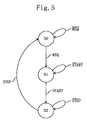
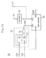
- the data processor comprises (a) a clock generation circuit for generating from an external clock signal an internal clock signal having a frequency which is an integral multiple of that of the external clock signal, (b) a processing means for processing data in synchronization with the internal clock signal, (c) a bus interface for controlling data transmission between the processing means and the external device, (d) a start signal generation circuit for generating a start signal which selects, from among a plurality of sub-periods resulting from division of one cycle period of the external clock signal and each having a length equivalent to one cycle period of the internal clock signal, a sub-period at a corresponding position to the setup time of the external device, and (e) a state control circuit for controlling an internal state of the data processor in order that the data processor may make a transition to a state of transmission when the state control circuit receives the start signal after having received a transmission request signal issued from the processing means in synchronization with the internal clock signal
- the bus interface 20 controls the transmission of data between the CPU 12 and the external device 2, in other word such data transmission is controlled by the bus interface 20 to start in synchronization with the rising edge of SIGNAL ECLK.
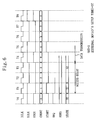
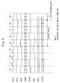
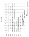
- the start signal generation circuit 30 is a circuit for generating a start signal START which selects, from among four sub-periods as a result of equal-division of one cycle period of SIGNAL ECLK, a sub-period at a corresponding position to the setup time of the external device 2. The selecting of a sub-period is carried out based on a set value signal SET supplied from the CPU 12 to the start signal generation circuit 30.
Landscapes
- Engineering & Computer Science (AREA)
- Theoretical Computer Science (AREA)
- Physics & Mathematics (AREA)
- General Engineering & Computer Science (AREA)
- General Physics & Mathematics (AREA)
- Information Transfer Systems (AREA)
Applications Claiming Priority (2)
| Application Number | Priority Date | Filing Date | Title |
|---|---|---|---|
| JP28635696 | 1996-10-29 | ||
| JP286356/96 | 1996-10-29 |
Publications (2)
| Publication Number | Publication Date |
|---|---|
| EP0840237A1 true EP0840237A1 (de) | 1998-05-06 |
| EP0840237B1 EP0840237B1 (de) | 2007-01-03 |
Family
ID=17703326
Family Applications (1)
| Application Number | Title | Priority Date | Filing Date |
|---|---|---|---|
| EP97118442A Expired - Lifetime EP0840237B1 (de) | 1996-10-29 | 1997-10-23 | Datenprozessorsynchronisation mit externem Bus |
Country Status (3)
| Country | Link |
|---|---|
| US (1) | US5940599A (de) |
| EP (1) | EP0840237B1 (de) |
| DE (1) | DE69737179T2 (de) |
Cited By (1)
| Publication number | Priority date | Publication date | Assignee | Title |
|---|---|---|---|---|
| FR2870368A1 (fr) * | 2004-01-27 | 2005-11-18 | Atmel Corp | Procede et dispositif pour piloter de multiples peripheriques avec des frequences d'horloge differentes dans un circuit integre |
Families Citing this family (5)
| Publication number | Priority date | Publication date | Assignee | Title |
|---|---|---|---|---|
| US6052754A (en) * | 1998-05-14 | 2000-04-18 | Vlsi Technology, Inc. | Centrally controlled interface scheme for promoting design reusable circuit blocks |
| US6651199B1 (en) * | 2000-06-22 | 2003-11-18 | Xilinx, Inc. | In-system programmable flash memory device with trigger circuit for generating limited duration program instruction |
| FR2839827B1 (fr) * | 2002-05-14 | 2005-07-15 | St Microelectronics Sa | Circuit de detection de depart, circuit de detection d'arret, et circuit de detection de donnees transmises selon le protocole iic |
| WO2006121437A1 (en) * | 2005-05-10 | 2006-11-16 | Telairity Semiconductor, Inc. | Method and apparatus for clock synchronization between a processor and external devices |
| US20060259807A1 (en) * | 2005-05-10 | 2006-11-16 | Telairity Semiconductor, Inc. | Method and apparatus for clock synchronization between a processor and external devices |
Citations (3)
| Publication number | Priority date | Publication date | Assignee | Title |
|---|---|---|---|---|
| EP0497441A2 (de) * | 1991-01-28 | 1992-08-05 | Advanced Micro Devices, Inc. | Verbessertes synchronisches Taktsystem für Mikroprozessor |
| EP0645717A1 (de) * | 1993-09-07 | 1995-03-29 | Motorola, Inc. | System und Verfahren für Datensynchronisierung |
| US5485602A (en) * | 1993-12-27 | 1996-01-16 | Motorola, Inc. | Integrated circuit having a control signal for identifying coinciding active edges of two clock signals |
Family Cites Families (4)
| Publication number | Priority date | Publication date | Assignee | Title |
|---|---|---|---|---|
| JPH0285951A (ja) * | 1988-06-08 | 1990-03-27 | Nec Corp | 入出力バス・サイクル制御方式 |
| US5272729A (en) * | 1991-09-20 | 1993-12-21 | International Business Machines Corporation | Clock signal latency elimination network |
| JP2770656B2 (ja) * | 1992-05-11 | 1998-07-02 | ヤマハ株式会社 | 集積回路装置 |
| US5811998A (en) * | 1993-01-28 | 1998-09-22 | Digital Equipment Corporation | State machine phase lock loop |
-
1997
- 1997-10-23 EP EP97118442A patent/EP0840237B1/de not_active Expired - Lifetime
- 1997-10-23 DE DE69737179T patent/DE69737179T2/de not_active Expired - Lifetime
- 1997-10-24 US US08/957,160 patent/US5940599A/en not_active Expired - Lifetime
Patent Citations (3)
| Publication number | Priority date | Publication date | Assignee | Title |
|---|---|---|---|---|
| EP0497441A2 (de) * | 1991-01-28 | 1992-08-05 | Advanced Micro Devices, Inc. | Verbessertes synchronisches Taktsystem für Mikroprozessor |
| EP0645717A1 (de) * | 1993-09-07 | 1995-03-29 | Motorola, Inc. | System und Verfahren für Datensynchronisierung |
| US5485602A (en) * | 1993-12-27 | 1996-01-16 | Motorola, Inc. | Integrated circuit having a control signal for identifying coinciding active edges of two clock signals |
Cited By (2)
| Publication number | Priority date | Publication date | Assignee | Title |
|---|---|---|---|---|
| FR2870368A1 (fr) * | 2004-01-27 | 2005-11-18 | Atmel Corp | Procede et dispositif pour piloter de multiples peripheriques avec des frequences d'horloge differentes dans un circuit integre |
| US7162003B2 (en) | 2004-01-27 | 2007-01-09 | Atmel Corporation | Method and apparatus for driving multiple peripherals with different clock frequencies in an integrated circuit |
Also Published As
| Publication number | Publication date |
|---|---|
| DE69737179D1 (de) | 2007-02-15 |
| EP0840237B1 (de) | 2007-01-03 |
| DE69737179T2 (de) | 2007-04-19 |
| US5940599A (en) | 1999-08-17 |
Similar Documents
| Publication | Publication Date | Title |
|---|---|---|
| US4523274A (en) | Data processing system with processors having different processing speeds sharing a common bus | |
| US4591979A (en) | Data-flow-type digital processing apparatus | |
| JPS625406A (ja) | 状態装置 | |
| EP0242879B1 (de) | Datenprozessor mit Wartesteuerung, die Hochgeschwindigkeitszugriff gestattet | |
| WO2001035234A9 (en) | Generic serial port architecture and system | |
| EP0273642B1 (de) | Einrichtung zum Lesen von Daten aus einem Speicher | |
| US5940599A (en) | Data processor | |
| JPH09106682A (ja) | 同期式メモリのデータ出力バッファ制御方法 | |
| US4380736A (en) | Peripheral interface adapter circuit for counter synchronization | |
| KR100313945B1 (ko) | 다단 인터럽트 제어 장치 | |
| JP3450667B2 (ja) | データプロセッサ | |
| US4459688A (en) | Access request selecting circuit | |
| JPH03144990A (ja) | メモリ装置 | |
| JP2000099188A (ja) | クロック切替回路 | |
| US6794891B2 (en) | Semiconductor integrated circuit | |
| JPH05100844A (ja) | マイクロ・プロセツサのプログラムウエイト制御回路 | |
| US6928025B1 (en) | Synchronous integrated memory | |
| JPH1115783A (ja) | 同期回路 | |
| JP2001035148A (ja) | データ処理装置 | |
| JP2655509B2 (ja) | シリアル/パラレル変換回路 | |
| JP2000163155A (ja) | データ処理回路 | |
| JP2870812B2 (ja) | 並列処理プロセッサ | |
| JP2517943B2 (ja) | タイマ装置 | |
| JP2668215B2 (ja) | マイクロコンピユータ | |
| JPH10124455A (ja) | シリアル通信回路 |
Legal Events
| Date | Code | Title | Description |
|---|---|---|---|
| PUAI | Public reference made under article 153(3) epc to a published international application that has entered the european phase |
Free format text: ORIGINAL CODE: 0009012 |
|
| AK | Designated contracting states |
Kind code of ref document: A1 Designated state(s): DE FR |
|
| AX | Request for extension of the european patent |
Free format text: AL;LT;LV;RO;SI |
|
| 17P | Request for examination filed |
Effective date: 19980612 |
|
| AKX | Designation fees paid |
Free format text: DE FR |
|
| RBV | Designated contracting states (corrected) |
Designated state(s): DE FR |
|
| GRAP | Despatch of communication of intention to grant a patent |
Free format text: ORIGINAL CODE: EPIDOSNIGR1 |
|
| GRAS | Grant fee paid |
Free format text: ORIGINAL CODE: EPIDOSNIGR3 |
|
| GRAA | (expected) grant |
Free format text: ORIGINAL CODE: 0009210 |
|
| AK | Designated contracting states |
Kind code of ref document: B1 Designated state(s): DE FR |
|
| REF | Corresponds to: |
Ref document number: 69737179 Country of ref document: DE Date of ref document: 20070215 Kind code of ref document: P |
|
| ET | Fr: translation filed | ||
| PLBE | No opposition filed within time limit |
Free format text: ORIGINAL CODE: 0009261 |
|
| STAA | Information on the status of an ep patent application or granted ep patent |
Free format text: STATUS: NO OPPOSITION FILED WITHIN TIME LIMIT |
|
| 26N | No opposition filed |
Effective date: 20071005 |
|
| PGFP | Annual fee paid to national office [announced via postgrant information from national office to epo] |
Ref country code: DE Payment date: 20091015 Year of fee payment: 13 |
|
| PGFP | Annual fee paid to national office [announced via postgrant information from national office to epo] |
Ref country code: FR Payment date: 20091029 Year of fee payment: 13 |
|
| PG25 | Lapsed in a contracting state [announced via postgrant information from national office to epo] |
Ref country code: FR Free format text: LAPSE BECAUSE OF NON-PAYMENT OF DUE FEES Effective date: 20101102 |
|
| REG | Reference to a national code |
Ref country code: FR Ref legal event code: ST Effective date: 20110630 |
|
| REG | Reference to a national code |
Ref country code: DE Ref legal event code: R119 Ref document number: 69737179 Country of ref document: DE Effective date: 20110502 |
|
| PG25 | Lapsed in a contracting state [announced via postgrant information from national office to epo] |
Ref country code: DE Free format text: LAPSE BECAUSE OF NON-PAYMENT OF DUE FEES Effective date: 20110502 |