EP0829881B1 - Wordline drive circuit for flash EEPROM memory - Google Patents
Wordline drive circuit for flash EEPROM memory Download PDFInfo
- Publication number
- EP0829881B1 EP0829881B1 EP97830445A EP97830445A EP0829881B1 EP 0829881 B1 EP0829881 B1 EP 0829881B1 EP 97830445 A EP97830445 A EP 97830445A EP 97830445 A EP97830445 A EP 97830445A EP 0829881 B1 EP0829881 B1 EP 0829881B1
- Authority
- EP
- European Patent Office
- Prior art keywords
- node
- transistor
- voltage
- pull
- gate
- Prior art date
- Legal status (The legal status is an assumption and is not a legal conclusion. Google has not performed a legal analysis and makes no representation as to the accuracy of the status listed.)
- Expired - Lifetime
Links
- 230000015654 memory Effects 0.000 title claims description 19
- 230000000694 effects Effects 0.000 description 9
- XUIMIQQOPSSXEZ-UHFFFAOYSA-N Silicon Chemical compound [Si] XUIMIQQOPSSXEZ-UHFFFAOYSA-N 0.000 description 5
- 229910052710 silicon Inorganic materials 0.000 description 5
- 239000010703 silicon Substances 0.000 description 5
- 238000010586 diagram Methods 0.000 description 4
- 230000009471 action Effects 0.000 description 3
- 230000008901 benefit Effects 0.000 description 3
- 230000009467 reduction Effects 0.000 description 3
- 230000000630 rising effect Effects 0.000 description 3
- 238000005516 engineering process Methods 0.000 description 2
- 230000007704 transition Effects 0.000 description 2
- 230000002411 adverse Effects 0.000 description 1
- 230000006399 behavior Effects 0.000 description 1
- 230000008878 coupling Effects 0.000 description 1
- 238000010168 coupling process Methods 0.000 description 1
- 238000005859 coupling reaction Methods 0.000 description 1
- 230000001186 cumulative effect Effects 0.000 description 1
- 230000001934 delay Effects 0.000 description 1
- 230000006870 function Effects 0.000 description 1
- 238000009413 insulation Methods 0.000 description 1
- 238000000034 method Methods 0.000 description 1
- 230000008569 process Effects 0.000 description 1
- 230000001737 promoting effect Effects 0.000 description 1
- 239000004065 semiconductor Substances 0.000 description 1
- 238000006467 substitution reaction Methods 0.000 description 1
Images


Classifications
-
- G—PHYSICS
- G11—INFORMATION STORAGE
- G11C—STATIC STORES
- G11C16/00—Erasable programmable read-only memories
- G11C16/02—Erasable programmable read-only memories electrically programmable
- G11C16/06—Auxiliary circuits, e.g. for writing into memory
-
- G—PHYSICS
- G11—INFORMATION STORAGE
- G11C—STATIC STORES
- G11C16/00—Erasable programmable read-only memories
- G11C16/02—Erasable programmable read-only memories electrically programmable
- G11C16/06—Auxiliary circuits, e.g. for writing into memory
- G11C16/10—Programming or data input circuits
- G11C16/12—Programming voltage switching circuits
-
- G—PHYSICS
- G11—INFORMATION STORAGE
- G11C—STATIC STORES
- G11C8/00—Arrangements for selecting an address in a digital store
- G11C8/08—Word line control circuits, e.g. drivers, boosters, pull-up circuits, pull-down circuits, precharging circuits, for word lines
Definitions
- This invention broadly relates to drive circuits for semiconductor memories and more particularly concerns a row drive circuit for low voltage Flash EEPROM memories.
- variable signals within an extended voltage range are intended to be used in the various operation modes of the memory, such as the read or programming or erasure operations.
- the logic signals are control signals and are variable between ground voltage, as indicated by GND, and the supply voltage, as indicated by VDD.
- the normal supply voltage in these circuits which are also designated as low voltage or low power circuits, is presently of about 3.3 volts, while the voltage used for performing operations such as internal programming or erasure operations can also reach 12 volts (for instance, 5 volts for read operations).
- this entails the need to implement various circuits on the chip to generate such higher voltages starting from the low supply voltage of 3.3 volts, and, on the other side, this entails the need to implement suitable circuits within the memory itself adapted to handle or manage these voltages higher than the supply voltage, without introducing time delays incompatible with proper operation of the memory and consequently without affecting its access times.
- the essential requirement of these circuits therefore, is related to their operation speed: these circuits are defined as voltage translators.
- This invention is not aimed at generating such operation voltages higher than the supply voltage, but it is an object thereof to handle these voltages in very fast manner, while also a space saving is achieved on the silicon area.
- the main but, of course, not exclusive application of this invention is to be identified in a row drive circuit for Flash EEPROM memories, by operating as a voltage translator circuit designed to couple such above mentioned read voltages to selected rows or wordlines of the memory.
- the read operation are carried out by driving the selected wordline to 5 volts and all non-selected wordlines to ground GND.
- the concerned wordlines should be driven to other voltages, typically in the range -9 volts to 12 volts.
- High voltage transistors should be used, therefore, in said row drive circuits, in order to accommodate these voltages noticeably higher than the supply voltage.
- said high voltage transistors offer rather poor performances with respect to low voltage transistors, as it is well known to those skilled in the art, due to the noticeable thickness of the required gate oxide.
- the row drive circuit should drive the selected wordlines in a very fast manner, even if high voltage transistor are employed, due to the fact that any delay in coupling the wordline driving voltages directly and adversely affects the memory access time.
- EP-A-0 356 650 discloses a circuit for applying reading, programming and erasing voltages to a worldline in a floating-gate type EEPROM cell array comprising a positive voltage switching circuit, at least one first isolating transistor and a second isolating transistor.
- the positive voltage switching circuit may include an inverter with a feedback transistor and a third isolating transistor.
- the wordline is connected through node 1 to voltage VX and to ground VXGND, respectively, by means of a P-channel transistor pull-up 3 and a N-channel transistor pull-down 2, effectively operating as switches.
- the gate region of transistor pull-down 2 is connected to input node 16, while the gate region of transistor pull-up 3 is connected to node 6.
- a feedback P-channel transistor TP4 is inserted between the operation voltage VX and the gate region of transistor pull-up 3, on node 6. The gate region of feedback transistor TP4 is directly driven by the wordline.
- transistor TP4 Since transistor TP4 is inserted between voltage VX and the gate region of transistor pull-up 3 through node 6, transistor TP4 upon turning on will raise the voltage on node 6 to VX, with the resulting consequence that transistor pull-up 3 will be completely turned off. In this manner, the wordline is perfectly connected to VXGND through transistor pull-down 2 which is on and it is perfectly insulated from voltage VX by means of transistor pull-up 3 which is off.
- a decoupling transistor TN1 is inserted between node 6 and node 16.
- a logic state 1 When the selection signal toggles to logic state 0, a logic state 1 will be established at the output of the inverter circuit BUFF and again a logic state 0 will be established at the output of the NAND gate circuit, on node 16.
- a 0 logic voltage on node 16 when applied to the gate region of transistor pull-down 2, will force the latter to turn off with consequent insulation or decoupling of the wordline from ground VXGND.
- this logic voltage 0 is applied though transistor TN1 and node 6 to the gate region of transistor pull-up 3 and will force it to turn on, thereby raising the wordline voltage up to VX.
- the concerned wordline is connected to the gate region of the feedback transistor TP4, as the wordline voltage is raised, the conduction capability of transistor TP4 is lowered down to the point that said transistor is turned off, which occurs when the wordline is raised just to voltage VX.
- transistor pull-up 3 is on and the concerned wordline is directly connected to voltage VX and completely insulated by means of said transistor pull-up 3 in off condition.
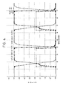
- this invention suggests to adopt the circuit approach shown in Figure 3.
- the concerned wordline is again connected to operation voltage VX by means of a P-channel transistor pull-up 3 and to ground VXGND by means of a N-channel transistor pull-down 2.
- a feedback transistor TP4 is provided, the gate region of which is directly driven by the wordline, inserted between voltage VX and the gate region of transistor pull-up 3, through node 6.
- This circuit is substantially distinguished with respect to the known circuit by means of a further N-channel feedback transistor TN5, the gate of which is again directly driven by the wordline, inserted between node 6, more precisely the gate region of transistor pull-up 3, and the gate region of transistor pull-down 2.
- a N-channel transistor TN1 is inserted between node 6 and ground, said transistor TN1 having its gate region driven by said node 6 and consequently by the same selection signal upon a single inversion.
- transistor TN5 When transistor TN5 is considered, it can be observed that a voltage of 0 volt is established on node 0 and again a voltage of 0 volt is established on node 6, as above already seen, due to the on condition of transistor TN1.
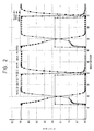
- transistor pull-up 3 Since node 6 is at 0 level and transistor pull-down 2 is in off condition, transistor pull-up 3 will be turned on and it will cause the wordline to begin to rise to voltage VX. By rising to voltage VX, the wordline will cause the feedback transistor TP4 to be turned off through node 18. On the other hand, a higher voltage on node 18 will entail a higher voltage on the gate region of N-channel transistor TN5, but, since a 0 logic level exists both on node 6 and on node 0, namely at the ends of this transistor, the on condition of transistor TN5 will have no effect. As a final result, the concerned wordline will be raised to voltage VX and will be completely decoupled from voltage VXGND.
- node 5 When a switch over operation in the opposite direction is to be carried out, when the selection signal is turned from a 0 logic level to a 1 logic level, node 5 will take up the inverted level 0 and, as a result, transistor TN1 will be turned off and will clear node 6, that is to say it will decouple it from ground voltage GND. Following a further inversion of the signal effected by inverter circuit BUFF, node 0 will turn to level 1 and it will drive the gate region of transistor pull-down 2 so as to turn it on, while the voltage on node 0 will be completely translated to node 6 through the second feed-back transistor TN5. In fact, since voltage VX resulting from the previous switch over operation is still applied to the gate region of transistor TN5 from node 18 and from the concerned wordline, transistor TN5 is still on.
- the wordline is still at voltage VX and transistor TN5 is on.
- the signal of 0 logic level that is prevailing on node 0 not only turns transistor pull-down 2 on - and this is its main object - but it also transfers a charge of a certain amount to node 6 and in this manner it succeeds in slightly raising the voltage of node 6.
- node 6 rises to a level slightly higher than the lever it would reach in absence of transistor TN5.
- a double effect is obtained, namely to aid and to accelerate turning P-channel transistor pull-up 3 off, since it is connected to its gate region.
- the following operation pattern is established: the voltage on node 6 is rising, transistor pull-down 2 is turned on thereby aiming at lowering the wordline voltage.
- the voltage is near to 0, it begins turning transistor TN5 off, but it should be observed that an initial trigger action occurs that enables the turning action on transistor pull-up 3 to be started and consequently to be advanced by a small amount, thereby reducing the transition time.
- transistor pull-up 3 is turning off, and, therefore, the voltage of the wordline is being lowered to 0: as it gets nearer and nearer to 0, it turns the second N-channel feedback transistor TN5 off, but it also turns the first feedback transistor TN4 on, which, in turn, completes turning transistor pull-up 3 off.
- transistor pull-up 3 is turned off and transistor pull-down 2 is turned on, the wordline is decoupled from voltage VX and is coupled to voltage VXGND.
- this circuit just consists in exploiting the above described second feedback effect between node 0 and node 6: this feedback effect is assured by transistor TN5 that, in transition from 0 to 1, utilises its pre-existing conductive condition connected with the pre-existing condition of the wordline.
- Transistor PN5 does not receive its control signal from the output end; but it receives such signal from the input end of the circuit, with an advance time, thereby promoting the above defined starting effect.
- a further advantage of the approach according to this invention connected with the substitution of a NOR gate circuit for the NAND gate circuit, is gained in reducing the silicon area needed for its implementation.
- the row drive circuits in the memory topology should have the same Y dimension as the memory array. This entails that any reduction achieved in the X dimension of the circuit will result into a more relevant reduction in its comprehensive area, since such a reduction will be extended over the whole Y dimension of the circuit. Then, when it is desired to save silicon area, it is substantially important to design the concerned drive circuits with their width dimensions as much compact as possible.
- the difference between the conventional approach and the approach according to this invention has been investigated by adding all W values together and it has been found that the approach according to this invention entails a cumulative W dimension smaller than the one of a conventional approach: this means a two-fold advantage in terms of better performances with a smaller silicon area.
Landscapes
- Engineering & Computer Science (AREA)
- Microelectronics & Electronic Packaging (AREA)
- Read Only Memory (AREA)
- Logic Circuits (AREA)
- Control Of Indicators Other Than Cathode Ray Tubes (AREA)
Applications Claiming Priority (2)
| Application Number | Priority Date | Filing Date | Title |
|---|---|---|---|
| ITRM960626 | 1996-09-13 | ||
| IT96RM000626A IT1285894B1 (it) | 1996-09-13 | 1996-09-13 | Circuito di pilotaggio di riga per memorie flash eeprom a bassa tensione. |
Publications (3)
| Publication Number | Publication Date |
|---|---|
| EP0829881A2 EP0829881A2 (en) | 1998-03-18 |
| EP0829881A3 EP0829881A3 (en) | 1999-07-07 |
| EP0829881B1 true EP0829881B1 (en) | 2003-03-26 |
Family
ID=11404419
Family Applications (1)
| Application Number | Title | Priority Date | Filing Date |
|---|---|---|---|
| EP97830445A Expired - Lifetime EP0829881B1 (en) | 1996-09-13 | 1997-09-10 | Wordline drive circuit for flash EEPROM memory |
Country Status (6)
| Country | Link |
|---|---|
| EP (1) | EP0829881B1 (cg-RX-API-DMAC7.html) |
| JP (1) | JP4519953B2 (cg-RX-API-DMAC7.html) |
| KR (1) | KR100497688B1 (cg-RX-API-DMAC7.html) |
| DE (1) | DE69720126T2 (cg-RX-API-DMAC7.html) |
| IT (1) | IT1285894B1 (cg-RX-API-DMAC7.html) |
| SG (1) | SG67418A1 (cg-RX-API-DMAC7.html) |
Families Citing this family (6)
| Publication number | Priority date | Publication date | Assignee | Title |
|---|---|---|---|---|
| JP3466593B2 (ja) * | 2001-09-20 | 2003-11-10 | 沖電気工業株式会社 | 電圧トランスレータ回路 |
| JP3410084B2 (ja) | 2001-09-20 | 2003-05-26 | 沖電気工業株式会社 | 電圧トランスレータ |
| JP3532181B2 (ja) | 2001-11-21 | 2004-05-31 | 沖電気工業株式会社 | 電圧トランスレータ |
| WO2010076833A1 (en) * | 2008-12-31 | 2010-07-08 | Fabio Pellizzer | Word-line driver including pull-up resistor and pull-down transistor |
| GB2471572B (en) * | 2009-07-02 | 2015-04-22 | Advanced Risc Mach Ltd | Voltage level shifter |
| US8908439B2 (en) * | 2012-09-07 | 2014-12-09 | Taiwan Semiconductor Manufacturing Co., Ltd. | Adaptive word-line boost driver |
Family Cites Families (5)
| Publication number | Priority date | Publication date | Assignee | Title |
|---|---|---|---|---|
| US4823318A (en) * | 1988-09-02 | 1989-04-18 | Texas Instruments Incorporated | Driving circuitry for EEPROM memory cell |
| DE69126234T2 (de) * | 1990-04-23 | 1997-11-06 | Texas Instruments Inc | Wortleitungstreiberschaltung für nichtflüchtiges Speicherzellenarray |
| JPH06338193A (ja) * | 1993-05-28 | 1994-12-06 | Hitachi Ltd | 不揮発性半導体記憶装置 |
| JPH07235190A (ja) * | 1994-02-24 | 1995-09-05 | Sony Corp | 半導体不揮発性記憶装置 |
| KR0170293B1 (ko) * | 1995-12-29 | 1999-03-30 | 김광호 | 이.이.피.롬 장치 |
-
1996
- 1996-09-13 IT IT96RM000626A patent/IT1285894B1/it active IP Right Grant
-
1997
- 1997-09-10 EP EP97830445A patent/EP0829881B1/en not_active Expired - Lifetime
- 1997-09-10 DE DE69720126T patent/DE69720126T2/de not_active Expired - Lifetime
- 1997-09-11 SG SG1997003355A patent/SG67418A1/en unknown
- 1997-09-12 KR KR1019970047089A patent/KR100497688B1/ko not_active Expired - Lifetime
- 1997-09-16 JP JP25109697A patent/JP4519953B2/ja not_active Expired - Lifetime
Also Published As
| Publication number | Publication date |
|---|---|
| DE69720126D1 (de) | 2003-04-30 |
| IT1285894B1 (it) | 1998-06-24 |
| EP0829881A2 (en) | 1998-03-18 |
| JPH10149693A (ja) | 1998-06-02 |
| EP0829881A3 (en) | 1999-07-07 |
| ITRM960626A1 (it) | 1998-03-13 |
| KR100497688B1 (ko) | 2005-09-08 |
| JP4519953B2 (ja) | 2010-08-04 |
| KR19980024604A (ko) | 1998-07-06 |
| DE69720126T2 (de) | 2003-12-04 |
| SG67418A1 (en) | 1999-09-21 |
Similar Documents
| Publication | Publication Date | Title |
|---|---|---|
| US5825205A (en) | Level-shift circuit for driving word lines of negative gate erasable type flash memory | |
| KR910005602B1 (ko) | 어드레스 변환 검출에 따른 출력버퍼의 프리챠아지 제어방법 | |
| US5594687A (en) | Completely complementary MOS memory cell with tunneling through the NMOS and PMOS transistors during program and erase | |
| US6717858B2 (en) | Non-volatile semiconductor memory device in which one page is set for a plurality of memory cell arrays | |
| US6774704B2 (en) | Control circuit for selecting the greater of two voltage signals | |
| US5512845A (en) | Bootstrap circuit | |
| KR102114574B1 (ko) | 레벨 시프터 및 반도체 장치 | |
| US4720816A (en) | Programming of an EPROM | |
| US6259631B1 (en) | Row drive circuit equipped with feedback transistors for low voltage flash EEPROM memories | |
| US6064623A (en) | Row decoder having global and local decoders in flash memory devices | |
| US5708604A (en) | Dynamic selection control in a memory | |
| EP0829881B1 (en) | Wordline drive circuit for flash EEPROM memory | |
| KR100758885B1 (ko) | 플래시 메모리용 고속 디코더 | |
| JPH06208794A (ja) | 立上げ時に定状態であるメモリセル | |
| US6111792A (en) | Non-volatile semiconductor memory device for selective cell flash erasing/programming | |
| KR940005694B1 (ko) | 전기적으로 소거 및 프로그램이 가능한 반도체 메모리장치의 프로그램 최적화회로 및 방법 | |
| KR100390944B1 (ko) | 플래쉬 메모리 장치 | |
| US6343031B1 (en) | Semiconductor memory device | |
| US5917354A (en) | Circuit for resetting output of positive/negative high voltage generating circuit to VCC/VSS | |
| KR100255519B1 (ko) | 안정한 데이터 래치 동작을 위한 에스램 및 그 구동방법 | |
| US7710806B2 (en) | Memory device and method for improving speed at which data is read from non-volatile memory | |
| US5515322A (en) | Semiconductor memory device equipped with sense amplifiers selectively activated with column address decoded signals | |
| KR100335780B1 (ko) | 네가티브 부스팅 회로 | |
| KR100335772B1 (ko) | 플래시 메모리의 로우디코더 회로 | |
| KR100247648B1 (ko) | 로오 디코더 회로 |
Legal Events
| Date | Code | Title | Description |
|---|---|---|---|
| PUAI | Public reference made under article 153(3) epc to a published international application that has entered the european phase |
Free format text: ORIGINAL CODE: 0009012 |
|
| AK | Designated contracting states |
Kind code of ref document: A2 Designated state(s): DE FR GB IT NL |
|
| PUAL | Search report despatched |
Free format text: ORIGINAL CODE: 0009013 |
|
| AK | Designated contracting states |
Kind code of ref document: A3 Designated state(s): AT BE CH DE DK ES FI FR GB GR IE IT LI LU MC NL PT SE |
|
| 17P | Request for examination filed |
Effective date: 19991112 |
|
| AKX | Designation fees paid |
Free format text: DE FR GB IT NL |
|
| RAP1 | Party data changed (applicant data changed or rights of an application transferred) |
Owner name: TEXAS INSTRUMENTS ITALIA S.P.A. Owner name: TEXAS INSTRUMENTS INCORPORATED |
|
| 17Q | First examination report despatched |
Effective date: 20011018 |
|
| GRAH | Despatch of communication of intention to grant a patent |
Free format text: ORIGINAL CODE: EPIDOS IGRA |
|
| GRAH | Despatch of communication of intention to grant a patent |
Free format text: ORIGINAL CODE: EPIDOS IGRA |
|
| GRAA | (expected) grant |
Free format text: ORIGINAL CODE: 0009210 |
|
| AK | Designated contracting states |
Designated state(s): DE FR GB IT NL |
|
| PG25 | Lapsed in a contracting state [announced via postgrant information from national office to epo] |
Ref country code: NL Free format text: LAPSE BECAUSE OF FAILURE TO SUBMIT A TRANSLATION OF THE DESCRIPTION OR TO PAY THE FEE WITHIN THE PRESCRIBED TIME-LIMIT Effective date: 20030326 Ref country code: IT Free format text: LAPSE BECAUSE OF FAILURE TO SUBMIT A TRANSLATION OF THE DESCRIPTION OR TO PAY THE FEE WITHIN THE PRE;WARNING: LAPSES OF ITALIAN PATENTS WITH EFFECTIVE DATE BEFORE 2007 MAY HAVE OCCURRED AT ANY TIME BEFORE 2007. THE CORRECT EFFECTIVE DATE MAY BE DIFFERENT FROM THE ONE RECORDED.SCRIBED TIME-LIMIT Effective date: 20030326 |
|
| REG | Reference to a national code |
Ref country code: GB Ref legal event code: FG4D |
|
| REF | Corresponds to: |
Ref document number: 69720126 Country of ref document: DE Date of ref document: 20030430 Kind code of ref document: P |
|
| NLV1 | Nl: lapsed or annulled due to failure to fulfill the requirements of art. 29p and 29m of the patents act | ||
| ET | Fr: translation filed | ||
| PLBE | No opposition filed within time limit |
Free format text: ORIGINAL CODE: 0009261 |
|
| STAA | Information on the status of an ep patent application or granted ep patent |
Free format text: STATUS: NO OPPOSITION FILED WITHIN TIME LIMIT |
|
| 26N | No opposition filed |
Effective date: 20031230 |
|
| REG | Reference to a national code |
Ref country code: FR Ref legal event code: PLFP Year of fee payment: 20 |
|
| PGFP | Annual fee paid to national office [announced via postgrant information from national office to epo] |
Ref country code: GB Payment date: 20160830 Year of fee payment: 20 |
|
| PGFP | Annual fee paid to national office [announced via postgrant information from national office to epo] |
Ref country code: FR Payment date: 20160817 Year of fee payment: 20 |
|
| PGFP | Annual fee paid to national office [announced via postgrant information from national office to epo] |
Ref country code: DE Payment date: 20160928 Year of fee payment: 20 |
|
| REG | Reference to a national code |
Ref country code: DE Ref legal event code: R071 Ref document number: 69720126 Country of ref document: DE |
|
| REG | Reference to a national code |
Ref country code: GB Ref legal event code: PE20 Expiry date: 20170909 |
|
| PG25 | Lapsed in a contracting state [announced via postgrant information from national office to epo] |
Ref country code: GB Free format text: LAPSE BECAUSE OF EXPIRATION OF PROTECTION Effective date: 20170909 |