EP0825645A1 - Lückenfüllungs- und Planarisierungsverfahren für flache Grabenisolation - Google Patents
Lückenfüllungs- und Planarisierungsverfahren für flache Grabenisolation Download PDFInfo
- Publication number
- EP0825645A1 EP0825645A1 EP97306000A EP97306000A EP0825645A1 EP 0825645 A1 EP0825645 A1 EP 0825645A1 EP 97306000 A EP97306000 A EP 97306000A EP 97306000 A EP97306000 A EP 97306000A EP 0825645 A1 EP0825645 A1 EP 0825645A1
- Authority
- EP
- European Patent Office
- Prior art keywords
- oxide
- integrated circuit
- trenches
- substrate
- cvd
- Prior art date
- Legal status (The legal status is an assumption and is not a legal conclusion. Google has not performed a legal analysis and makes no representation as to the accuracy of the status listed.)
- Granted
Links
Images


Classifications
-
- H—ELECTRICITY
- H01—ELECTRIC ELEMENTS
- H01L—SEMICONDUCTOR DEVICES NOT COVERED BY CLASS H10
- H01L21/00—Processes or apparatus adapted for the manufacture or treatment of semiconductor or solid state devices or of parts thereof
- H01L21/70—Manufacture or treatment of devices consisting of a plurality of solid state components formed in or on a common substrate or of parts thereof; Manufacture of integrated circuit devices or of parts thereof
- H01L21/71—Manufacture of specific parts of devices defined in group H01L21/70
- H01L21/768—Applying interconnections to be used for carrying current between separate components within a device comprising conductors and dielectrics
- H01L21/76838—Applying interconnections to be used for carrying current between separate components within a device comprising conductors and dielectrics characterised by the formation and the after-treatment of the conductors
- H01L21/76877—Filling of holes, grooves or trenches, e.g. vias, with conductive material
-
- H—ELECTRICITY
- H01—ELECTRIC ELEMENTS
- H01L—SEMICONDUCTOR DEVICES NOT COVERED BY CLASS H10
- H01L21/00—Processes or apparatus adapted for the manufacture or treatment of semiconductor or solid state devices or of parts thereof
- H01L21/02—Manufacture or treatment of semiconductor devices or of parts thereof
- H01L21/04—Manufacture or treatment of semiconductor devices or of parts thereof the devices having at least one potential-jump barrier or surface barrier, e.g. PN junction, depletion layer or carrier concentration layer
- H01L21/18—Manufacture or treatment of semiconductor devices or of parts thereof the devices having at least one potential-jump barrier or surface barrier, e.g. PN junction, depletion layer or carrier concentration layer the devices having semiconductor bodies comprising elements of Group IV of the Periodic System or AIIIBV compounds with or without impurities, e.g. doping materials
- H01L21/30—Treatment of semiconductor bodies using processes or apparatus not provided for in groups H01L21/20 - H01L21/26
- H01L21/31—Treatment of semiconductor bodies using processes or apparatus not provided for in groups H01L21/20 - H01L21/26 to form insulating layers thereon, e.g. for masking or by using photolithographic techniques; After treatment of these layers; Selection of materials for these layers
- H01L21/3105—After-treatment
- H01L21/31051—Planarisation of the insulating layers
- H01L21/31053—Planarisation of the insulating layers involving a dielectric removal step
-
- H—ELECTRICITY
- H01—ELECTRIC ELEMENTS
- H01L—SEMICONDUCTOR DEVICES NOT COVERED BY CLASS H10
- H01L21/00—Processes or apparatus adapted for the manufacture or treatment of semiconductor or solid state devices or of parts thereof
- H01L21/70—Manufacture or treatment of devices consisting of a plurality of solid state components formed in or on a common substrate or of parts thereof; Manufacture of integrated circuit devices or of parts thereof
- H01L21/71—Manufacture of specific parts of devices defined in group H01L21/70
- H01L21/76—Making of isolation regions between components
- H01L21/762—Dielectric regions, e.g. EPIC dielectric isolation, LOCOS; Trench refilling techniques, SOI technology, use of channel stoppers
- H01L21/76224—Dielectric regions, e.g. EPIC dielectric isolation, LOCOS; Trench refilling techniques, SOI technology, use of channel stoppers using trench refilling with dielectric materials
- H01L21/76229—Concurrent filling of a plurality of trenches having a different trench shape or dimension, e.g. rectangular and V-shaped trenches, wide and narrow trenches, shallow and deep trenches
-
- H—ELECTRICITY
- H01—ELECTRIC ELEMENTS
- H01L—SEMICONDUCTOR DEVICES NOT COVERED BY CLASS H10
- H01L21/00—Processes or apparatus adapted for the manufacture or treatment of semiconductor or solid state devices or of parts thereof
- H01L21/70—Manufacture or treatment of devices consisting of a plurality of solid state components formed in or on a common substrate or of parts thereof; Manufacture of integrated circuit devices or of parts thereof
- H01L21/71—Manufacture of specific parts of devices defined in group H01L21/70
- H01L21/76—Making of isolation regions between components
- H01L21/762—Dielectric regions, e.g. EPIC dielectric isolation, LOCOS; Trench refilling techniques, SOI technology, use of channel stoppers
- H01L21/76224—Dielectric regions, e.g. EPIC dielectric isolation, LOCOS; Trench refilling techniques, SOI technology, use of channel stoppers using trench refilling with dielectric materials
- H01L21/76232—Dielectric regions, e.g. EPIC dielectric isolation, LOCOS; Trench refilling techniques, SOI technology, use of channel stoppers using trench refilling with dielectric materials of trenches having a shape other than rectangular or V-shape, e.g. rounded corners, oblique or rounded trench walls
- H01L21/76235—Dielectric regions, e.g. EPIC dielectric isolation, LOCOS; Trench refilling techniques, SOI technology, use of channel stoppers using trench refilling with dielectric materials of trenches having a shape other than rectangular or V-shape, e.g. rounded corners, oblique or rounded trench walls trench shape altered by a local oxidation of silicon process step, e.g. trench corner rounding by LOCOS
-
- H—ELECTRICITY
- H01—ELECTRIC ELEMENTS
- H01L—SEMICONDUCTOR DEVICES NOT COVERED BY CLASS H10
- H01L21/00—Processes or apparatus adapted for the manufacture or treatment of semiconductor or solid state devices or of parts thereof
- H01L21/70—Manufacture or treatment of devices consisting of a plurality of solid state components formed in or on a common substrate or of parts thereof; Manufacture of integrated circuit devices or of parts thereof
- H01L21/71—Manufacture of specific parts of devices defined in group H01L21/70
- H01L21/76—Making of isolation regions between components
- H01L21/762—Dielectric regions, e.g. EPIC dielectric isolation, LOCOS; Trench refilling techniques, SOI technology, use of channel stoppers
- H01L21/76224—Dielectric regions, e.g. EPIC dielectric isolation, LOCOS; Trench refilling techniques, SOI technology, use of channel stoppers using trench refilling with dielectric materials
- H01L21/76237—Dielectric regions, e.g. EPIC dielectric isolation, LOCOS; Trench refilling techniques, SOI technology, use of channel stoppers using trench refilling with dielectric materials introducing impurities in trench side or bottom walls, e.g. for forming channel stoppers or alter isolation behavior
Definitions
- the field of the present invention relates generally to improvements in semiconductor fabrication processes and, more particularly, to a process for filling shallow trench isolation regions without gaps and the use of a planarization scheme which simplifies the chemical mechanical polishing process.
- STI shallow trench isolation
- STI filling methods include chemical vapor deposition (CVD) and plasma enhanced chemical vapor deposition (PECVD), which take advantage of the fact that material can be transported as a vapor to a surface and deposited thereon.
- CVD chemical vapor deposition
- PECVD plasma enhanced chemical vapor deposition
- sputtering techniques or thermal techniques which grow oxide layers directly in the trenches (such as the local oxidation of silicon [LOGOS] procedure) are also useful for filling STI regions.
- Planarization schemes such as resist etch back (REB) processes, reactive ion etching (RIE) methods, and chemical mechanical polishing (CMP) procedures are employed, alone or in combination, to planarize the surface of the semiconductor substrate.
- REB resist etch back
- RIE reactive ion etching
- CMP chemical mechanical polishing
- FIGS. lA-lC depict portions of a prior art integrated circuit structure in which conventional oxide deposition and planarization schemes have been utilized.
- the integrated circuit structure 10, depicted in FIG. 1A comprises a semiconductor substrate 12, which is preferably a silicon wafer that may have a plurality of active and non-active components (not shown) deposited thereon.
- the integrated circuit structure 10 has both narrow 14 and wide 16 STI regions, corresponding to the widely varying active and non-active regions which are typically present in such a circuit.
- the substrate 10 further has an insulating oxide layer 18 deposited over its entire surface. Typically, this oxide layer is deposited by conventional thermal CVD oxidation techniques. Such techniques include LPTEOS and O3/TEOS.
- a conventional thermal CVD oxidation process does not create an oxide layer with uniform thickness. Instead, the oxide layer generally conforms to the topography of the substrate (i.e., it has valleys in areas corresponding to trenches in the substrate and mountains corresponding to any surface structures present on the surface of the substrate). Oxide layer 18 deposited by conventional thermal CVD oxidation has been known to form gaps (not shown) in the narrow STI regions 14 and 16.
- a photoresist pattern layer 20 is disposed on the oxide layer 18.
- the purpose of this photoresist layer 20 is to define a globally and locally planar surface (after being coated with dual or multiple layers of planarizing material, e.g., photoresist), such that in a subsequent etching process this planar topography is transferred into the oxide topography.
- FIG. 1B there is shown the integrated circuit structure 10 of FIG. 1A after a conventional etchback process has been performed.
- the photoresist layer has also been removed and is not shown in this figure.
- the etchback process removes parts of the the oxide layer 18, leaving a substantially planar surface 22 over the narrow STIs 14 but an uneven and non-planar topography 24 over the wide STIs 16.
- FIG. 1C shows the integrated circuit structure 10 of Fig. 1B after a conventional CMP step has been performed.
- the CMP step typically uses a silicon nitride layer (present on the surface of the silicon substrate, but not shown) as an etch stop.
- the CMP step selectively removes only the oxide layer 18, leaving the substrate 10 undamaged.
- a problem with current etch and polish techniques, however, is the difficulty in controlling the etch rate.
- Long CMP steps for example, have been known to cause oxide erosion, especially in the widest of STIs.
- the erosion of oxide, particularly in the wide STI 16 poses a major problem.
- the surface of the oxide layer 18 is not planar, dipping below the surface 26 of the semiconductor substrate 12 and resulting in an uneven topography. This phenomenon is especially pronounced at the center 28 the oxide layer 18 in the wide STI 16.
- the pillars prevent the formation of a single deep depression above the trench. Instead, a series of relatively shallow depressions (positioned between the silicon pillars) are formed, with the depths significantly less if the silicon pillars have not been provided. The resultant surface is therefore easier to planarize.
- the process flow according to this patent includes the deposition of a layer of silicon nitride over the STI-containing semiconductor substrate, followed by the deposition of a conformal coating of oxide, a thin layer of etch-stop silicon, and a second layer of oxide.
- the second layer of oxide is patterned with a filler mask and etched to the silicon etch-stop layer. CMP techniques are then applied in order to polish the remaining oxide back to the silicon nitride layer.
- a similar scheme is proposed in US Pat. No. 4,962,064 entitled METHOD OF PLANARIZATION OF TOPOLOGIES IN INTEGRATED CIRCUIT STRUCTURES, issued to J.D. Haskell et al. and assigned to Advanced Micro Devices, Inc.
- additional etch stop layers has advantageously enabled the production of integrated circuit structures with highly planarized surface topographies.
- this advantage is achieved at a cost.
- the additional etch stop layers require additional processing steps to form, thus invariably reducing the efficiency while adding to the overall cost of integrated circuit production.
- a method for fabricating devices including the process for forming isolation between device structures formed on the surface of a substrate is described.
- the method comprises defining active and non-active regions on the surface of the substrate and forming isolation trenches in the non-active regions.
- a layer of insulating material such as oxide, is formed on the surface of the substrate, effectively filling the trenches without any gaps or voids. Portions of the insulation layer is selectively removed, enabling the subsequent planarization step, which exposes the active regions, to be shortened. By shortening the amount of time needed to expose the active regions, erosion of the insulating material in the isolation trenches is effectively reduced to produce a substantially uniform topography.
- the present invention provides an improved method for filling the STI regions of an integrated circuit structure with a substantially gapless oxide layer and a planarization scheme which shortens the CMP step in order to reduce oxide erosion. It should be noted that the process steps and structures described herein do not necessarily form a complete process flow for manufacturing integrated circuits. It is anticipated that the present invention may be practiced in conjunction with integrated circuit fabrication techniques currently used in the art. As such, only the process steps which are necessary for an understanding of the present invention are included.
- the structure 30 is formed on a substrate 40, which, for example, comprises a semiconductor material such as silicon.
- the substrate may itself comprise layers of structure stacked one upon the other.
- Such structures are generally referred herein as a substrate.
- Active 50 and 51 and non-active 48 areas are defined on the surface using, for example, a photoresist mask (not shown) or equivalent photolithographic technique.
- devices are formed in or on the active areas.
- Shallow trenches 44 and 46 are formed in the non-active areas to isolate the devices.
- the shallow trenches are formed by, for example, etching or removing a portion of the substrate from the surface. Photoresist masking techniques and methods of etching trenches in semiconductor substrates are well known in the art and will not be discussed further.
- a photoresist mask covers the active regions 50 and 51 of the integrated circuit structure 30, preventing them from being etched while simultaneously allowing trenches 44 and 46 to be etched in the non-active regions 48 of the integrated circuit 30.
- the active components generally vary in size. Consequently, the size of the active regions also vary. As depicted, active regions 51 are of the narrow variety and active regions 50 are of the wider variety. Also, due to the variety in size of the active areas, the shallow trenches may be of the relatively narrow variety 44 or of the wider variety 46. The actual size of the active areas and the shallow trenches are not critical.
- the narrow variety typically corresponds to about the minimum feature size or groundrule while the wider variety corresponds to about greater than the minimum feature size.
- the surface geometry of the substrate 40 thus contains active areas 50 and 51 of near constant height which are separated by trenches 44 and 46 of varying widths.
- the objective is to fill the trenches with a dielectric material and further to obtain a flat or planar substrate having shallow trenches.
- the dielectric material can be any dielectric material or a material convertible into a dielectric. Such materials include silicon, silicon nitride, silicon oxide, silicon implanted with nitrogen, and the like.
- FIG. 2B shows an oxide layer 52 formed over the surface of the substrate, thus filling the shallow trenches with a dielectric material. Formation of the oxide layer is achieved by plasma-enhanced chemical vapor deposition (PECVD) using a high density plasma source (HDP-CVD). Such HDP-CVD techniques, for example, employ the use of an inductively coupled plasma source. HDP-CVD techniques are described in Francombe, Physics of Thin Film , Academic Press (1994), which is herein incorporated by reference for all purposes.
- HDP-CVD techniques advantageously fills the shallow trenches substantially without any gaps.
- conventional filling techniques of shallow trenches which include thermal oxidation and CVD techniques, create gaps in the shallow trenches.
- HDP-CVD techniques reduce or eliminate the formation of gaps in the shallow trenches usually associated with conventional trench filling techniques.
- Electron cyclotron and helicon wave excited plasma techniques are also useful for depositing the oxide layer. Such techniques are also described in Francombe, Physics of Thin Film , Academic Press (1994), already herein incorporated by reference for all purposes.
- the HDP-CVD oxide layer 52 completely covers the surface of the semiconductor substrate 40.
- the HDP-CVD oxide layer 52 has a thickness sufficient to completely fill the shallow trenches 44 and 46.
- the filling of the shallow trenches also coats the surface of the substrate.
- the HDP-CVD technique provides a unique filling shape in the array.
- the HDP-CVD oxide protrudes angularly from the shallow trenches, forming substantially sloping edges 55 and 56 as the oxide layer coats the surface of the substrate.
- the sloping edges form small oxide triangles 54 above the narrow active areas 51.
- the oxide layer 52 above the wide active areas 50 comprises substantially complimentary sloping edges 55 and 56 with a planar central portion 58. Although the complementary edges 55 and 56 above the wide active areas 50 do not merge to form a triangle, the oxide layer at these regions, nevertheless, is triangular in shape.
- the unique triangular shapes 54 and 57 are due to the in-situ sputtering that occurs during the HDP-CVD process. Such triangular shapes are not observed in oxide layers formed by conventional thermal or CVD techniques. The absence of the triangular shapes is due to the conformality of the conventional deposition processes, resulting in a topography with valleys and hills (as described previously with reference to FIGS. 1A-1C).
- triangles 54 is not critical and is shown for purposes of illustration. Whether the oxide layer forms triangles above the active areas, i.e., the merging of the two complementary sloping edges 55 and 56, depends on the width of the active areas and the thickness of the oxide layer. For example, some narrow active areas may not be narrow enough for the complementary edges to merge. As such, a shape of the oxide layer would be a triangular shape similar to that located above the wide active areas except with a narrower planar central portion.
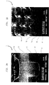
- FIGS. 3A-3B are SEM photographs of a portion of the integrated circuit structure 30 of the present invention.
- the photographs show STI structures which have been filled with HDP-CVD oxide 52 that has been deposited by an inductively coupled plasma source (as described above).
- FIG. 3A concentrates on a single STI of the narrow type, while FIG. 3B depicts an array of such STIs. Notice should be taken of the excellent gapfill of the HDP-CVD oxide layer 52 and the small triangles 54 left above the small active areas 50 on the substrate 40.
- the substrate 40 and narrow trenches 44 are also clearly visible in the photographs.
- the oxide layer is then planarized to expose the active areas.
- the triangular-shaped oxide regions above the STIs allow the CMP step in the planarization scheme to be shortened.
- the purpose of the CMP step is to polish the surface of the substrate to 1) remove the oxide layer in order to expose the active areas, and 2) to obtain a uniform planar topography. Shortening the polishing step reduces oxide erosion in the STI trenches, thereby avoiding unevenness in the surface caused by conventional planarization schemes. In some instances, shortening the CMP step also reduces erosion of the narrow active regions that can occur with an extended CMP step.
- the use of HDP-CVD oxide as a STI fill advantageously enables the height of the oxide in the STI to be substantially determined by the deposition process and not by the CMP removal.
- the duration of the CMP step depends on the time needed to remove the oxide in order to expose the active area. Referring back to Fig. 2B, it is clear that the amount of oxide above the wide active areas 50 is greater than that above narrow active areas 51. As such, the duration of the CMP step is typically based on the time it takes to expose the wide active areas. However, as previously discussed, the time required for the conventional CMP step to expose the wide active areas is generally too long and excessive oxide corrosion in the wide STIs occurs. Also, the CMP step may overpolish the narrow active areas, causing erosion therein. As a result, an unplanar topography is produced.
- the CMP step is shortened to avoid excessive corrosion of the STIs and narrow active regions.
- shortening of the CMP step is achieved by selectively removing portions of the oxide from the triangular-shaped oxide regions above the active areas. By reducing the amount of oxide needed to remove in order to expose the active areas, the corresponding CMP step is shortened.
- the amount of oxide that is removed from the active regions is sufficient to effectively shorten the CMP step so as to expose the active areas without excessive oxide corrosion occurring in the STIs, thus resulting in a substantially planar surface.
- the time needed to remove the amount of oxide in triangles 54 above the narrow active areas 51 is sufficiently short to result in a substantially planar surface in the STIs. As such, the amount of oxide remaining above the wide active regions 50 should not exceed the amount in the triangles 54. If a portion of center if the oxide region 52 is removed, then each of the remaining side portions should not exceed about the amount of oxide in the triangle 54.
- FIGS. 4A-4C show the removal of the portion of the oxide layer from the active areas of integrated device structure 30. Portions of the HDP-CVD oxide layer 52 are removed to expose the active areas 50 and 51. As shown in FIG. 4A, a photoresist layer 60 is formed and patterned over the HDP-CVD oxide layer 52 to expose the active areas. In one embodiment, an inverse active area mask (not shown) is used to form and pattern the HDP-CVD oxide layer. Such a mask is the negative mask of the mask used to form the active areas. Techniques for biasing the inverse mask are well known in the art. Typically, there are overlay inaccuracies associated with the lithograhic process. To compensate for the overlay inaccuracies, the inverse mask is biased. The amount to bias is sufficient to effectively shift the edges of the photoresist onto the sloping edges 55 and 56 of the HDP-CVD oxide layer. The maximum bias allowable depends on the performance of CMP step.
- the bias is between about an amount which is sufficient to effectively shift the edges of the photoresist onto the sloping edges to about an amount which effectively shortens the polishing step so as to expose the active areas with a substantially planar surface.
- the amount of bias is sufficient to shift the edges of the photoresist onto the sloping edges 55 and 56 to about an amount which covers the sloping edges of the oxide layer.
- the triangles 54 would be covered with photoresist (not shown). As a result, only portions of the oxide layer above the wide active areas 50 would be removed.
- the amount of bias is sufficient to effectively shift the mask to cover between about 5-95% of the sloping edges of the oxide layer.
- the amount of bias is sufficient to effectively shift the mask to cover between about 10-90% of the sloping edges of the oxide layer. Even more preferably, the amount of bias is sufficient to shift the mask to effectively cover between about 25-85% of the sloping edges of the oxide layer. Most preferably, the amount of bias is sufficient to shift the mask to effectively cover between about 20-80% of the sloping edges of the oxide layer.
- a mid-ultra violet (MUV) lithography technique can also be used.
- the use of the inverse biased area mask advantageously eliminates the need to randomly generate a new mask in order to expose the active areas.
- the regions of the oxide layer 52 unprotected by photoresist are then etched using a suitable etching technique (such as RIE).
- the RIE etching step is oxide selective.
- oxide selective RIE the silicon substrate and resist act as etch stops.
- the RIE removes only the HDP-CVD oxide layer 52, exposing the semiconductor substrate surface above those areas not covered by the photoresist layer 60.
- the RIE etching process results in the removal of portions of the HDP-CVD oxide layer 52 overlying the active regions. It can also be seen that wedge-shaped portions 62 of the HDP-CVD oxide layer 52 are left on the surfaces of the edges of the active areas after the RIE etching step. These wedge-shaped portions 62 are removed in a subsequent CMP step.
- FIG. 4C the next steps in the integrated circuit planarization scheme are depicted.
- the photoresist mask described above has been removed using an ashing or similar process. These processes are familiar to those skilled in the art and will not be discussed further here.
- the ashing process removes only the photoresist masking layer, leaving the wedge-shaped 62 HDP-CVD oxide portions on the surface of the semiconductor substrate 40.
- the resulting structure is then exposed to a final CMP step which removes all of the remaining HDP-CVD oxide structures 62, leaving a highly planarized topography to the semiconductor substrate 40. Because of the steps taken in the above-described technique regarding the small size of the HDP-CVD oxide structures, this particular CMP step can be kept short, thus minimizing the oxide erosion in the STIs trenches, particularly in the wide STIs trenches.
- the final planarized semiconductor substrate of the integrated circuit structure is depicted.
- the top surface 70 of the semiconductor substrate 40 of the integrated circuit 30 is substantially planar with respect to the top surface of the HDP-CVD oxide-filled shallow trench isolation trenches 72. Since the CMP step is kept short, it is the HDP-CVD oxide deposition process which determines the height of the oxide in the STIs, not the CMP removal step. This is advantageous when compared to prior art processes since it avoids the problem of overpolishing due to extended CMP times which result in the excess erosion of oxide from the STIs.
- the integrated circuit structure 30 of the present invention has been provided with a highly planarized surface structure containing STI regions which permit device isolation, it can then be further processed in accordance with known integrated circuit technology.
- the present invention substantially overcomes many of the problems associated with prior art gapfill and planarization schemes in integrated circuit fabrication processes.
- the HDP-CVD oxide layer deposited by an inductively coupled plasma source provides an insulating oxide layer in the STI regions of the substrate.
- the insulating layer fills these regions without gaps while simultaneously forming triangular-shaped surface structures. Portions of the triangular structures are then removed to shorten the subsequent CMP process.
- the CMP step can be reduced, the problems associated with prior art oxide erosion are substantially avoided.
Applications Claiming Priority (2)
| Application Number | Priority Date | Filing Date | Title |
|---|---|---|---|
| US694072 | 1996-08-08 | ||
| US08/694,072 US5851899A (en) | 1996-08-08 | 1996-08-08 | Gapfill and planarization process for shallow trench isolation |
Publications (2)
| Publication Number | Publication Date |
|---|---|
| EP0825645A1 true EP0825645A1 (de) | 1998-02-25 |
| EP0825645B1 EP0825645B1 (de) | 2007-03-07 |
Family
ID=24787292
Family Applications (1)
| Application Number | Title | Priority Date | Filing Date |
|---|---|---|---|
| EP97306000A Expired - Lifetime EP0825645B1 (de) | 1996-08-08 | 1997-08-07 | Lückenfüllungs- und Planarisierungsverfahren für flache Grabenisolation |
Country Status (7)
| Country | Link |
|---|---|
| US (1) | US5851899A (de) |
| EP (1) | EP0825645B1 (de) |
| JP (1) | JPH1079423A (de) |
| KR (1) | KR100621255B1 (de) |
| CN (1) | CN1099133C (de) |
| DE (1) | DE69737433T2 (de) |
| TW (1) | TW335531B (de) |
Cited By (6)
| Publication number | Priority date | Publication date | Assignee | Title |
|---|---|---|---|---|
| WO1999016124A2 (de) * | 1997-09-22 | 1999-04-01 | Siemens Aktiengesellschaft | Verfahren zur erzeugung von isolationsgräben in einem substrat |
| US6150233A (en) * | 1998-02-13 | 2000-11-21 | Mitsubishi Denki Kabushiki Kaisha | Semiconductor device and method of manufacturing the same |
| DE19829862C2 (de) * | 1998-01-27 | 2001-03-15 | Mitsubishi Electric Corp | Herstellungsverfahren einer Halbleitervorrichtung mit Grabentrennung |
| WO2001056070A1 (en) * | 2000-01-27 | 2001-08-02 | Infineon Technologies North America Corp. | Planarization process to achieve improved uniformity across semiconductor wafers |
| EP1271631A1 (de) * | 2001-06-29 | 2003-01-02 | Interuniversitair Micro-Elektronica Centrum Vzw | Herstellungsverfahren von Halbleiteranordnungen unter Verwendung eines chemisch-mechanischen Polierens |
| CN1314115C (zh) * | 2002-03-15 | 2007-05-02 | 台湾积体电路制造股份有限公司 | 多重金属层内连线结构 |
Families Citing this family (53)
| Publication number | Priority date | Publication date | Assignee | Title |
|---|---|---|---|---|
| JP4195734B2 (ja) * | 1996-06-10 | 2008-12-10 | テキサス インスツルメンツ インコーポレイテツド | 集積回路のトレンチ分離製作方法 |
| US6117345A (en) | 1997-04-02 | 2000-09-12 | United Microelectronics Corp. | High density plasma chemical vapor deposition process |
| TW332915B (en) * | 1997-06-24 | 1998-06-01 | Ti Acer Co Ltd | The producing method for shallow trench isolation with global planarization |
| US6241582B1 (en) * | 1997-09-01 | 2001-06-05 | United Microelectronics Corp. | Chemical mechanical polish machines and fabrication process using the same |
| KR100239453B1 (ko) * | 1997-11-06 | 2000-01-15 | 김영환 | 반도체 소자의 소자 격리층 형성 방법 |
| US6165914A (en) * | 1997-11-12 | 2000-12-26 | Agilent Technologies | Method for fabricating semiconductor devices with thick high quality oxides |
| US6306725B1 (en) * | 1997-11-19 | 2001-10-23 | Texas Instruments Incorporated | In-situ liner for isolation trench side walls and method |
| US6124183A (en) * | 1997-12-18 | 2000-09-26 | Advanced Micro Devices, Inc. | Shallow trench isolation formation with simplified reverse planarization mask |
| US6093611A (en) * | 1997-12-19 | 2000-07-25 | Advanced Micro Devices, Inc. | Oxide liner for high reliability with reduced encroachment of the source/drain region |
| TW498440B (en) * | 1998-03-30 | 2002-08-11 | Hitachi Ltd | Manufacture method of semiconductor device |
| US7001713B2 (en) * | 1998-04-18 | 2006-02-21 | United Microelectronics, Corp. | Method of forming partial reverse active mask |
| US6057210A (en) * | 1998-04-21 | 2000-05-02 | Vanguard International Semiconductor Corporation | Method of making a shallow trench isolation for ULSI formation via in-direct CMP process |
| US6004863A (en) * | 1998-05-06 | 1999-12-21 | Taiwan Semiconductor Manufacturing Company | Non-polishing sacrificial layer etchback planarizing method for forming a planarized aperture fill layer |
| KR100296137B1 (ko) * | 1998-06-16 | 2001-08-07 | 박종섭 | 보호막으로서고밀도플라즈마화학기상증착에의한절연막을갖는반도체소자제조방법 |
| US6013559A (en) * | 1998-07-17 | 2000-01-11 | United Microelectronics Corp. | Method of forming trench isolation |
| JP2000040737A (ja) * | 1998-07-24 | 2000-02-08 | Oki Electric Ind Co Ltd | 素子分離領域の形成方法 |
| TW409344B (en) * | 1998-09-02 | 2000-10-21 | United Microelectronics Corp | Method of producing shallow isolation trench |
| US5930646A (en) * | 1998-10-09 | 1999-07-27 | Chartered Semiconductor Manufacturing, Ltd. | Method of shallow trench isolation |
| US6232043B1 (en) * | 1999-05-25 | 2001-05-15 | Taiwan Semiconductor Manufacturing Company | Rule to determine CMP polish time |
| KR100295917B1 (ko) * | 1999-06-08 | 2001-07-12 | 황인길 | 반도체 소자 분리를 위한 얕은 트렌치 제조 방법 |
| US6319796B1 (en) * | 1999-08-18 | 2001-11-20 | Vlsi Technology, Inc. | Manufacture of an integrated circuit isolation structure |
| DE19939597B4 (de) * | 1999-08-20 | 2006-07-20 | Infineon Technologies Ag | Verfahren zur Herstellung einer mikroelektronischen Struktur mit verbesserter Gatedielektrikahomogenität |
| US6191001B1 (en) * | 1999-08-25 | 2001-02-20 | Lucent Technologies, Inc. | Shallow trench isolation method |
| US7253047B2 (en) | 1999-09-01 | 2007-08-07 | Micron Technology, Inc. | Semiconductor processing methods of forming transistors, semiconductor processing methods of forming dynamic random access memory circuitry, and related integrated circuitry |
| US6356452B1 (en) * | 1999-10-13 | 2002-03-12 | Micron Technology, Inc. | Soldermask opening to prevent delamination |
| US6258676B1 (en) | 1999-11-01 | 2001-07-10 | Chartered Semiconductor Manufacturing Ltd. | Method for forming a shallow trench isolation using HDP silicon oxynitride |
| KR100358054B1 (ko) * | 1999-12-24 | 2002-10-25 | 주식회사 하이닉스반도체 | 반도체 소자의 제조 방법 |
| US6472291B1 (en) | 2000-01-27 | 2002-10-29 | Infineon Technologies North America Corp. | Planarization process to achieve improved uniformity across semiconductor wafers |
| JP3651344B2 (ja) * | 2000-02-03 | 2005-05-25 | セイコーエプソン株式会社 | 半導体装置の製造方法 |
| US6281114B1 (en) * | 2000-02-07 | 2001-08-28 | Infineon Technologies Ag | Planarization after metal chemical mechanical polishing in semiconductor wafer fabrication |
| US6372605B1 (en) * | 2000-06-26 | 2002-04-16 | Agere Systems Guardian Corp. | Additional etching to decrease polishing time for shallow-trench isolation in semiconductor processing |
| US6294423B1 (en) | 2000-11-21 | 2001-09-25 | Infineon Technologies North America Corp. | Method for forming and filling isolation trenches |
| US6667223B2 (en) * | 2001-07-13 | 2003-12-23 | Infineon Technologies Ag | High aspect ratio high density plasma (HDP) oxide gapfill method in a lines and space pattern |
| US6585567B1 (en) | 2001-08-31 | 2003-07-01 | Koninklijke Philips Electronics N.V. | Short CMP polish method |
| US6638145B2 (en) * | 2001-08-31 | 2003-10-28 | Koninklijke Philips Electronics N.V. | Constant pH polish and scrub |
| US6780730B2 (en) | 2002-01-31 | 2004-08-24 | Infineon Technologies Ag | Reduction of negative bias temperature instability in narrow width PMOS using F2 implantation |
| US6673695B1 (en) * | 2002-02-01 | 2004-01-06 | Chartered Semiconductor Manufacturing Ltd. | STI scheme to prevent fox recess during pre-CMP HF dip |
| US6774042B1 (en) * | 2002-02-26 | 2004-08-10 | Taiwan Semiconductor Manufacturing Company | Planarization method for deep sub micron shallow trench isolation process |
| JP2003282438A (ja) * | 2002-03-27 | 2003-10-03 | Seiko Epson Corp | 半導体装置の製造方法及び半導体装置、電気光学装置、電子機器 |
| US6734080B1 (en) * | 2002-05-31 | 2004-05-11 | Advanced Micro Devices, Inc. | Semiconductor isolation material deposition system and method |
| US7164837B2 (en) * | 2002-12-06 | 2007-01-16 | Agency For Science, Technology And Research | Method of fabricating optical waveguide devices with smooth and flat dielectric interfaces |
| US6821865B2 (en) * | 2002-12-30 | 2004-11-23 | Infineon Technologies Ag | Deep isolation trenches |
| JP2004228519A (ja) | 2003-01-27 | 2004-08-12 | Elpida Memory Inc | 半導体装置、及びその製造方法 |
| CN1327503C (zh) * | 2004-09-08 | 2007-07-18 | 上海宏力半导体制造有限公司 | 增进浅槽隔离结构高度均匀性的方法 |
| KR100717823B1 (ko) | 2004-12-28 | 2007-05-11 | 주식회사 하이닉스반도체 | 반도체 소자의 아이엠디막 형성방법 |
| KR100645211B1 (ko) * | 2005-07-28 | 2006-11-10 | 동부일렉트로닉스 주식회사 | 플래시 메모리 셀의 플로팅 게이트 형성 방법 |
| KR100972904B1 (ko) * | 2008-05-16 | 2010-07-28 | 주식회사 하이닉스반도체 | 반도체 소자의 형성 방법 |
| DE102010046213B3 (de) * | 2010-09-21 | 2012-02-09 | Infineon Technologies Austria Ag | Verfahren zur Herstellung eines Strukturelements und Halbleiterbauelement mit einem Strukturelement |
| JP5447722B1 (ja) * | 2013-07-17 | 2014-03-19 | 富士ゼロックス株式会社 | 情報処理システム及びプログラム |
| US9773682B1 (en) * | 2016-07-05 | 2017-09-26 | United Microelectronics Corp. | Method of planarizing substrate surface |
| KR102614427B1 (ko) | 2018-09-19 | 2023-12-18 | 삼성전자주식회사 | 반도체 소자 및 그 형성 방법 |
| TWI756003B (zh) | 2021-01-04 | 2022-02-21 | 力晶積成電子製造股份有限公司 | 平坦化方法 |
| CN113471138B (zh) * | 2021-07-05 | 2023-10-24 | 长鑫存储技术有限公司 | 半导体基底的制备方法及半导体器件 |
Citations (4)
| Publication number | Priority date | Publication date | Assignee | Title |
|---|---|---|---|---|
| EP0407047A2 (de) * | 1989-07-03 | 1991-01-09 | Advanced Micro Devices, Inc. | Verfahren zum Ebnen von Topologien für integrierte Schaltungen |
| EP0545263A2 (de) * | 1991-11-29 | 1993-06-09 | Sony Corporation | Verfahren zur Herstellung einer Isolationsprobe mittels einer Polierschritt |
| JPH05335291A (ja) * | 1991-10-04 | 1993-12-17 | Sony Corp | 半導体装置の製造方法 |
| EP0697722A2 (de) * | 1994-08-17 | 1996-02-21 | Texas Instruments Incorporated | Verfahren zur Planarizierung von Dielektriken über Halbleitervorrichtungen |
Family Cites Families (10)
| Publication number | Priority date | Publication date | Assignee | Title |
|---|---|---|---|---|
| US4665007A (en) * | 1985-08-19 | 1987-05-12 | International Business Machines Corporation | Planarization process for organic filling of deep trenches |
| US4962064A (en) * | 1988-05-12 | 1990-10-09 | Advanced Micro Devices, Inc. | Method of planarization of topologies in integrated circuit structures |
| JP2870054B2 (ja) * | 1989-10-25 | 1999-03-10 | ソニー株式会社 | 半導体装置の製造方法 |
| US5187119A (en) * | 1991-02-11 | 1993-02-16 | The Boeing Company | Multichip module and integrated circuit substrates having planarized patterned surfaces |
| US5245213A (en) * | 1991-10-10 | 1993-09-14 | Sgs-Thomson Microelectronics, Inc. | Planarized semiconductor product |
| US5292689A (en) * | 1992-09-04 | 1994-03-08 | International Business Machines Corporation | Method for planarizing semiconductor structure using subminimum features |
| US5494857A (en) * | 1993-07-28 | 1996-02-27 | Digital Equipment Corporation | Chemical mechanical planarization of shallow trenches in semiconductor substrates |
| US5387540A (en) * | 1993-09-30 | 1995-02-07 | Motorola Inc. | Method of forming trench isolation structure in an integrated circuit |
| US5399533A (en) * | 1993-12-01 | 1995-03-21 | Vlsi Technology, Inc. | Method improving integrated circuit planarization during etchback |
| US5385861A (en) * | 1994-03-15 | 1995-01-31 | National Semiconductor Corporation | Planarized trench and field oxide and poly isolation scheme |
-
1996
- 1996-08-08 US US08/694,072 patent/US5851899A/en not_active Expired - Lifetime
-
1997
- 1997-08-07 DE DE69737433T patent/DE69737433T2/de not_active Expired - Lifetime
- 1997-08-07 TW TW086111321A patent/TW335531B/zh not_active IP Right Cessation
- 1997-08-07 EP EP97306000A patent/EP0825645B1/de not_active Expired - Lifetime
- 1997-08-08 KR KR1019970037940A patent/KR100621255B1/ko not_active IP Right Cessation
- 1997-08-08 CN CN97116168A patent/CN1099133C/zh not_active Expired - Lifetime
- 1997-08-08 JP JP9225570A patent/JPH1079423A/ja not_active Withdrawn
Patent Citations (4)
| Publication number | Priority date | Publication date | Assignee | Title |
|---|---|---|---|---|
| EP0407047A2 (de) * | 1989-07-03 | 1991-01-09 | Advanced Micro Devices, Inc. | Verfahren zum Ebnen von Topologien für integrierte Schaltungen |
| JPH05335291A (ja) * | 1991-10-04 | 1993-12-17 | Sony Corp | 半導体装置の製造方法 |
| EP0545263A2 (de) * | 1991-11-29 | 1993-06-09 | Sony Corporation | Verfahren zur Herstellung einer Isolationsprobe mittels einer Polierschritt |
| EP0697722A2 (de) * | 1994-08-17 | 1996-02-21 | Texas Instruments Incorporated | Verfahren zur Planarizierung von Dielektriken über Halbleitervorrichtungen |
Non-Patent Citations (2)
| Title |
|---|
| CHATTERJEE A ET AL: "A shallow trench isolation study for 0.25/0.18 mu m CMOS technologies and beyond", 1996 SYMPOSIUM ON VLSI TECHNOLOGY. DIGEST OF TECHNICAL PAPERS (IEEE CAT. NO.96CH35944), 1996 SYMPOSIUM ON VLSI TECHNOLOGY. DIGEST OF TECHNICAL PAPERS, HONOLULU, HI, USA, 11-13 JUNE 1996, ISBN 0-7803-3342-X, 1996, GAITHERSBURG, MD, USA, WIDERKEHR & ASSOCIATES, USA, pages 156 - 157, XP002047837 * |
| PATENT ABSTRACTS OF JAPAN vol. 018, no. 158 (E - 1525) 16 March 1994 (1994-03-16) * |
Cited By (10)
| Publication number | Priority date | Publication date | Assignee | Title |
|---|---|---|---|---|
| WO1999016124A2 (de) * | 1997-09-22 | 1999-04-01 | Siemens Aktiengesellschaft | Verfahren zur erzeugung von isolationsgräben in einem substrat |
| WO1999016124A3 (de) * | 1997-09-22 | 1999-05-20 | Siemens Ag | Verfahren zur erzeugung von isolationsgräben in einem substrat |
| DE19829862C2 (de) * | 1998-01-27 | 2001-03-15 | Mitsubishi Electric Corp | Herstellungsverfahren einer Halbleitervorrichtung mit Grabentrennung |
| US6323102B1 (en) | 1998-01-27 | 2001-11-27 | Mitsubishi Denki Kabushiki Kaisha | Method of manufacturing a semiconductor device |
| US6150233A (en) * | 1998-02-13 | 2000-11-21 | Mitsubishi Denki Kabushiki Kaisha | Semiconductor device and method of manufacturing the same |
| DE19843160B4 (de) * | 1998-02-13 | 2005-05-12 | Mitsubishi Denki K.K. | Halbleitervorrichtung mit Grabentrennung und Verfahren zu dessen Herstellung mittels Vorplanarisierung |
| WO2001056070A1 (en) * | 2000-01-27 | 2001-08-02 | Infineon Technologies North America Corp. | Planarization process to achieve improved uniformity across semiconductor wafers |
| EP1271631A1 (de) * | 2001-06-29 | 2003-01-02 | Interuniversitair Micro-Elektronica Centrum Vzw | Herstellungsverfahren von Halbleiteranordnungen unter Verwendung eines chemisch-mechanischen Polierens |
| US7033941B2 (en) | 2001-06-29 | 2006-04-25 | Interuniversitair Microelektronica Centrum (Imec) | Method of producing semiconductor devices using chemical mechanical polishing |
| CN1314115C (zh) * | 2002-03-15 | 2007-05-02 | 台湾积体电路制造股份有限公司 | 多重金属层内连线结构 |
Also Published As
| Publication number | Publication date |
|---|---|
| CN1176488A (zh) | 1998-03-18 |
| DE69737433T2 (de) | 2007-11-29 |
| KR19980018523A (ko) | 1998-06-05 |
| JPH1079423A (ja) | 1998-03-24 |
| CN1099133C (zh) | 2003-01-15 |
| US5851899A (en) | 1998-12-22 |
| KR100621255B1 (ko) | 2006-12-04 |
| DE69737433D1 (de) | 2007-04-19 |
| TW335531B (en) | 1998-07-01 |
| EP0825645B1 (de) | 2007-03-07 |
Similar Documents
| Publication | Publication Date | Title |
|---|---|---|
| US5851899A (en) | Gapfill and planarization process for shallow trench isolation | |
| US6169012B1 (en) | Chemical mechanical polishing for forming a shallow trench isolation structure | |
| KR100428805B1 (ko) | 트렌치 소자분리 구조체 및 그 형성 방법 | |
| US6805614B2 (en) | Multilayered CMP stop for flat planarization | |
| US5492858A (en) | Shallow trench isolation process for high aspect ratio trenches | |
| JPH05206261A (ja) | 集積回路製造において溝分離を行うための平坦化方法 | |
| US6057207A (en) | Shallow trench isolation process using chemical-mechanical polish with self-aligned nitride mask on HDP-oxide | |
| JPH09107028A (ja) | 半導体装置の素子分離方法 | |
| US6165869A (en) | Method to avoid dishing in forming trenches for shallow trench isolation | |
| WO1997039479A1 (en) | Method for forming semiconductor field region dielectrics having globally planarized upper surfaces | |
| US6103581A (en) | Method for producing shallow trench isolation structure | |
| US7001713B2 (en) | Method of forming partial reverse active mask | |
| KR100979230B1 (ko) | 반도체 소자의 얕은 트랜치 소자분리막 형성방법 | |
| US6897121B2 (en) | Method of removing HDP oxide deposition | |
| KR100742961B1 (ko) | 반도체 소자의 평탄화 방법 | |
| KR100583508B1 (ko) | 집적 회로 웨이퍼 평탄화 방법 | |
| US6991993B2 (en) | Method of fabricating trench isolation structure of a semiconductor device | |
| KR20040038145A (ko) | 반도체 소자의 소자분리막 형성방법 | |
| KR100712983B1 (ko) | 반도체 소자의 평탄화 방법 | |
| KR100190065B1 (ko) | 트렌치 소자분리방법 | |
| JP2003152073A (ja) | 半導体装置の製造方法 | |
| KR20000019159A (ko) | 반도체 소자 분리를 위한 트랜치 제조 방법 | |
| KR20050006510A (ko) | 반도체소자의 소자분리막 평탄화 방법 | |
| KR20010059029A (ko) | 반도체소자의 소자분리막 형성방법 | |
| JPH07297274A (ja) | 半導体装置の製造方法 |
Legal Events
| Date | Code | Title | Description |
|---|---|---|---|
| PUAI | Public reference made under article 153(3) epc to a published international application that has entered the european phase |
Free format text: ORIGINAL CODE: 0009012 |
|
| AK | Designated contracting states |
Kind code of ref document: A1 Designated state(s): DE FR GB IT |
|
| AX | Request for extension of the european patent |
Free format text: AL;LT;LV;RO;SI |
|
| 17P | Request for examination filed |
Effective date: 19980818 |
|
| AKX | Designation fees paid |
Free format text: DE FR GB IT |
|
| RBV | Designated contracting states (corrected) |
Designated state(s): DE FR GB IT |
|
| 17Q | First examination report despatched |
Effective date: 20040220 |
|
| RAP1 | Party data changed (applicant data changed or rights of an application transferred) |
Owner name: INFINEON TECHNOLOGIES AG |
|
| GRAP | Despatch of communication of intention to grant a patent |
Free format text: ORIGINAL CODE: EPIDOSNIGR1 |
|
| GRAS | Grant fee paid |
Free format text: ORIGINAL CODE: EPIDOSNIGR3 |
|
| GRAA | (expected) grant |
Free format text: ORIGINAL CODE: 0009210 |
|
| AK | Designated contracting states |
Kind code of ref document: B1 Designated state(s): DE FR GB IT |
|
| REG | Reference to a national code |
Ref country code: GB Ref legal event code: FG4D |
|
| REF | Corresponds to: |
Ref document number: 69737433 Country of ref document: DE Date of ref document: 20070419 Kind code of ref document: P |
|
| RAP2 | Party data changed (patent owner data changed or rights of a patent transferred) |
Owner name: QIMONDA AG |
|
| REG | Reference to a national code |
Ref country code: FR Ref legal event code: TP |
|
| PLBE | No opposition filed within time limit |
Free format text: ORIGINAL CODE: 0009261 |
|
| STAA | Information on the status of an ep patent application or granted ep patent |
Free format text: STATUS: NO OPPOSITION FILED WITHIN TIME LIMIT |
|
| 26N | No opposition filed |
Effective date: 20071210 |
|
| REG | Reference to a national code |
Ref country code: DE Ref legal event code: R081 Ref document number: 69737433 Country of ref document: DE Owner name: POLARIS INNOVATIONS LTD., IE Free format text: FORMER OWNER: QIMONDA AG, 81739 MUENCHEN, DE Ref country code: DE Ref legal event code: R081 Ref document number: 69737433 Country of ref document: DE Owner name: INFINEON TECHNOLOGIES AG, DE Free format text: FORMER OWNER: QIMONDA AG, 81739 MUENCHEN, DE |
|
| REG | Reference to a national code |
Ref country code: FR Ref legal event code: PLFP Year of fee payment: 19 |
|
| REG | Reference to a national code |
Ref country code: DE Ref legal event code: R081 Ref document number: 69737433 Country of ref document: DE Owner name: POLARIS INNOVATIONS LTD., IE Free format text: FORMER OWNER: INFINEON TECHNOLOGIES AG, 85579 NEUBIBERG, DE |
|
| REG | Reference to a national code |
Ref country code: FR Ref legal event code: TP Owner name: INFINEON TECHNOLOGIES AG, DE Effective date: 20160212 |
|
| REG | Reference to a national code |
Ref country code: FR Ref legal event code: PLFP Year of fee payment: 20 |
|
| PGFP | Annual fee paid to national office [announced via postgrant information from national office to epo] |
Ref country code: DE Payment date: 20160802 Year of fee payment: 20 Ref country code: GB Payment date: 20160803 Year of fee payment: 20 Ref country code: IT Payment date: 20160822 Year of fee payment: 20 |
|
| PGFP | Annual fee paid to national office [announced via postgrant information from national office to epo] |
Ref country code: FR Payment date: 20160712 Year of fee payment: 20 |
|
| REG | Reference to a national code |
Ref country code: DE Ref legal event code: R071 Ref document number: 69737433 Country of ref document: DE |
|
| REG | Reference to a national code |
Ref country code: GB Ref legal event code: PE20 Expiry date: 20170806 |
|
| PG25 | Lapsed in a contracting state [announced via postgrant information from national office to epo] |
Ref country code: GB Free format text: LAPSE BECAUSE OF EXPIRATION OF PROTECTION Effective date: 20170806 |