EP0820103B1 - Cellule Flash EEPROM à un seul niveau de polysilicium et méthode pour sa fabrication - Google Patents
Cellule Flash EEPROM à un seul niveau de polysilicium et méthode pour sa fabrication Download PDFInfo
- Publication number
- EP0820103B1 EP0820103B1 EP96830398A EP96830398A EP0820103B1 EP 0820103 B1 EP0820103 B1 EP 0820103B1 EP 96830398 A EP96830398 A EP 96830398A EP 96830398 A EP96830398 A EP 96830398A EP 0820103 B1 EP0820103 B1 EP 0820103B1
- Authority
- EP
- European Patent Office
- Prior art keywords
- region
- oxide layer
- cell
- active area
- flash eeprom
- Prior art date
- Legal status (The legal status is an assumption and is not a legal conclusion. Google has not performed a legal analysis and makes no representation as to the accuracy of the status listed.)
- Expired - Lifetime
Links
- 238000004519 manufacturing process Methods 0.000 title claims description 21
- 229910021420 polycrystalline silicon Inorganic materials 0.000 title claims description 19
- 229920005591 polysilicon Polymers 0.000 title claims description 19
- 238000000034 method Methods 0.000 claims description 20
- 239000004065 semiconductor Substances 0.000 claims description 11
- 239000002784 hot electron Substances 0.000 claims description 3
- 230000005689 Fowler Nordheim tunneling Effects 0.000 claims description 2
- 238000002347 injection Methods 0.000 claims description 2
- 239000007924 injection Substances 0.000 claims description 2
- 239000000463 material Substances 0.000 claims 2
- 239000007943 implant Substances 0.000 description 22
- 239000003990 capacitor Substances 0.000 description 13
- 230000015572 biosynthetic process Effects 0.000 description 12
- 238000009792 diffusion process Methods 0.000 description 12
- 239000000758 substrate Substances 0.000 description 9
- OAICVXFJPJFONN-UHFFFAOYSA-N Phosphorus Chemical compound [P] OAICVXFJPJFONN-UHFFFAOYSA-N 0.000 description 7
- 229910052698 phosphorus Inorganic materials 0.000 description 7
- 239000011574 phosphorus Substances 0.000 description 7
- 229910052785 arsenic Inorganic materials 0.000 description 6
- RQNWIZPPADIBDY-UHFFFAOYSA-N arsenic atom Chemical compound [As] RQNWIZPPADIBDY-UHFFFAOYSA-N 0.000 description 6
- 239000002019 doping agent Substances 0.000 description 6
- 238000005530 etching Methods 0.000 description 4
- 230000010354 integration Effects 0.000 description 3
- 230000008878 coupling Effects 0.000 description 2
- 238000010168 coupling process Methods 0.000 description 2
- 238000005859 coupling reaction Methods 0.000 description 2
- 230000000694 effects Effects 0.000 description 2
- 238000002513 implantation Methods 0.000 description 2
- 125000006850 spacer group Chemical group 0.000 description 2
- 230000002411 adverse Effects 0.000 description 1
- 239000002800 charge carrier Substances 0.000 description 1
- 230000008021 deposition Effects 0.000 description 1
- 230000005669 field effect Effects 0.000 description 1
- 239000011810 insulating material Substances 0.000 description 1
- 238000004806 packaging method and process Methods 0.000 description 1
- 230000005641 tunneling Effects 0.000 description 1
Images


Classifications
-
- H—ELECTRICITY
- H01—ELECTRIC ELEMENTS
- H01L—SEMICONDUCTOR DEVICES NOT COVERED BY CLASS H10
- H01L29/00—Semiconductor devices adapted for rectifying, amplifying, oscillating or switching, or capacitors or resistors with at least one potential-jump barrier or surface barrier, e.g. PN junction depletion layer or carrier concentration layer; Details of semiconductor bodies or of electrodes thereof ; Multistep manufacturing processes therefor
- H01L29/66—Types of semiconductor device ; Multistep manufacturing processes therefor
- H01L29/66007—Multistep manufacturing processes
- H01L29/66075—Multistep manufacturing processes of devices having semiconductor bodies comprising group 14 or group 13/15 materials
- H01L29/66227—Multistep manufacturing processes of devices having semiconductor bodies comprising group 14 or group 13/15 materials the devices being controllable only by the electric current supplied or the electric potential applied, to an electrode which does not carry the current to be rectified, amplified or switched, e.g. three-terminal devices
- H01L29/66409—Unipolar field-effect transistors
- H01L29/66477—Unipolar field-effect transistors with an insulated gate, i.e. MISFET
- H01L29/66825—Unipolar field-effect transistors with an insulated gate, i.e. MISFET with a floating gate
-
- H—ELECTRICITY
- H01—ELECTRIC ELEMENTS
- H01L—SEMICONDUCTOR DEVICES NOT COVERED BY CLASS H10
- H01L29/00—Semiconductor devices adapted for rectifying, amplifying, oscillating or switching, or capacitors or resistors with at least one potential-jump barrier or surface barrier, e.g. PN junction depletion layer or carrier concentration layer; Details of semiconductor bodies or of electrodes thereof ; Multistep manufacturing processes therefor
- H01L29/66—Types of semiconductor device ; Multistep manufacturing processes therefor
- H01L29/68—Types of semiconductor device ; Multistep manufacturing processes therefor controllable by only the electric current supplied, or only the electric potential applied, to an electrode which does not carry the current to be rectified, amplified or switched
- H01L29/76—Unipolar devices, e.g. field effect transistors
- H01L29/772—Field effect transistors
- H01L29/78—Field effect transistors with field effect produced by an insulated gate
- H01L29/788—Field effect transistors with field effect produced by an insulated gate with floating gate
- H01L29/7881—Programmable transistors with only two possible levels of programmation
- H01L29/7884—Programmable transistors with only two possible levels of programmation charging by hot carrier injection
- H01L29/7885—Hot carrier injection from the channel
Definitions
- the present invention relates to a single polysilicon level flash EEPROM cell, and to a manufacturing process for obtaining the same.
- a flash EEPROM cell is a memory cell that can be electrically programmed arid electrically erased.
- the cell comprises source and drain electrodes, a floating gate and a control gate.
- Programmation of the memory cell involves injection of hot electrons from the drain electrode into the floating gate, where the electrons get trapped. Erasure is achieved by means of Fowler-Nordheim tunneling of electrons from the floating gate normally to the source electrode.
- Conventional flash EEPROM cells are stacked-gate devices wherein the floating gate is formed of a first level of polysilicon isolated from the semiconductor substrate by means of an oxide layer, and the control gate is formed of a second level of polysilicon isolated from the floating gate by means of a dielectric layer.
- the patent application EP 471 131 discloses an process for obtaining an N-channel single polysilicon level EPROM cell.
- the patent application EP 120 303 discloses an EEPROM which has a high packaging density and which is not liable to any adverse effects from change in a manufacturing process.
- the patent US 4,019,197 discloses a storage device having a field effect transistor with a floating insulating gate electrode on which information containing charge can be stored by tunnelling charge carriers between the semiconductor body and the gate electrode. In particular it discloses an EEPROM cell.
- the flash EEPROM cell of the present invention can be fabricated by means of a process as defined in claim 4.
- the flash EEPROM memory cell according to the present invention has a single polysilicon level; thanks to this, it is simpler and cheaper to be fabricated. In fact, it can be fabricated by means of conventional CMOS processes with the addition of only a few dedicated masks. For example, in CMOS processes providing for the integration of capacitors, the source and drain regions and the control gate region of the cell can be formed by means of the same implant used to form the capacitors.
- the formation of the floating gate of the cell can be accomplished simultaneously with the formation of gates of MOS transistors: if the thickness of the oxide layer which insulates the gate of the MOS transistors from their channels is sufficiently low, said oxide layer can also form the tunnel oxide layer for the flash EEPROM cell, otherwise a single additional mask is necessary to form the tunnel oxide layer for the cell.
- the formation of the control gate region of the cell can be obtained using the same implant step provided in all CMOS processes for the formation of well regions in the substrate for the integration of MOS transistors, and the formation of the source and drain regions of the cell can be achieved by means of a dedicated masked implant; in this case, even if a further additional mask is necessary, the performances of the memory cell can be improved.
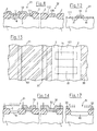
- the flash EEPROM cell which in this example is assumed to be of the N channel type, comprises N type source and drain regions 71, 72 and 81, 82 formed in a P type semiconductor substrate 1 in a first active area region 33 delimited by thick field oxide layer portions 2, an N type control gate diffusion 9 formed in substrate 1 in a second active area region 34 substantially parallel to the first active area region 33, a gate oxide layer 11 covering the second active area region 34 and a tunnel oxide layer 111, usually thinner than the gate oxide layer 11, covering the first active area region 33.
- a polysilicon floating gate 10 extends transversally to the first and second active area regions 33, 34; in the second active area region 34 the polysilicon floating gate 10 is isolated from the control gate diffusion 9 by means of the gate oxide Layer 11; in the first active area region 33 the polysilicon floating gate 10 is isolated from the substrate 1 and from the source and drain regions 71 and 81 by means of the tunnel oxide layer 111.
- the N-channel MOSFET is similarly formed in a respective active area region 35 also delimited by thick field oxide layer portions 2, wherein N type source and drain regions 37 and 38 are formed in substrate 1; a gate oxide layer 112 covers the substrate 1 and a polysilicon gate 100 is disposed over the gate oxide layer 112.
- the flash EEPROM memory cell of the present invention is not a stacked-gate device, because the control gate is not superimposed over the floating gate.
- conventional flash EEPROM cells are double polysilicon Level devices
- the flash EEPROM cell of the present invention is a single polysilicon Level device.
- the operation of the single polysilicon level cell of the present invention is similar to that of conventional flash EEPROM cells: in write mode, a voltage of 8 to 12 V is applied to the control gate diffusion, a voltage of 3 to 5 V is applied to the drain region and the source region is kept grounded; hot electrons generated in the channel region of the memory cell (the region of substrate 1 comprised between the source and drain regions) are injected into the floating gate 10, where they get trapped; in erase mode, the control gate is kept grounded, the drain region is left floating and a voltage of 8 to 12 V is applied to the source region; electrons trapped in the floating gate 10 tunnel (Fowler-Nordheim tunnel effect) through the tunnel oxide layer into the source region. In read mode, a voltage of approximately 5 V is applied to the control gate, the drain region is biased at approximately 1 V and the source region is kept grounded.
- a field oxide Layer 2 is selectively formed over substrate 1, for example by means of the known LOCOS technique.
- field oxide Layer 2 is not formed over the active area regions 33 and 34; similarly, in region 32 field oxide layer 2 is not formed over active area region 35 (Fig. 4).
- This implant, with these doses, can be normally provided in conventional CMOS processes in order to create capacitors; in this case, no additional mask is necessary. If instead no capacitors are to be formed in the chip, a dedicated mask is required.
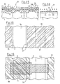
- a gate oxide layer 11, 101, 112 with thickness of, normally, 200 Angstroms is grown over the active area regions 33, 34 and 35, respectively (Figs. 6 and 10).
- a resist mask 50 is then formed which leaves uncovered only the active area region 33 (Fig. 13).
- the gate oxide layer 101 in region 33 is then removed (Figs. 7 and 11), and a thinner tunnel oxide layer 111 is subsequently formed over active area region 33, the tunnel oxide layer haying a thickness of approximately 80 to 140 Angstroms.
- a polyslicon layer is then deposited and selectively removed to define the floating gate 10 of the flash EEPROM cell and the gate 100 of MOSFET 32.
- N type dopant preferably phosphorus
- An N type dopant is then implanted in a dose of approximately 1E13 to 5E13 atoms/cm 2 in the active area region 33 to form regions 72 and 82 of source and drain of the memory cell aligned with the floating gate of the cell; by means of this same implant, in the area of transistor 32 the source and drain regions 37 and 38 are created.
- Insulating material spacers 12, 13 and 39, 40 are then formed at the sides of the polysilicon floating gate 10 of the memory cell as well as at the sides of the polysilicon gate 100 of transistor 32.
- the memory cell and the transistor are then implanted with an N type dopant, preferably arsenic in a dose of approximately 1E15 to 5E15 atoms/cm 2 , in a self aligned manner with the spacers 12, 13 and 39, 40.
- an N type dopant preferably arsenic in a dose of approximately 1E15 to 5E15 atoms/cm 2 , in a self aligned manner with the spacers 12, 13 and 39, 40.
- the process of the present invention requires at most two additional mask, i.e. the one for the dopant implantation for creating the control gate diffusion 9 and the source and drain regions 71 and 81 of the cell, and the one for the removal of the gate oxide layer 101 where the tunnel oxide Layer is to be formed.
- control gate diffusion and the source and drain regions of the memory cells can be formed by means of the implant step used to create capacitors, so that in this case only one additional mask is necessary for the fabrication of the memory cell.
- the mask for the selective etching of the gate oxide layer is already provided in the manufacturing process for the definition of tunnel oxide areas of the EEPROM cells; in this case, no additional masks at all are required.
- the thickness of the gate oxide layers of the MOS transistors will be lower than the current 200 Angstroms; in particular, the gate oxide layers could have a thickness approximately equal to that of the tunnel oxide layers.
- the manufacturing process previously described it would not be necessary to selectively etch the gate oxide layer to form the tunnel oxide layer, so that one more mask could be eliminated.
- no additional masks at all would be necessary to form the flash EEPROM cell of the present invention.
- the control gate diffusion 9 is formed by means of a masked implant of an N type dopant, preferably phosphorus, in a dose of approximately 5E12 to 2E13 atoms/cm 2 .
- an N type dopant preferably phosphorus
- Such an implant is conventionally provided in CMOS manufacturing processes for the creation of N type well regions 90 (Fig. 17) wherein the P-channel MOSFETs are to be integrated.
- This implant due to the low implant dose, is not suitable for forming also the source and drain regions of the flash EEPROM cell, so the active area region 33 shall be masked by means of a resist mask 55 (Fig. 18); also the region 32 of the N channel MOSFET is to be masked (Fig. 14).
- a resist mask 56 is formed (Figs. 15 and 19) and an implant of N type dopants, preferably arsenic plus phosphorus in respective doses of 1E15 to 5E15 atoms/cm 2 and 5E13 to 5E14 atoms/cm 2 and at respective energies of 20 to 50 KeV and 30 to 100 KeV, is performed to form source and drain regions 73 and 83 of the memory cell.
- N type dopants preferably arsenic plus phosphorus in respective doses of 1E15 to 5E15 atoms/cm 2 and 5E13 to 5E14 atoms/cm 2 and at respective energies of 20 to 50 KeV and 30 to 100 KeV
- the memory cell fabricated according to the second embodiment of manufacturing process has better performances; in fact, the dedicated arsenic and phosphorus implant used to form the source and drain regions of the memory cell allows to reduce the current related to band-to-band tunneling (BBT) during electrical erasure of the memory cell.
- BBT band-to-band tunneling
- the manufacturing process provides, as in the first embodiment, for forming the control gate diffusion 9 of the memory cell exploiting the implant that can be provided in a CMOS process for the creation of capacitors.
- the source and drain regions of the memory cell are not formed by means of this implant simultaneously with the control gate diffusion.
- the source and drain regions of the memory cell are instead formed in the same way as in the second embodiment, i.e. by means of a dedicated implant of arsenic and phosphorus.
- the third embodiment allows for a reduction of the area occupied by the memory cell: in fact, since the implant dose used to form capacitors is generally higher than that used to create N type wells, the doping Level of the control gate diffusion is higher; this allows to achieve a higher capacitive coupling between the control gate diffusion and the floating gate even if the area of superposition between the former and the latter is reduced.
- the number of additional masks with respect to a conventional CMOS process is at most three, i.e. the mask for the formation of the control gate diffusion of the memory cell (in the case the CMOS process does not already provide for the formation of capacitors), the mask for the selective etching of the gate oxide Layer over the channel region of the memory cell, and the mask for the dedicated implant of arsenic and phosphorus for the formation of the source and drain regions of the memory cell.
- the CMOS process already provides for the formation of capacitors, only two additional masks are required.
Claims (4)
- Cellule EEPROM flash comportant des régions source et drain semiconductrices (71, 72, 81, 82 ; 73, 83) d'un premier type de conductivité formées dans une première région d'aire active (33) d'une couche de matière semiconductrice (1) d'un deuxième type de conductivité et écartées l'une de l'autre dans une première direction de façon à définir une région de canal entre elles, une grille flottante (10) et une grille de commande (9), où la cellule est programmable par injection d'électrons chauds en provenance de la région de drain (81, 82 ; 83) dans la grille flottante (10) et est effacable par effet tunnel de Fowler-Nordheim d'électrons, de la grille flottante (10) à la région de source (71, 72 ; 73) ;
caractérisée en ce que :la grille de commande (9) comprend une troisième région semiconductrice dopée du premier type de conductivité formée dans une deuxième région d'aire active (34) de la couche de matière semiconductrice (1) ;la grille flottante (10) comprend une bande de silicium polycristallin s'étendant suivant une deuxième direction sensiblement perpendiculaire à la première direction sur la région de canal et la grille de commande et étant isolée respectivement de celle-ci par une première couche d'oxyde (111) possédant une première épaisseur et par une deuxième couche d'oxyde (11) possédant une deuxième épaisseur ;ladite première épaisseur est comprise entre 8 et 14 nm et ladite deuxième épaisseur est d'environ 20 nm. - Cellule EEPROM flash selon la revendication 1, caractérisée ce que lesdites première et deuxième régions d'aire actives (33, 34) sont délimitées par des parties (2) de couches d'oxyde de champ.
- Cellule EEPROM flash selon l'une quelconque des revendications précédentes, caractérisée en ce que ledit premier type de conductivité est le type N et ledit deuxième type de conductivité est le type P.
- Procédé de fabrication d'une cellule EEPROM définie selon l'une quelconque des revendications précédentes, comprenant la succession suivante d'opérations :former dans une couche semiconductrice (1) d'un premier type de conductivité des première et deuxième régions d'aire actives (33, 34) délimitées par des parties (2) de couches d'oxyde de champ ;former dans ladite première région d'aire active (33) des première et deuxième régions semiconductrices dopées (71, 72, 81, 82 ; 73, 83) d'un deuxième type de conductivité constituant des régions de source et de drain de la cellule écartées l'une de l'autre dans une première direction et définissant une région de canal entre elles et formant dans ladite deuxième région d'aire active (34) une troisième région semiconductrice dopée (9) du deuxième type de conductivité constituant une grille de commande de la cellule ;faire croítre une couche d'oxyde de grille plus épaisse (11) ayant une épaisseur d'environ 20 nm sur la région de grille de commande (9) ;faire croítre une couche d'oxyde tunnel plus mince (111) ayant une épaisseur comprise entre 8 et 14 nm sur la région de canal ;former sur lesdites couches d'oxyde (11, 111) une bande de silicium polycristallin (10) qui s'étend dans une deuxième direction sensiblement perpendiculaire à la première direction et qui constitue une grille flottante (9) de la cellule.
Priority Applications (5)
| Application Number | Priority Date | Filing Date | Title |
|---|---|---|---|
| DE69624107T DE69624107T2 (de) | 1996-07-18 | 1996-07-18 | Flash-EEPROM-Zelle mit einziger Polysiliziumschicht und Verfahren zur Herstellung |
| EP96830398A EP0820103B1 (fr) | 1996-07-18 | 1996-07-18 | Cellule Flash EEPROM à un seul niveau de polysilicium et méthode pour sa fabrication |
| US08/883,405 US5936276A (en) | 1996-07-18 | 1997-06-26 | Single polysilicon level flash EEPROM cell and manufacturing process therefor |
| JP9191226A JPH1070204A (ja) | 1996-07-18 | 1997-07-16 | フラッシュeepromメモリセル及びその製造方法 |
| US09/328,033 US6355523B1 (en) | 1996-07-18 | 1999-06-08 | Manufacturing process for making single polysilicon level flash EEPROM cell |
Applications Claiming Priority (1)
| Application Number | Priority Date | Filing Date | Title |
|---|---|---|---|
| EP96830398A EP0820103B1 (fr) | 1996-07-18 | 1996-07-18 | Cellule Flash EEPROM à un seul niveau de polysilicium et méthode pour sa fabrication |
Publications (2)
| Publication Number | Publication Date |
|---|---|
| EP0820103A1 EP0820103A1 (fr) | 1998-01-21 |
| EP0820103B1 true EP0820103B1 (fr) | 2002-10-02 |
Family
ID=8225963
Family Applications (1)
| Application Number | Title | Priority Date | Filing Date |
|---|---|---|---|
| EP96830398A Expired - Lifetime EP0820103B1 (fr) | 1996-07-18 | 1996-07-18 | Cellule Flash EEPROM à un seul niveau de polysilicium et méthode pour sa fabrication |
Country Status (4)
| Country | Link |
|---|---|
| US (2) | US5936276A (fr) |
| EP (1) | EP0820103B1 (fr) |
| JP (1) | JPH1070204A (fr) |
| DE (1) | DE69624107T2 (fr) |
Families Citing this family (14)
| Publication number | Priority date | Publication date | Assignee | Title |
|---|---|---|---|---|
| WO2000060672A1 (fr) * | 1999-03-31 | 2000-10-12 | Koninklijke Philips Electronics N.V. | Dispositif semi-conducteur comprenant une cellule memoire non volatile |
| EP1091408A1 (fr) | 1999-10-07 | 2001-04-11 | STMicroelectronics S.r.l. | Cellule mémoire non-volatile avec un niveau unique de polysilicium |
| EP1096575A1 (fr) * | 1999-10-07 | 2001-05-02 | STMicroelectronics S.r.l. | Cellule de mémoire rémanente à un seul niveau de polysilicium et méthode pour sa fabrication |
| EP1376698A1 (fr) * | 2002-06-25 | 2004-01-02 | STMicroelectronics S.r.l. | Cellule de mémoire rémanente programmable et effaçable électriquement |
| US20040051162A1 (en) * | 2002-09-13 | 2004-03-18 | International Business Machines Corporation | Structure and method of providing reduced programming voltage antifuse |
| JP2004200553A (ja) * | 2002-12-20 | 2004-07-15 | Fujitsu Ltd | 半導体装置及びその製造方法 |
| US7405123B2 (en) * | 2004-09-16 | 2008-07-29 | United Microelectronics Corp. | Electrically erasable programmable read-only memory cell and memory device and manufacturing method thereof |
| US7405442B2 (en) * | 2004-11-02 | 2008-07-29 | United Microelectronics Corp. | Electrically erasable programmable read-only memory cell and memory device |
| US8558278B2 (en) | 2007-01-16 | 2013-10-15 | Taiwan Semiconductor Manufacturing Company, Ltd. | Strained transistor with optimized drive current and method of forming |
| US7943961B2 (en) | 2008-03-13 | 2011-05-17 | Taiwan Semiconductor Manufacturing Company, Ltd. | Strain bars in stressed layers of MOS devices |
| US7808051B2 (en) * | 2008-09-29 | 2010-10-05 | Taiwan Semiconductor Manufacturing Company, Ltd. | Standard cell without OD space effect in Y-direction |
| US8901615B2 (en) | 2012-06-13 | 2014-12-02 | Synopsys, Inc. | N-channel and P-channel end-to-end finfet cell architecture |
| ITTO20120682A1 (it) | 2012-07-31 | 2014-02-01 | St Microelectronics Pvt Ltd | Dispositivo di memoria non volatile con celle raggruppate |
| US11600628B2 (en) * | 2020-01-15 | 2023-03-07 | Globalfoundries U.S. Inc. | Floating gate memory cell and memory array structure |
Family Cites Families (8)
| Publication number | Priority date | Publication date | Assignee | Title |
|---|---|---|---|---|
| NL7500550A (nl) * | 1975-01-17 | 1976-07-20 | Philips Nv | Halfgeleider-geheugeninrichting. |
| JPS59155968A (ja) * | 1983-02-25 | 1984-09-05 | Toshiba Corp | 半導体記憶装置 |
| JPS6068658A (ja) * | 1983-09-26 | 1985-04-19 | Fujitsu Ltd | 半導体装置の製造方法 |
| IT1232354B (it) * | 1989-09-04 | 1992-01-28 | Sgs Thomson Microelectronics | Procedimento per la realizzazione di celle di memoria eeprom a singolo livello di polisilicio e ossido sottile utilizzando ossidazione differenziale. |
| DE69032937T2 (de) * | 1990-07-24 | 1999-06-17 | St Microelectronics Srl | Verfahren zur Herstellung einer N-Kanal-EPROM-Zelle mit einer einzigen Polysiliziumschicht |
| DE69630107D1 (de) * | 1996-04-15 | 2003-10-30 | St Microelectronics Srl | Mit einem EEPROM integrierter FLASH-EPROM |
| US5753954A (en) * | 1996-07-19 | 1998-05-19 | National Semiconductor Corporation | Single-poly neuron MOS transistor |
| US5786614A (en) * | 1997-04-08 | 1998-07-28 | Taiwan Semiconductor Manufacturing Co., Ltd. | Separated floating gate for EEPROM application |
-
1996
- 1996-07-18 DE DE69624107T patent/DE69624107T2/de not_active Expired - Fee Related
- 1996-07-18 EP EP96830398A patent/EP0820103B1/fr not_active Expired - Lifetime
-
1997
- 1997-06-26 US US08/883,405 patent/US5936276A/en not_active Expired - Lifetime
- 1997-07-16 JP JP9191226A patent/JPH1070204A/ja active Pending
-
1999
- 1999-06-08 US US09/328,033 patent/US6355523B1/en not_active Expired - Lifetime
Non-Patent Citations (1)
| Title |
|---|
| IEEE Spectrum, Oct. 1993, pp. 48-54 * |
Also Published As
| Publication number | Publication date |
|---|---|
| DE69624107T2 (de) | 2003-06-05 |
| US6355523B1 (en) | 2002-03-12 |
| DE69624107D1 (de) | 2002-11-07 |
| EP0820103A1 (fr) | 1998-01-21 |
| JPH1070204A (ja) | 1998-03-10 |
| US5936276A (en) | 1999-08-10 |
Similar Documents
| Publication | Publication Date | Title |
|---|---|---|
| US5403764A (en) | Method for producing a ROM on a semiconductor device having a nonvolatile memory | |
| US5175120A (en) | Method of processing a semiconductor wafer to form an array of nonvolatile memory devices employing floating gate transistors and peripheral area having CMOS transistors | |
| US6627928B2 (en) | Method of manufacturing an integrated circuit, for integrating an electrically programmable, non-volatile memory and high-performance logic circuitry in the same semiconductor chip | |
| KR100231964B1 (ko) | 다결정 실리콘 스페이서 터널 영역을 사용하여 비휘발성 메모리 셀을 형성하는 방법 | |
| KR100217532B1 (ko) | 플래시 메모리를 위한 향상된 팩킹 밀도 | |
| US6337250B2 (en) | Semiconductor device containing MOS elements and method of fabricating the same | |
| US5444279A (en) | Floating gate memory device having discontinuous gate oxide thickness over the channel region | |
| EP0656663B1 (fr) | Méthode d'effacement d'un dispositif de mémoire rémanente semi-conductrice | |
| WO1999013513A1 (fr) | Cellule de memoire non volatile | |
| KR20010015540A (ko) | 반도체 장치의 제조 방법 | |
| JPH06163926A (ja) | 不揮発性半導体装置およびその製造方法 | |
| JPH0685282A (ja) | 新規なプログラミング方式の高密度eepromセルアレイ及び製造方法 | |
| EP0820103B1 (fr) | Cellule Flash EEPROM à un seul niveau de polysilicium et méthode pour sa fabrication | |
| US7387933B2 (en) | EEPROM device and method of fabricating the same | |
| JPH0685283A (ja) | 多結晶シリコントンネルスペーサを備えた高密度eepromセル及び製造方法 | |
| US6818509B2 (en) | Methods of fabricating electrically erasable programmable read-only memory (EEPROM) devices including multilayer sense and select transistor gates | |
| US6194269B1 (en) | Method to improve cell performance in split gate flash EEPROM | |
| US6268247B1 (en) | Memory cell of the EEPROM type having its threshold set by implantation, and fabrication method | |
| JP2000269361A (ja) | 不揮発性半導体記憶装置およびその製造方法 | |
| JPH03245566A (ja) | 不揮発性半導体記憶装置 | |
| US5304505A (en) | Process for EEPROM cell structure and architecture with increased capacitance and with programming and erase terminals shared between several cells | |
| JP2002305260A (ja) | 不揮発性メモリ素子及びその製造方法 | |
| US6025229A (en) | Method of fabricating split-gate source side injection flash memory array | |
| EP0642172B1 (fr) | Dispositif semi-conducteur ayant une mémoire non volatile et son procédé de fabrication | |
| US6544845B2 (en) | Methods of fabricating nonvolatile memory devices including bird's beak oxide |
Legal Events
| Date | Code | Title | Description |
|---|---|---|---|
| PUAI | Public reference made under article 153(3) epc to a published international application that has entered the european phase |
Free format text: ORIGINAL CODE: 0009012 |
|
| AK | Designated contracting states |
Kind code of ref document: A1 Designated state(s): DE FR GB IT |
|
| AX | Request for extension of the european patent |
Free format text: AL;LT;LV;SI |
|
| 17P | Request for examination filed |
Effective date: 19980421 |
|
| RAP3 | Party data changed (applicant data changed or rights of an application transferred) |
Owner name: STMICROELECTRONICS S.R.L. |
|
| AKX | Designation fees paid |
Free format text: DE FR GB IT |
|
| RBV | Designated contracting states (corrected) |
Designated state(s): DE FR GB IT |
|
| 17Q | First examination report despatched |
Effective date: 19990929 |
|
| GRAG | Despatch of communication of intention to grant |
Free format text: ORIGINAL CODE: EPIDOS AGRA |
|
| GRAG | Despatch of communication of intention to grant |
Free format text: ORIGINAL CODE: EPIDOS AGRA |
|
| GRAH | Despatch of communication of intention to grant a patent |
Free format text: ORIGINAL CODE: EPIDOS IGRA |
|
| GRAH | Despatch of communication of intention to grant a patent |
Free format text: ORIGINAL CODE: EPIDOS IGRA |
|
| GRAA | (expected) grant |
Free format text: ORIGINAL CODE: 0009210 |
|
| AK | Designated contracting states |
Kind code of ref document: B1 Designated state(s): DE FR GB IT |
|
| REG | Reference to a national code |
Ref country code: GB Ref legal event code: FG4D |
|
| REF | Corresponds to: |
Ref document number: 69624107 Country of ref document: DE Date of ref document: 20021107 |
|
| ET | Fr: translation filed | ||
| PLBE | No opposition filed within time limit |
Free format text: ORIGINAL CODE: 0009261 |
|
| STAA | Information on the status of an ep patent application or granted ep patent |
Free format text: STATUS: NO OPPOSITION FILED WITHIN TIME LIMIT |
|
| 26N | No opposition filed |
Effective date: 20030703 |
|
| PGFP | Annual fee paid to national office [announced via postgrant information from national office to epo] |
Ref country code: DE Payment date: 20040629 Year of fee payment: 9 |
|
| PG25 | Lapsed in a contracting state [announced via postgrant information from national office to epo] |
Ref country code: IT Free format text: LAPSE BECAUSE OF NON-PAYMENT OF DUE FEES;WARNING: LAPSES OF ITALIAN PATENTS WITH EFFECTIVE DATE BEFORE 2007 MAY HAVE OCCURRED AT ANY TIME BEFORE 2007. THE CORRECT EFFECTIVE DATE MAY BE DIFFERENT FROM THE ONE RECORDED. Effective date: 20050718 |
|
| PG25 | Lapsed in a contracting state [announced via postgrant information from national office to epo] |
Ref country code: DE Free format text: LAPSE BECAUSE OF NON-PAYMENT OF DUE FEES Effective date: 20060201 |
|
| PGFP | Annual fee paid to national office [announced via postgrant information from national office to epo] |
Ref country code: GB Payment date: 20070627 Year of fee payment: 12 |
|
| PGFP | Annual fee paid to national office [announced via postgrant information from national office to epo] |
Ref country code: FR Payment date: 20070730 Year of fee payment: 12 |
|
| GBPC | Gb: european patent ceased through non-payment of renewal fee |
Effective date: 20080718 |
|
| REG | Reference to a national code |
Ref country code: FR Ref legal event code: ST Effective date: 20090331 |
|
| PG25 | Lapsed in a contracting state [announced via postgrant information from national office to epo] |
Ref country code: GB Free format text: LAPSE BECAUSE OF NON-PAYMENT OF DUE FEES Effective date: 20080718 |
|
| PG25 | Lapsed in a contracting state [announced via postgrant information from national office to epo] |
Ref country code: FR Free format text: LAPSE BECAUSE OF NON-PAYMENT OF DUE FEES Effective date: 20080731 |