EP0813355A2 - Gedruckte Schaltungsplatte mit eingebetteter Entkopplungskapazität und Verfahren zu ihrer Herstellung - Google Patents
Gedruckte Schaltungsplatte mit eingebetteter Entkopplungskapazität und Verfahren zu ihrer Herstellung Download PDFInfo
- Publication number
- EP0813355A2 EP0813355A2 EP97304050A EP97304050A EP0813355A2 EP 0813355 A2 EP0813355 A2 EP 0813355A2 EP 97304050 A EP97304050 A EP 97304050A EP 97304050 A EP97304050 A EP 97304050A EP 0813355 A2 EP0813355 A2 EP 0813355A2
- Authority
- EP
- European Patent Office
- Prior art keywords
- dielectric material
- conductor foil
- coated
- foil
- conductor
- Prior art date
- Legal status (The legal status is an assumption and is not a legal conclusion. Google has not performed a legal analysis and makes no representation as to the accuracy of the status listed.)
- Granted
Links
Images

Classifications
-
- H—ELECTRICITY
- H01—ELECTRIC ELEMENTS
- H01L—SEMICONDUCTOR DEVICES NOT COVERED BY CLASS H10
- H01L27/00—Devices consisting of a plurality of semiconductor or other solid-state components formed in or on a common substrate
- H01L27/02—Devices consisting of a plurality of semiconductor or other solid-state components formed in or on a common substrate including semiconductor components specially adapted for rectifying, oscillating, amplifying or switching and having at least one potential-jump barrier or surface barrier; including integrated passive circuit elements with at least one potential-jump barrier or surface barrier
- H01L27/04—Devices consisting of a plurality of semiconductor or other solid-state components formed in or on a common substrate including semiconductor components specially adapted for rectifying, oscillating, amplifying or switching and having at least one potential-jump barrier or surface barrier; including integrated passive circuit elements with at least one potential-jump barrier or surface barrier the substrate being a semiconductor body
- H01L27/08—Devices consisting of a plurality of semiconductor or other solid-state components formed in or on a common substrate including semiconductor components specially adapted for rectifying, oscillating, amplifying or switching and having at least one potential-jump barrier or surface barrier; including integrated passive circuit elements with at least one potential-jump barrier or surface barrier the substrate being a semiconductor body including only semiconductor components of a single kind
-
- H—ELECTRICITY
- H05—ELECTRIC TECHNIQUES NOT OTHERWISE PROVIDED FOR
- H05K—PRINTED CIRCUITS; CASINGS OR CONSTRUCTIONAL DETAILS OF ELECTRIC APPARATUS; MANUFACTURE OF ASSEMBLAGES OF ELECTRICAL COMPONENTS
- H05K1/00—Printed circuits
- H05K1/16—Printed circuits incorporating printed electric components, e.g. printed resistor, capacitor, inductor
- H05K1/162—Printed circuits incorporating printed electric components, e.g. printed resistor, capacitor, inductor incorporating printed capacitors
-
- H—ELECTRICITY
- H05—ELECTRIC TECHNIQUES NOT OTHERWISE PROVIDED FOR
- H05K—PRINTED CIRCUITS; CASINGS OR CONSTRUCTIONAL DETAILS OF ELECTRIC APPARATUS; MANUFACTURE OF ASSEMBLAGES OF ELECTRICAL COMPONENTS
- H05K3/00—Apparatus or processes for manufacturing printed circuits
- H05K3/46—Manufacturing multilayer circuits
- H05K3/4611—Manufacturing multilayer circuits by laminating two or more circuit boards
- H05K3/4641—Manufacturing multilayer circuits by laminating two or more circuit boards having integrally laminated metal sheets or special power cores
-
- H—ELECTRICITY
- H05—ELECTRIC TECHNIQUES NOT OTHERWISE PROVIDED FOR
- H05K—PRINTED CIRCUITS; CASINGS OR CONSTRUCTIONAL DETAILS OF ELECTRIC APPARATUS; MANUFACTURE OF ASSEMBLAGES OF ELECTRICAL COMPONENTS
- H05K2201/00—Indexing scheme relating to printed circuits covered by H05K1/00
- H05K2201/02—Fillers; Particles; Fibers; Reinforcement materials
- H05K2201/0203—Fillers and particles
- H05K2201/0206—Materials
- H05K2201/0209—Inorganic, non-metallic particles
-
- H—ELECTRICITY
- H05—ELECTRIC TECHNIQUES NOT OTHERWISE PROVIDED FOR
- H05K—PRINTED CIRCUITS; CASINGS OR CONSTRUCTIONAL DETAILS OF ELECTRIC APPARATUS; MANUFACTURE OF ASSEMBLAGES OF ELECTRICAL COMPONENTS
- H05K2201/00—Indexing scheme relating to printed circuits covered by H05K1/00
- H05K2201/03—Conductive materials
- H05K2201/0332—Structure of the conductor
- H05K2201/0335—Layered conductors or foils
- H05K2201/0355—Metal foils
-
- H—ELECTRICITY
- H05—ELECTRIC TECHNIQUES NOT OTHERWISE PROVIDED FOR
- H05K—PRINTED CIRCUITS; CASINGS OR CONSTRUCTIONAL DETAILS OF ELECTRIC APPARATUS; MANUFACTURE OF ASSEMBLAGES OF ELECTRICAL COMPONENTS
- H05K2201/00—Indexing scheme relating to printed circuits covered by H05K1/00
- H05K2201/09—Shape and layout
- H05K2201/09209—Shape and layout details of conductors
- H05K2201/0929—Conductive planes
- H05K2201/09309—Core having two or more power planes; Capacitive laminate of two power planes
-
- H—ELECTRICITY
- H05—ELECTRIC TECHNIQUES NOT OTHERWISE PROVIDED FOR
- H05K—PRINTED CIRCUITS; CASINGS OR CONSTRUCTIONAL DETAILS OF ELECTRIC APPARATUS; MANUFACTURE OF ASSEMBLAGES OF ELECTRICAL COMPONENTS
- H05K2203/00—Indexing scheme relating to apparatus or processes for manufacturing printed circuits covered by H05K3/00
- H05K2203/07—Treatments involving liquids, e.g. plating, rinsing
- H05K2203/0756—Uses of liquids, e.g. rinsing, coating, dissolving
- H05K2203/0759—Forming a polymer layer by liquid coating, e.g. a non-metallic protective coating or an organic bonding layer
-
- H—ELECTRICITY
- H05—ELECTRIC TECHNIQUES NOT OTHERWISE PROVIDED FOR
- H05K—PRINTED CIRCUITS; CASINGS OR CONSTRUCTIONAL DETAILS OF ELECTRIC APPARATUS; MANUFACTURE OF ASSEMBLAGES OF ELECTRICAL COMPONENTS
- H05K3/00—Apparatus or processes for manufacturing printed circuits
- H05K3/40—Forming printed elements for providing electric connections to or between printed circuits
- H05K3/42—Plated through-holes or plated via connections
- H05K3/429—Plated through-holes specially for multilayer circuits, e.g. having connections to inner circuit layers
-
- H—ELECTRICITY
- H05—ELECTRIC TECHNIQUES NOT OTHERWISE PROVIDED FOR
- H05K—PRINTED CIRCUITS; CASINGS OR CONSTRUCTIONAL DETAILS OF ELECTRIC APPARATUS; MANUFACTURE OF ASSEMBLAGES OF ELECTRICAL COMPONENTS
- H05K3/00—Apparatus or processes for manufacturing printed circuits
- H05K3/46—Manufacturing multilayer circuits
- H05K3/4611—Manufacturing multilayer circuits by laminating two or more circuit boards
-
- Y—GENERAL TAGGING OF NEW TECHNOLOGICAL DEVELOPMENTS; GENERAL TAGGING OF CROSS-SECTIONAL TECHNOLOGIES SPANNING OVER SEVERAL SECTIONS OF THE IPC; TECHNICAL SUBJECTS COVERED BY FORMER USPC CROSS-REFERENCE ART COLLECTIONS [XRACs] AND DIGESTS
- Y10—TECHNICAL SUBJECTS COVERED BY FORMER USPC
- Y10T—TECHNICAL SUBJECTS COVERED BY FORMER US CLASSIFICATION
- Y10T29/00—Metal working
- Y10T29/43—Electric condenser making
- Y10T29/435—Solid dielectric type
Definitions
- the present invention relates to a printed circuit board with embedded decoupling capacitance and method for producing same.
- Electronic circuits contain many (sometimes millions) of components such as resistors,capacitors, inductors, diodes, electro-mechanical switches, and transistors.
- High density packaging of electronic components is particularly important to allow fast access to large amounts of data in computers.
- High density electronic circuit packages also are important in high frequency devices and communications devices.
- the components are connected to form circuits and circuits are connected to form functioning devices.
- the connections perform power and signal distribution.
- some layers of the package serve as power planes and other layers serve as signal planes, depending on the operational requirements of the device.
- the devices require mechanical support and structural protection.
- the circuits themselves require electrical energy to function.
- the functioning devices produce heat, or thermal energy which must be dissipated so that the devices do not stop functioning.
- the heat produced by the power-consuming components can be such that performance and reliability of the devices is adversely impacted.
- the adverse impact arises from electrical problems such as increased resistivity and mechanical problems such as thermal stress caused by increased heat.
- High density packages necessarily involve increased wiring density and thinner dielectric coatings between layers in a multi-layer electronic circuit package.
- the layers in a multi-layer package are electrically connected by vias and through-holes.
- the term "via” is used for a conductive pathway between adjacent layers in a multi-layer electronic circuit package.
- the term "through-hole” is used for a conductive pathway that extends to a non-adjacent layer.
- the through-holes are increasingly narrow in diameter and the through-holes in each layer must be aligned precisely.
- Electronic circuit packages such as chips, modules, circuit cards, circuit boards, and combinations of these, thus must meet a number of requirements for optimum performance.
- the package must be structurally sturdy enough to support and protect the components and the wiring.
- the package must be capable of dissipating heat and must have a coefficient of thermal expansion that is compatible with that of the components.
- the package should be inexpensive to produce and easy to manufacture.
- a signal changes from one binary level to another. This change is ideally transmitted as a "step function.”
- this ideal step function becomes distorted because of resistance, capacitance, inductance, and transmission line effects in the transmission line and in other transmission lines in the package.
- this step function whether ideal or distorted, gives rise to still other distortions and spurious signals, i.e., noise, and induced signals on other lines in the circuit package. Thus, it is necessary to filter noise out of digital circuits.
- Filtering may be accomplished in digital circuit packages by providing internal RC filter circuits of appropriate RC time constant and band pass characteristics, and thereby capacitively coupling, or decoupling, signal lines with, for example, power lines, ground lines, or other signal lines.
- an integral buried capacitor comprising a first electrode connected by a wire to a first signal core and a second electrode connected by a wire to a second signal core.
- the second electrode at least partially overlaps the first electrode but is separated from it by a thin film of dielectric material.
- the two electrodes and the thin film of dielectric material define the integral buried capacitor.
- Lucas a method for forming a capacitor element internally within a printed circuit board. Lucas discloses arranging uncured dielectric sheets with conductive foils laminated to either side and incorporated as a layer in a printed circuit board.
- the method of Lucas requires that clearance holes in the conductive foils be defined by etching through a patterned photoresist material on each foil individually.
- the present invention allows a multitude of foils to be stacked together and drilled or punched simultaneously, hence creating a lower cost package. Additionally, the Lucas method is subject to reliability problems of plane to plane shorting due to dendritic copper plating along the glass fibers of the thin dielectric material.
- the non-glass dielectric of the present invention does not contain any defined dendritic copper paths.
- a method for producing a capacitor to be embedded in an electronic circuit package comprising the steps of selecting a first conductor foil, selecting a dielectric material, coating the dielectric material on at least one side of the first conductor foil, and layering the coated foil with a second conductor foil on top of the coating of dielectric material. Also claimed is an electronic circuit package incorporating at least one embedded capacitor manufactured in accordance with the present invention.
- the present invention facilitates provision of a printed circuit board with decoupled ground and power busses to provide proper switching stimulus.
- the invention also facilitates provision of printed circuit boards with very high decoupling capacitance values.
- the invention provides methods of fabrication of printed circuit boards with integrated decoupling capacitance.
- the invention relates to printed circuit boards having very high integrated decoupling capacitances which are created by multi-layering pre-drilled or pre-etched conductor foils that have been coated with a dielectric material.
- the pre-drilled or pre-etched conductor foils are in the form of either voltage or ground planes. After coating with a dielectric material, the foils are stacked up such that voltage and ground planes alternate. The alternating stack then is laminated together with other signal planes to form the desired multi-layer circuit board.
- the capacitor provided is embedded into the electronic circuit package, reducing or eliminating the need for surface-mount capacitors.
- the embedded capacitors decouple the ground and power busses to provide proper switching stimulus.
- Figure 1 is a depiction of a single layer of a multi-layer printed circuit board of the present invention.
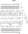
- Figure 2 is a depiction of a second alternative embodiment of a single layer of a multi-layer printed circuit board of the present invention.
- the present invention is of a printed circuit board with embedded decoupling capacitance and a method for producing same.
- printed circuit boards having very high integrated decoupling capacitances are created by the multi-layering within the printed circuit board of pre-drilled or pre-etched conductor foils that have been coated with a dielectric material.
- the pre-drilled or pre-etched conductor foils are in the form of voltage or ground planes. After coating with a dielectric material, they are stacked up in alternate fashion (i.e. voltage/ground/voltage) and laminated together with other signal planes to create the final multi-layer circuit board.
- the conductor foil is of a copper material.
- suitable conductor foils include, but are not limited to, copper-Invar-copper, Invar, aluminum, and copper pre-laminated to a dielectric.
- the dielectric coating may be any type of dielectric material from standard liquid epoxy, polyimide, Teflon, cyanate resins, powdered resin materials, or filled resin systems exhibiting enhanced dielectric constants.
- Coating of the dielectric material onto the conductor foil is performed with any number of methods known in the industry such as roller, draw, powder or curtain coating, electrostatic or electrophoretic deposition, screen printing, spraying, dipping or transfer of a dry film. Any of these coating methods is capable of providing uniformly thin (0.0001" - 0.003") films. Once multi-layer laminated, the thickness of these coated films is not limited by a glass cloth material.
- an Advanced Solder Mask (ASM) dry film material was used to form a composite multi-layer printed circuit board with an integral capacitive stack-up in accordance with the present invention.
- ASM Advanced Solder Mask
- Conventional signal-signal and signal-voltage cores were fabricated through means of lamination and circuitization. These circuitized cores were subjected to a copper oxide process to enhance composite lamination adhesion.
- copper foil/dielectric structures in accordance with the present invention were pre-fabricated as follows:
- Figure 1 shows the printed circuit board constructed as described in Example 1.
- the three copper sheets that were drilled are labeled, 10, 12, and 14, respectively. Copper sheets 10 and 14 were drilled in a ground plane clearance hole pattern. Copper sheet 12 was drilled in a voltage plane clearance hole pattern.
- a sheet of ASM dry film 16 was then laminated to the top surface of copper sheet 10.
- ASM dry film sheets 18 and 20 were laminated on the top and bottom surfaces, respectively, of copper sheet 12.
- ASM dry film sheet 22 was laminated to the bottom surface of copper sheet 14.
- Circuitized core 24 has a signal plane 28 on the top surface and an etched copper foil sheet 30 on the bottom surface.
- the copper foil sheet 30 is etched in a voltage pattern.
- Two layers of epoxy glass 36 and 38, and a copper foil sheet 40 and 42 enclose the top and bottom outer surfaces of the entire printed circuit board.
- each capacitive plane has a dielectric material in between two conductive metal (copper) sheets.
- the resultant structure has two capacitance planes in parallel.
- the resultant structure has a thickness of 0.001", dielectric constant of 40, and a capacitance value of 18 nano-Farads per square inch of board area.
- Figure 2 shows the printed circuit board constructed as described in Example 2.
- the two cores are numbered 52 and 54.
- Core 52 has signal plane 56 on the top surface and etched copper voltage plane 58 on the bottom surface.
- Core 54 has etched copper voltage plane 60 on the top, and signal plane 62 on the bottom. Both etched copper voltage planes 58 and 60 are coated with dielectric material to form layers 64 and 66, respectively.
- the dielectric material as described above, is a filled resin system of BaTiO3 powder, a multifunctional epoxy resin, and MEK solvent. The dielectric material was applied by roller coating. In between the dielectric material layers 64 and 66 is a double treated copper foil sheet 68 drilled in a ground plane clearance hole pattern.
- the outer surfaces of the printed circuit board are formed by two layers of epoxy glass 70, 72 and a copper foil sheet 74 and 76.
- the printed circuit board in Figure 2 has two capacitive planes 78, 80 in parallel with each other.
Applications Claiming Priority (2)
| Application Number | Priority Date | Filing Date | Title |
|---|---|---|---|
| US662164 | 1996-06-12 | ||
| US08/662,164 US5796587A (en) | 1996-06-12 | 1996-06-12 | Printed circut board with embedded decoupling capacitance and method for producing same |
Publications (3)
| Publication Number | Publication Date |
|---|---|
| EP0813355A2 true EP0813355A2 (de) | 1997-12-17 |
| EP0813355A3 EP0813355A3 (de) | 1999-04-14 |
| EP0813355B1 EP0813355B1 (de) | 2002-09-18 |
Family
ID=24656638
Family Applications (1)
| Application Number | Title | Priority Date | Filing Date |
|---|---|---|---|
| EP97304050A Expired - Lifetime EP0813355B1 (de) | 1996-06-12 | 1997-06-11 | Gedruckte Schaltungsplatte mit eingebetteter Entkopplungskapazität und Verfahren zu ihrer Herstellung |
Country Status (8)
| Country | Link |
|---|---|
| US (2) | US5796587A (de) |
| EP (1) | EP0813355B1 (de) |
| JP (1) | JP3400677B2 (de) |
| KR (1) | KR100247717B1 (de) |
| CN (1) | CN1105484C (de) |
| DE (1) | DE69715523T2 (de) |
| MY (1) | MY117854A (de) |
| TW (1) | TW330370B (de) |
Cited By (4)
| Publication number | Priority date | Publication date | Assignee | Title |
|---|---|---|---|---|
| WO2001039562A1 (en) * | 1999-11-23 | 2001-05-31 | Sun Microsystems, Inc. | Printed circuit board employing lossy power distribution network to reduce power plane resonances |
| US6404081B1 (en) | 1998-05-15 | 2002-06-11 | Energenius, Inc. | Embedded backup energy storage unit |
| US6421225B2 (en) | 1998-06-15 | 2002-07-16 | Telefonaktiebolaget Lm Ericsson (Publ) | Electric component |
| US6552265B1 (en) | 1998-10-06 | 2003-04-22 | Telefonaktiebolaget Lm Ericsson | Printed board assembly and method of its manufacture |
Families Citing this family (68)
| Publication number | Priority date | Publication date | Assignee | Title |
|---|---|---|---|---|
| JP2734447B2 (ja) * | 1995-09-14 | 1998-03-30 | 日本電気株式会社 | 多層プリント基板 |
| US6343001B1 (en) | 1996-06-12 | 2002-01-29 | International Business Machines Corporation | Multilayer capacitance structure and circuit board containing the same |
| US20040109298A1 (en) * | 1998-05-04 | 2004-06-10 | Hartman William F. | Dielectric material including particulate filler |
| US6616794B2 (en) * | 1998-05-04 | 2003-09-09 | Tpl, Inc. | Integral capacitance for printed circuit board using dielectric nanopowders |
| US6608760B2 (en) * | 1998-05-04 | 2003-08-19 | Tpl, Inc. | Dielectric material including particulate filler |
| JP3201345B2 (ja) * | 1998-05-13 | 2001-08-20 | 日本電気株式会社 | 多層プリント配線板 |
| US6326677B1 (en) | 1998-09-04 | 2001-12-04 | Cts Corporation | Ball grid array resistor network |
| US6574090B2 (en) | 1998-11-05 | 2003-06-03 | International Business Machines Corporatiion | Printed circuit board capacitor structure and method |
| US6215649B1 (en) * | 1998-11-05 | 2001-04-10 | International Business Machines Corporation | Printed circuit board capacitor structure and method |
| US6005777A (en) * | 1998-11-10 | 1999-12-21 | Cts Corporation | Ball grid array capacitor |
| US6214445B1 (en) * | 1998-12-25 | 2001-04-10 | Ngk Spark Plug Co., Ltd. | Printed wiring board, core substrate, and method for fabricating the core substrate |
| KR100431307B1 (ko) * | 1998-12-29 | 2004-09-18 | 주식회사 하이닉스반도체 | 캐패시터 내장형 칩 사이즈 패키지 및 그의 제조방법 |
| US6274224B1 (en) | 1999-02-01 | 2001-08-14 | 3M Innovative Properties Company | Passive electrical article, circuit articles thereof, and circuit articles comprising a passive electrical article |
| US6542379B1 (en) * | 1999-07-15 | 2003-04-01 | International Business Machines Corporation | Circuitry with integrated passive components and method for producing |
| US6407720B1 (en) * | 1999-07-19 | 2002-06-18 | The United States Of America As Represented By The Secretary Of The Navy | Capacitively loaded quadrifilar helix antenna |
| KR20080111567A (ko) * | 1999-09-02 | 2008-12-23 | 이비덴 가부시키가이샤 | 프린트배선판 및 그 제조방법 |
| CN101232776B (zh) | 1999-09-02 | 2011-04-20 | 揖斐电株式会社 | 印刷布线板 |
| JP3608990B2 (ja) * | 1999-10-19 | 2005-01-12 | 新光電気工業株式会社 | 多層回路基板およびその製造方法 |
| US6367678B1 (en) * | 2000-04-18 | 2002-04-09 | Ballado Investments Inc. | Process for stacking layers that form a multilayer printed circuit |
| US6970362B1 (en) | 2000-07-31 | 2005-11-29 | Intel Corporation | Electronic assemblies and systems comprising interposer with embedded capacitors |
| US6611419B1 (en) | 2000-07-31 | 2003-08-26 | Intel Corporation | Electronic assembly comprising substrate with embedded capacitors |
| US6657849B1 (en) | 2000-08-24 | 2003-12-02 | Oak-Mitsui, Inc. | Formation of an embedded capacitor plane using a thin dielectric |
| US6370012B1 (en) | 2000-08-30 | 2002-04-09 | International Business Machines Corporation | Capacitor laminate for use in printed circuit board and as an interconnector |
| US6775150B1 (en) * | 2000-08-30 | 2004-08-10 | Intel Corporation | Electronic assembly comprising ceramic/organic hybrid substrate with embedded capacitors and methods of manufacture |
| US6548858B2 (en) | 2001-03-06 | 2003-04-15 | Mitac International Corp. | Multi-layer circuit board |
| US6417460B1 (en) * | 2001-03-06 | 2002-07-09 | Mitac International Corp. | Multi-layer circuit board having signal, ground and power layers |
| US6489570B2 (en) * | 2001-03-06 | 2002-12-03 | Mitac International Corp. | Multi-layer circuit board |
| US6384340B1 (en) * | 2001-03-06 | 2002-05-07 | Mitac International Corp. | Multi-layer circuit board |
| SG99360A1 (en) * | 2001-04-19 | 2003-10-27 | Gul Technologies Singapore Ltd | A method for forming a printed circuit board and a printed circuit board formed thereby |
| US6577492B2 (en) | 2001-07-10 | 2003-06-10 | 3M Innovative Properties Company | Capacitor having epoxy dielectric layer cured with aminophenylfluorenes |
| JP3910387B2 (ja) * | 2001-08-24 | 2007-04-25 | 新光電気工業株式会社 | 半導体パッケージ及びその製造方法並びに半導体装置 |
| US20030042044A1 (en) * | 2001-08-30 | 2003-03-06 | Micron Technology, Inc. | Circuit board plane interleave apparatus and method |
| JP4006618B2 (ja) * | 2001-09-26 | 2007-11-14 | 日鉱金属株式会社 | キャリア付銅箔の製法及びキャリア付銅箔を使用したプリント基板 |
| US20030070931A1 (en) * | 2001-10-17 | 2003-04-17 | Honeywell Advanced Circuits, Inc. | Selective plating of printed circuit boards |
| DE10153094A1 (de) * | 2001-10-30 | 2003-05-15 | Bodenseewerk Geraetetech | Optischer Sensor mit einem Sensorstrahlengang und einem parallel zu der optischen Achse des Sensorstrahlenganges emittierenden Laserstrahler |
| JP2003332749A (ja) * | 2002-01-11 | 2003-11-21 | Denso Corp | 受動素子内蔵基板、その製造方法及び受動素子内蔵基板形成用素板 |
| US6941649B2 (en) * | 2002-02-05 | 2005-09-13 | Force10 Networks, Inc. | Method of fabricating a high-layer-count backplane |
| JP4243117B2 (ja) * | 2002-08-27 | 2009-03-25 | 新光電気工業株式会社 | 半導体パッケージとその製造方法および半導体装置 |
| US6844505B1 (en) | 2002-11-04 | 2005-01-18 | Ncr Corporation | Reducing noise effects in circuit boards |
| TWI262204B (en) * | 2003-05-14 | 2006-09-21 | Eternal Chemical Co Ltd | Resin composition having high dielectric constant and uses thereof |
| US7626828B1 (en) | 2003-07-30 | 2009-12-01 | Teradata Us, Inc. | Providing a resistive element between reference plane layers in a circuit board |
| US7180186B2 (en) * | 2003-07-31 | 2007-02-20 | Cts Corporation | Ball grid array package |
| US6946733B2 (en) * | 2003-08-13 | 2005-09-20 | Cts Corporation | Ball grid array package having testing capability after mounting |
| US7056800B2 (en) * | 2003-12-15 | 2006-06-06 | Motorola, Inc. | Printed circuit embedded capacitors |
| US20060074164A1 (en) * | 2003-12-19 | 2006-04-06 | Tpl, Inc. | Structured composite dielectrics |
| US20060074166A1 (en) * | 2003-12-19 | 2006-04-06 | Tpl, Inc. Title And Interest In An Application | Moldable high dielectric constant nano-composites |
| US20080128961A1 (en) * | 2003-12-19 | 2008-06-05 | Tpl, Inc. | Moldable high dielectric constant nano-composites |
| TWI314745B (en) | 2004-02-02 | 2009-09-11 | Ind Tech Res Inst | Method and apparatus of non-symmetrical electrode of build-in capacitor |
| US7776194B2 (en) * | 2004-04-16 | 2010-08-17 | Denso Corporation | Gas concentration measuring apparatus designed to compensate for output error |
| US9572258B2 (en) * | 2004-12-30 | 2017-02-14 | Intel Corporation | Method of forming a substrate core with embedded capacitor and structures formed thereby |
| US20070177331A1 (en) * | 2005-01-10 | 2007-08-02 | Endicott Interconnect Technologies, Inc. | Non-flaking capacitor material, capacitive substrate having an internal capacitor therein including said non-flaking capacitor material, and method of making a capacitor member for use in a capacitive substrate |
| US8607445B1 (en) | 2005-01-10 | 2013-12-17 | Endicott Interconnect Technologies, Inc. | Substrate having internal capacitor and method of making same |
| US7138068B2 (en) * | 2005-03-21 | 2006-11-21 | Motorola, Inc. | Printed circuit patterned embedded capacitance layer |
| KR100843392B1 (ko) * | 2005-03-31 | 2008-07-03 | 삼성전기주식회사 | 우수한 내구성을 갖는 인쇄회로기판용 임프린트 몰드 및이를 이용한 인쇄회로기판의 제조방법 |
| KR100716824B1 (ko) * | 2005-04-28 | 2007-05-09 | 삼성전기주식회사 | 하이브리드 재료를 이용한 커패시터 내장형 인쇄회로기판및 그 제조방법 |
| WO2007043972A1 (en) * | 2005-10-12 | 2007-04-19 | Agency For Science, Technology And Research | Device carrying an integrated circuit/components and method of producing the same |
| US7336501B2 (en) * | 2006-06-26 | 2008-02-26 | Ibiden Co., Ltd. | Wiring board with built-in capacitor |
| CN101207104B (zh) * | 2006-12-19 | 2011-08-24 | 成都锐华光电技术有限责任公司 | 埋入式电容超低电感设计 |
| US7791896B1 (en) | 2007-06-20 | 2010-09-07 | Teradata Us, Inc. | Providing an embedded capacitor in a circuit board |
| US7886414B2 (en) * | 2007-07-23 | 2011-02-15 | Samsung Electro-Mechanics Co., Ltd. | Method of manufacturing capacitor-embedded PCB |
| US8325461B2 (en) * | 2008-08-08 | 2012-12-04 | Hamilton Sundstrand Corporation | Printed wiring board feed-through capacitor |
| US10176162B2 (en) * | 2009-02-27 | 2019-01-08 | Blackberry Limited | System and method for improved address entry |
| US8409963B2 (en) * | 2009-04-28 | 2013-04-02 | CDA Procesing Limited Liability Company | Methods of embedding thin-film capacitors into semiconductor packages using temporary carrier layers |
| US8391017B2 (en) * | 2009-04-28 | 2013-03-05 | Georgia Tech Research Corporation | Thin-film capacitor structures embedded in semiconductor packages and methods of making |
| CN106376170A (zh) * | 2015-07-24 | 2017-02-01 | 宏启胜精密电子(秦皇岛)有限公司 | 柔性电路板及其制作方法、电子装置 |
| US10083781B2 (en) | 2015-10-30 | 2018-09-25 | Vishay Dale Electronics, Llc | Surface mount resistors and methods of manufacturing same |
| US10575395B2 (en) | 2016-06-07 | 2020-02-25 | Honeywell International Inc. | Band pass filter-based galvanic isolator |
| US10438729B2 (en) | 2017-11-10 | 2019-10-08 | Vishay Dale Electronics, Llc | Resistor with upper surface heat dissipation |
Citations (4)
| Publication number | Priority date | Publication date | Assignee | Title |
|---|---|---|---|---|
| US4574255A (en) * | 1982-12-15 | 1986-03-04 | Nec Corporation | MMC Substrate including capacitors having perovskite structure dielectric and electrical devices including MMC substrate |
| US5079069A (en) * | 1989-08-23 | 1992-01-07 | Zycon Corporation | Capacitor laminate for use in capacitive printed circuit boards and methods of manufacture |
| US5161086A (en) * | 1989-08-23 | 1992-11-03 | Zycon Corporation | Capacitor laminate for use in capacitive printed circuit boards and methods of manufacture |
| US5261153A (en) * | 1992-04-06 | 1993-11-16 | Zycon Corporation | In situ method for forming a capacitive PCB |
Family Cites Families (22)
| Publication number | Priority date | Publication date | Assignee | Title |
|---|---|---|---|---|
| US3635759A (en) * | 1969-04-04 | 1972-01-18 | Gulton Ind Inc | Method of eliminating voids in ceramic bodies |
| US4035768A (en) * | 1976-05-03 | 1977-07-12 | Veripen, Inc. | Personal identification apparatus |
| US4241378A (en) * | 1978-06-12 | 1980-12-23 | Erie Technological Products, Inc. | Base metal electrode capacitor and method of making the same |
| US4792779A (en) * | 1986-09-19 | 1988-12-20 | Hughes Aircraft Company | Trimming passive components buried in multilayer structures |
| US4775573A (en) * | 1987-04-03 | 1988-10-04 | West-Tronics, Inc. | Multilayer PC board using polymer thick films |
| US4835656A (en) * | 1987-04-04 | 1989-05-30 | Mitsubishi Mining And Cement Co., Ltd. | Multi-layered ceramic capacitor |
| JPH0648666B2 (ja) * | 1987-09-29 | 1994-06-22 | 三菱マテリアル株式会社 | 積層セラミックコンデンサ及びその製法 |
| US4864465A (en) * | 1988-05-10 | 1989-09-05 | The United States Of America | Viad chip capacitor and method for making same |
| US5010641A (en) * | 1989-06-30 | 1991-04-30 | Unisys Corp. | Method of making multilayer printed circuit board |
| US5155655A (en) * | 1989-08-23 | 1992-10-13 | Zycon Corporation | Capacitor laminate for use in capacitive printed circuit boards and methods of manufacture |
| JP2868576B2 (ja) * | 1990-03-30 | 1999-03-10 | 株式会社東芝 | 多層配線基板 |
| US5027253A (en) * | 1990-04-09 | 1991-06-25 | Ibm Corporation | Printed circuit boards and cards having buried thin film capacitors and processing techniques for fabricating said boards and cards |
| JP3019541B2 (ja) * | 1990-11-22 | 2000-03-13 | 株式会社村田製作所 | コンデンサ内蔵型配線基板およびその製造方法 |
| US5072329A (en) * | 1991-04-01 | 1991-12-10 | Avx Corporation | Delamination resistant ceramic capacitor and method of making same |
| US5144526A (en) * | 1991-08-05 | 1992-09-01 | Hughes Aircraft Company | Low temperature co-fired ceramic structure containing buried capacitors |
| US5162977A (en) * | 1991-08-27 | 1992-11-10 | Storage Technology Corporation | Printed circuit board having an integrated decoupling capacitive element |
| US5206788A (en) * | 1991-12-12 | 1993-04-27 | Ramtron Corporation | Series ferroelectric capacitor structure for monolithic integrated circuits and method |
| US5282312A (en) * | 1991-12-31 | 1994-02-01 | Tessera, Inc. | Multi-layer circuit construction methods with customization features |
| US5800575A (en) * | 1992-04-06 | 1998-09-01 | Zycon Corporation | In situ method of forming a bypass capacitor element internally within a capacitive PCB |
| WO1994002310A1 (en) * | 1992-07-16 | 1994-02-03 | Zycon Corporation | Printed circuit board with internal capacitor |
| US5428499A (en) * | 1993-01-28 | 1995-06-27 | Storage Technology Corporation | Printed circuit board having integrated decoupling capacitive core with discrete elements |
| US5469324A (en) * | 1994-10-07 | 1995-11-21 | Storage Technology Corporation | Integrated decoupling capacitive core for a printed circuit board and method of making same |
-
1996
- 1996-06-12 US US08/662,164 patent/US5796587A/en not_active Expired - Lifetime
- 1996-11-09 TW TW085113696A patent/TW330370B/zh active
-
1997
- 1997-04-18 KR KR1019970014421A patent/KR100247717B1/ko not_active IP Right Cessation
- 1997-05-20 MY MYPI97002207A patent/MY117854A/en unknown
- 1997-05-22 CN CN97113438A patent/CN1105484C/zh not_active Expired - Lifetime
- 1997-06-05 JP JP14758197A patent/JP3400677B2/ja not_active Expired - Lifetime
- 1997-06-11 EP EP97304050A patent/EP0813355B1/de not_active Expired - Lifetime
- 1997-06-11 DE DE69715523T patent/DE69715523T2/de not_active Expired - Fee Related
-
1998
- 1998-02-11 US US09/022,258 patent/US6256850B1/en not_active Expired - Fee Related
Patent Citations (4)
| Publication number | Priority date | Publication date | Assignee | Title |
|---|---|---|---|---|
| US4574255A (en) * | 1982-12-15 | 1986-03-04 | Nec Corporation | MMC Substrate including capacitors having perovskite structure dielectric and electrical devices including MMC substrate |
| US5079069A (en) * | 1989-08-23 | 1992-01-07 | Zycon Corporation | Capacitor laminate for use in capacitive printed circuit boards and methods of manufacture |
| US5161086A (en) * | 1989-08-23 | 1992-11-03 | Zycon Corporation | Capacitor laminate for use in capacitive printed circuit boards and methods of manufacture |
| US5261153A (en) * | 1992-04-06 | 1993-11-16 | Zycon Corporation | In situ method for forming a capacitive PCB |
Cited By (7)
| Publication number | Priority date | Publication date | Assignee | Title |
|---|---|---|---|---|
| US6404081B1 (en) | 1998-05-15 | 2002-06-11 | Energenius, Inc. | Embedded backup energy storage unit |
| EP1078437B1 (de) * | 1998-05-15 | 2003-05-02 | Energenius, Inc. | Eingebettene reserveenergiespeichereinheit |
| US6421225B2 (en) | 1998-06-15 | 2002-07-16 | Telefonaktiebolaget Lm Ericsson (Publ) | Electric component |
| US6552265B1 (en) | 1998-10-06 | 2003-04-22 | Telefonaktiebolaget Lm Ericsson | Printed board assembly and method of its manufacture |
| WO2001039562A1 (en) * | 1999-11-23 | 2001-05-31 | Sun Microsystems, Inc. | Printed circuit board employing lossy power distribution network to reduce power plane resonances |
| US6441313B1 (en) | 1999-11-23 | 2002-08-27 | Sun Microsystems, Inc. | Printed circuit board employing lossy power distribution network to reduce power plane resonances |
| US6753481B2 (en) | 1999-11-23 | 2004-06-22 | Sun Microsystems, Inc. | Printed circuit board employing lossy power distribution network to reduce power plane resonances |
Also Published As
| Publication number | Publication date |
|---|---|
| MY117854A (en) | 2004-08-30 |
| US6256850B1 (en) | 2001-07-10 |
| KR100247717B1 (ko) | 2000-03-15 |
| CN1105484C (zh) | 2003-04-09 |
| TW330370B (en) | 1998-04-21 |
| EP0813355B1 (de) | 2002-09-18 |
| DE69715523D1 (de) | 2002-10-24 |
| CN1173803A (zh) | 1998-02-18 |
| JP3400677B2 (ja) | 2003-04-28 |
| EP0813355A3 (de) | 1999-04-14 |
| KR980006256A (ko) | 1998-03-30 |
| JPH1056249A (ja) | 1998-02-24 |
| US5796587A (en) | 1998-08-18 |
| DE69715523T2 (de) | 2003-05-28 |
Similar Documents
| Publication | Publication Date | Title |
|---|---|---|
| EP0813355B1 (de) | Gedruckte Schaltungsplatte mit eingebetteter Entkopplungskapazität und Verfahren zu ihrer Herstellung | |
| KR100562812B1 (ko) | 커패시터를 갖는 인쇄 배선 기판 및 그 제조 방법 | |
| KR100716824B1 (ko) | 하이브리드 재료를 이용한 커패시터 내장형 인쇄회로기판및 그 제조방법 | |
| US5261153A (en) | In situ method for forming a capacitive PCB | |
| US8713769B2 (en) | Embedded capacitive stack | |
| JP2006060187A (ja) | キャパシタ内蔵型プリント回路基板及びその製造方法 | |
| KR20080031298A (ko) | 수동 전기 물품 | |
| KR100861618B1 (ko) | 내장형 캐패시터의 공차 향상을 위한 인쇄회로기판 및 그제조방법 | |
| US20020080556A1 (en) | Multilayer capacitance structure and circuit board containing the same and method of forming the same | |
| US6739027B1 (en) | Method for producing printed circuit board with embedded decoupling capacitance | |
| US6574090B2 (en) | Printed circuit board capacitor structure and method | |
| US5709805A (en) | Method for producing multi-layer circuit board and resulting article of manufacture | |
| JP3199664B2 (ja) | 多層配線基板の製造方法 | |
| US20040108134A1 (en) | Printed wiring boards having low inductance embedded capacitors and methods of making same | |
| KR100713731B1 (ko) | 낮은 인덕턴스의 내장 커패시터를 구비한 인쇄 배선 기판및 그 제조 방법 | |
| KR100645613B1 (ko) | 캐패시터 내장형 인쇄회로기판 및 그 제조 방법 | |
| US8501575B2 (en) | Method of forming multilayer capacitors in a printed circuit substrate | |
| JP2004172530A (ja) | 誘電体積層シート、基板内蔵キャパシターシート及び素子内蔵基板 | |
| WO1994002310A1 (en) | Printed circuit board with internal capacitor | |
| WO2003100852A1 (fr) | Fil metallique de blindage dans une carte multicouches, puce a semi-conducteurs, element de circuit electronique et procede de production de ce fil | |
| JP2005129887A (ja) | コンデンサを有する印刷配線板とその製造方法 |
Legal Events
| Date | Code | Title | Description |
|---|---|---|---|
| PUAI | Public reference made under article 153(3) epc to a published international application that has entered the european phase |
Free format text: ORIGINAL CODE: 0009012 |
|
| AK | Designated contracting states |
Kind code of ref document: A2 Designated state(s): DE FR GB |
|
| PUAL | Search report despatched |
Free format text: ORIGINAL CODE: 0009013 |
|
| AK | Designated contracting states |
Kind code of ref document: A3 Designated state(s): AT BE CH DE DK ES FI FR GB GR IE IT LI LU MC NL PT SE |
|
| 17P | Request for examination filed |
Effective date: 19991012 |
|
| AKX | Designation fees paid |
Free format text: DE FR GB |
|
| 17Q | First examination report despatched |
Effective date: 20000926 |
|
| GRAG | Despatch of communication of intention to grant |
Free format text: ORIGINAL CODE: EPIDOS AGRA |
|
| GRAG | Despatch of communication of intention to grant |
Free format text: ORIGINAL CODE: EPIDOS AGRA |
|
| GRAH | Despatch of communication of intention to grant a patent |
Free format text: ORIGINAL CODE: EPIDOS IGRA |
|
| GRAH | Despatch of communication of intention to grant a patent |
Free format text: ORIGINAL CODE: EPIDOS IGRA |
|
| GRAA | (expected) grant |
Free format text: ORIGINAL CODE: 0009210 |
|
| AK | Designated contracting states |
Kind code of ref document: B1 Designated state(s): DE FR GB |
|
| REG | Reference to a national code |
Ref country code: GB Ref legal event code: FG4D |
|
| REF | Corresponds to: |
Ref document number: 69715523 Country of ref document: DE Date of ref document: 20021024 |
|
| ET | Fr: translation filed | ||
| PGFP | Annual fee paid to national office [announced via postgrant information from national office to epo] |
Ref country code: GB Payment date: 20030602 Year of fee payment: 7 |
|
| PGFP | Annual fee paid to national office [announced via postgrant information from national office to epo] |
Ref country code: DE Payment date: 20030624 Year of fee payment: 7 |
|
| PLBE | No opposition filed within time limit |
Free format text: ORIGINAL CODE: 0009261 |
|
| STAA | Information on the status of an ep patent application or granted ep patent |
Free format text: STATUS: NO OPPOSITION FILED WITHIN TIME LIMIT |
|
| 26N | No opposition filed |
Effective date: 20030619 |
|
| PG25 | Lapsed in a contracting state [announced via postgrant information from national office to epo] |
Ref country code: FR Free format text: LAPSE BECAUSE OF NON-PAYMENT OF DUE FEES Effective date: 20040227 |
|
| REG | Reference to a national code |
Ref country code: FR Ref legal event code: ST |
|
| PG25 | Lapsed in a contracting state [announced via postgrant information from national office to epo] |
Ref country code: GB Free format text: LAPSE BECAUSE OF NON-PAYMENT OF DUE FEES Effective date: 20040611 |
|
| PG25 | Lapsed in a contracting state [announced via postgrant information from national office to epo] |
Ref country code: DE Free format text: LAPSE BECAUSE OF NON-PAYMENT OF DUE FEES Effective date: 20050101 |
|
| GBPC | Gb: european patent ceased through non-payment of renewal fee |
Effective date: 20040611 |
|
| REG | Reference to a national code |
Ref country code: DE Ref legal event code: R081 Ref document number: 69715523 Country of ref document: DE Owner name: GLOBALFOUNDRIES INC., KY Free format text: FORMER OWNER: INTERNATIONAL BUSINESS MACHINES CORPORATION, ARMONK, NY, US Ref country code: DE Ref legal event code: R082 Ref document number: 69715523 Country of ref document: DE Representative=s name: RICHARDT PATENTANWAELTE PARTG MBB, DE Ref country code: DE Ref legal event code: R081 Ref document number: 69715523 Country of ref document: DE Owner name: GLOBALFOUNDRIES INC., KY Free format text: FORMER OWNER: INTERNATIONAL BUSINESS MACHINES CORPORATION, ARMONK, N.Y., US |
|
| REG | Reference to a national code |
Ref country code: DE Ref legal event code: R082 Ref document number: 69715523 Country of ref document: DE Representative=s name: RICHARDT PATENTANWAELTE PARTG MBB, DE Ref country code: DE Ref legal event code: R081 Ref document number: 69715523 Country of ref document: DE Owner name: GLOBALFOUNDRIES INC., KY Free format text: FORMER OWNER: GLOBALFOUNDRIES US 2 LLC (N.D.GES.DES STAATES DELAWARE), HOPEWELL JUNCTION, N.Y., US |
|
| REG | Reference to a national code |
Ref country code: FR Ref legal event code: TP Owner name: GLOBALFOUNDRIES INC., GB Effective date: 20160829 |