EP0813232B1 - Procédé de réduction de la quantité de carbone à l'interface entre un film epitaxial et un substrat Si - Google Patents
Procédé de réduction de la quantité de carbone à l'interface entre un film epitaxial et un substrat Si Download PDFInfo
- Publication number
- EP0813232B1 EP0813232B1 EP97107876A EP97107876A EP0813232B1 EP 0813232 B1 EP0813232 B1 EP 0813232B1 EP 97107876 A EP97107876 A EP 97107876A EP 97107876 A EP97107876 A EP 97107876A EP 0813232 B1 EP0813232 B1 EP 0813232B1
- Authority
- EP
- European Patent Office
- Prior art keywords
- substrate
- carbon
- manufacturing
- epitaxial film
- semiconductor device
- Prior art date
- Legal status (The legal status is an assumption and is not a legal conclusion. Google has not performed a legal analysis and makes no representation as to the accuracy of the status listed.)
- Expired - Lifetime
Links
Images


Classifications
-
- C—CHEMISTRY; METALLURGY
- C30—CRYSTAL GROWTH
- C30B—SINGLE-CRYSTAL GROWTH; UNIDIRECTIONAL SOLIDIFICATION OF EUTECTIC MATERIAL OR UNIDIRECTIONAL DEMIXING OF EUTECTOID MATERIAL; REFINING BY ZONE-MELTING OF MATERIAL; PRODUCTION OF A HOMOGENEOUS POLYCRYSTALLINE MATERIAL WITH DEFINED STRUCTURE; SINGLE CRYSTALS OR HOMOGENEOUS POLYCRYSTALLINE MATERIAL WITH DEFINED STRUCTURE; AFTER-TREATMENT OF SINGLE CRYSTALS OR A HOMOGENEOUS POLYCRYSTALLINE MATERIAL WITH DEFINED STRUCTURE; APPARATUS THEREFOR
- C30B29/00—Single crystals or homogeneous polycrystalline material with defined structure characterised by the material or by their shape
- C30B29/02—Elements
- C30B29/06—Silicon
-
- C—CHEMISTRY; METALLURGY
- C30—CRYSTAL GROWTH
- C30B—SINGLE-CRYSTAL GROWTH; UNIDIRECTIONAL SOLIDIFICATION OF EUTECTIC MATERIAL OR UNIDIRECTIONAL DEMIXING OF EUTECTOID MATERIAL; REFINING BY ZONE-MELTING OF MATERIAL; PRODUCTION OF A HOMOGENEOUS POLYCRYSTALLINE MATERIAL WITH DEFINED STRUCTURE; SINGLE CRYSTALS OR HOMOGENEOUS POLYCRYSTALLINE MATERIAL WITH DEFINED STRUCTURE; AFTER-TREATMENT OF SINGLE CRYSTALS OR A HOMOGENEOUS POLYCRYSTALLINE MATERIAL WITH DEFINED STRUCTURE; APPARATUS THEREFOR
- C30B25/00—Single-crystal growth by chemical reaction of reactive gases, e.g. chemical vapour-deposition growth
- C30B25/02—Epitaxial-layer growth
- C30B25/18—Epitaxial-layer growth characterised by the substrate
-
- H—ELECTRICITY
- H10—SEMICONDUCTOR DEVICES; ELECTRIC SOLID-STATE DEVICES NOT OTHERWISE PROVIDED FOR
- H10P—GENERIC PROCESSES OR APPARATUS FOR THE MANUFACTURE OR TREATMENT OF DEVICES COVERED BY CLASS H10
- H10P14/00—Formation of materials, e.g. in the shape of layers or pillars
- H10P14/20—Formation of materials, e.g. in the shape of layers or pillars of semiconductor materials
- H10P14/24—Formation of materials, e.g. in the shape of layers or pillars of semiconductor materials using chemical vapour deposition [CVD]
-
- H—ELECTRICITY
- H10—SEMICONDUCTOR DEVICES; ELECTRIC SOLID-STATE DEVICES NOT OTHERWISE PROVIDED FOR
- H10P—GENERIC PROCESSES OR APPARATUS FOR THE MANUFACTURE OR TREATMENT OF DEVICES COVERED BY CLASS H10
- H10P14/00—Formation of materials, e.g. in the shape of layers or pillars
- H10P14/20—Formation of materials, e.g. in the shape of layers or pillars of semiconductor materials
- H10P14/29—Formation of materials, e.g. in the shape of layers or pillars of semiconductor materials characterised by the substrates
- H10P14/2901—Materials
- H10P14/2902—Materials being Group IVA materials
- H10P14/2905—Silicon, silicon germanium or germanium
-
- H—ELECTRICITY
- H10—SEMICONDUCTOR DEVICES; ELECTRIC SOLID-STATE DEVICES NOT OTHERWISE PROVIDED FOR
- H10P—GENERIC PROCESSES OR APPARATUS FOR THE MANUFACTURE OR TREATMENT OF DEVICES COVERED BY CLASS H10
- H10P14/00—Formation of materials, e.g. in the shape of layers or pillars
- H10P14/20—Formation of materials, e.g. in the shape of layers or pillars of semiconductor materials
- H10P14/34—Deposited materials, e.g. layers
- H10P14/3402—Deposited materials, e.g. layers characterised by the chemical composition
- H10P14/3404—Deposited materials, e.g. layers characterised by the chemical composition being Group IVA materials
- H10P14/3411—Silicon, silicon germanium or germanium
Definitions
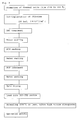
- Fig. 5 is a sectional view of a high-speed bipolar transistor of a Si 1-x Ge x epitaxial film base which is used in the evaluation of a cut-off frequency.
Landscapes
- Chemical & Material Sciences (AREA)
- Engineering & Computer Science (AREA)
- Crystallography & Structural Chemistry (AREA)
- Materials Engineering (AREA)
- Metallurgy (AREA)
- Organic Chemistry (AREA)
- Chemical Kinetics & Catalysis (AREA)
- General Chemical & Material Sciences (AREA)
- Crystals, And After-Treatments Of Crystals (AREA)
Claims (6)
- Procédé de fabrication d'un dispositif à semiconducteur comprenant les étapes séquentielles, dans lesquelles :a) on pratique une implantation ionique, dans un substrat en Si, d'un élément ou d'un composé qui réagit avec du carbone lors d'une étape de recuit ultérieure,b) on lave le substrat en Si de l'étape a) pour éliminer des particules et des substances organiques restant sur le substrat en Si après l'étape d'implantation ionique, ledit lavage ayant pour conséquence la formation d'un film d'oxyde naturel sur le substrat en Si,c) on élimine le film d'oxyde naturel se trouvant sur le substrat en Si,d) on recuit le substrat en Si, que l'on a soumis à l'implantation ionique à l'étape a), au lavage à l'étape b) et à l'élimination du film d'oxyde naturel à l'étape c), à une température de 800 °C, ou moins, dans un dispositif de CVD ; ete) on effectue une croissance épitaxiale de Si, ou une croissance épitaxiale de Si1-xGex, sur le substrat recuit à l'étape d) dans le dispositif de CVD.
- Procédé de fabrication d'un dispositif à semiconducteur selon la revendication 1, dans lequel l'étape b) de lavage utilise une solution d'eau pure de peroxyde d'hydrogène ammoniacal.
- Procédé de fabrication d'un dispositif à semiconducteur selon la revendication 1 ou 2, dans lequel l'élément ou le composé qui réagit avec du carbone à l'étape d) est un élément ou un composé choisi dans le groupe constitué de l'oxygène, de l'hydrogène, d'halogènes et de leurs composés.
- Procédé de fabrication d'un dispositif à semiconducteur selon la revendication 3, dans lequel l'halogène est du chlore.
- Procédé de fabrication d'un dispositif à semiconducteur selon la revendication 1, dans lequel la croissance épitaxiale effectuée dans le dispositif de CVD se fait par utilisation, en tant que matériau, d'un ou de plusieurs des composés choisis dans le groupe constitué d'hybrides de Si, de Ge et de B.
- Procédé de fabrication d'un dispositif à semiconducteur selon la revendication 5, dans lequel la croissance épitaxiale est effectuée par utilisation de SiH4, de Si2H6, de GeH4 et/ou de B2H6.
Applications Claiming Priority (3)
| Application Number | Priority Date | Filing Date | Title |
|---|---|---|---|
| JP8120131A JP2836576B2 (ja) | 1996-05-15 | 1996-05-15 | 半導体装置の製造方法 |
| JP120131/96 | 1996-05-15 | ||
| JP12013196 | 1996-05-15 |
Publications (3)
| Publication Number | Publication Date |
|---|---|
| EP0813232A2 EP0813232A2 (fr) | 1997-12-17 |
| EP0813232A3 EP0813232A3 (fr) | 1998-09-02 |
| EP0813232B1 true EP0813232B1 (fr) | 2002-09-25 |
Family
ID=14778747
Family Applications (1)
| Application Number | Title | Priority Date | Filing Date |
|---|---|---|---|
| EP97107876A Expired - Lifetime EP0813232B1 (fr) | 1996-05-15 | 1997-05-14 | Procédé de réduction de la quantité de carbone à l'interface entre un film epitaxial et un substrat Si |
Country Status (4)
| Country | Link |
|---|---|
| US (1) | US5920795A (fr) |
| EP (1) | EP0813232B1 (fr) |
| JP (1) | JP2836576B2 (fr) |
| DE (1) | DE69715735T2 (fr) |
Families Citing this family (7)
| Publication number | Priority date | Publication date | Assignee | Title |
|---|---|---|---|---|
| FR2774509B1 (fr) * | 1998-01-30 | 2001-11-16 | Sgs Thomson Microelectronics | Procede de depot d'une region de silicium monocristallin |
| US6143073A (en) * | 1998-11-19 | 2000-11-07 | Heraeus Shin-Etsu America | Methods and apparatus for minimizing white point defects in quartz glass crucibles |
| EP1235258A4 (fr) * | 1999-10-29 | 2007-03-28 | Matsushita Electric Industrial Co Ltd | Procede de nettoyage de substrat et procede de fabrication de dispositif semi-conducteur |
| US6406929B1 (en) * | 2000-06-21 | 2002-06-18 | University Of Vermont And State Agricultural College | Structure and method for abrupt PN junction diode formed using chemical vapor deposition processing |
| JP2003086554A (ja) * | 2001-09-11 | 2003-03-20 | Mitsubishi Heavy Ind Ltd | 半導体基板の製造装置、及び、その製造方法 |
| KR100678468B1 (ko) * | 2005-01-14 | 2007-02-02 | 삼성전자주식회사 | 반도체 기판의 인-시츄 세정방법 및 이를 채택하는 반도체소자의 제조방법 |
| KR100632460B1 (ko) * | 2005-02-03 | 2006-10-11 | 삼성전자주식회사 | 반도체 소자의 제조 방법 |
Family Cites Families (9)
| Publication number | Priority date | Publication date | Assignee | Title |
|---|---|---|---|---|
| JPH0644562B2 (ja) * | 1985-05-24 | 1994-06-08 | 日本電気株式会社 | 表面清浄化方法 |
| JP2595935B2 (ja) * | 1985-12-13 | 1997-04-02 | 日本電気株式会社 | 表面清浄化方法 |
| US4717681A (en) * | 1986-05-19 | 1988-01-05 | Texas Instruments Incorporated | Method of making a heterojunction bipolar transistor with SIPOS |
| JPS6348817A (ja) * | 1986-08-19 | 1988-03-01 | Fujitsu Ltd | エピタキシヤル成長方法 |
| JPS6351641A (ja) * | 1986-08-21 | 1988-03-04 | Oki Electric Ind Co Ltd | 単結晶または多結晶Si膜の微細パタ−ン形成方法 |
| JPS6410616A (en) * | 1987-07-02 | 1989-01-13 | Nec Corp | Method and device for growth of compound semiconductor crystal |
| JPS6423538A (en) * | 1987-07-20 | 1989-01-26 | Nec Corp | Method and equipment for manufacturing semiconductor device |
| JPH04304635A (ja) * | 1991-04-01 | 1992-10-28 | Hitachi Ltd | 基板清浄化装置を有する半導体製造方法およびその装置 |
| US5516710A (en) * | 1994-11-10 | 1996-05-14 | Northern Telecom Limited | Method of forming a transistor |
-
1996
- 1996-05-15 JP JP8120131A patent/JP2836576B2/ja not_active Expired - Fee Related
-
1997
- 1997-05-05 US US08/851,366 patent/US5920795A/en not_active Expired - Lifetime
- 1997-05-14 EP EP97107876A patent/EP0813232B1/fr not_active Expired - Lifetime
- 1997-05-14 DE DE69715735T patent/DE69715735T2/de not_active Expired - Fee Related
Also Published As
| Publication number | Publication date |
|---|---|
| EP0813232A2 (fr) | 1997-12-17 |
| EP0813232A3 (fr) | 1998-09-02 |
| DE69715735D1 (de) | 2002-10-31 |
| DE69715735T2 (de) | 2003-05-22 |
| JP2836576B2 (ja) | 1998-12-14 |
| US5920795A (en) | 1999-07-06 |
| JPH09306847A (ja) | 1997-11-28 |
Similar Documents
| Publication | Publication Date | Title |
|---|---|---|
| EP0090940B1 (fr) | Procédé de réalisation de régions émetteur et base intrinsique d'un transistor bipolaire | |
| US5821158A (en) | Substrate surface treatment method capable of removing a spontaneous oxide film at a relatively low temperature | |
| US5731626A (en) | Process for controlling dopant diffusion in a semiconductor layer and semiconductor layer formed thereby | |
| US6368927B1 (en) | Method of manufacturing transistor having elevated source and drain regions | |
| KR100678468B1 (ko) | 반도체 기판의 인-시츄 세정방법 및 이를 채택하는 반도체소자의 제조방법 | |
| JP3079575B2 (ja) | 半導体装置の製造方法 | |
| US6358865B2 (en) | Oxidation of silicon using fluorine implant | |
| US5565690A (en) | Method for doping strained heterojunction semiconductor devices and structure | |
| EP0813232B1 (fr) | Procédé de réduction de la quantité de carbone à l'interface entre un film epitaxial et un substrat Si | |
| JPH0684819A (ja) | 高濃度にドープされた半導体物質の製造方法 | |
| US6228166B1 (en) | Method for boron contamination reduction in IC fabrication | |
| US7556048B2 (en) | In-situ removal of surface impurities prior to arsenic-doped polysilicon deposition in the fabrication of a heterojunction bipolar transistor | |
| US5674777A (en) | Method for forming silicon-boron binary compound layer as boron diffusion source in silicon electronic device | |
| US6703283B1 (en) | Discontinuous dielectric interface for bipolar transistors | |
| JP2920546B2 (ja) | 同極ゲートmisトランジスタの製造方法 | |
| KR100333727B1 (ko) | 엘리베이티드소오스/드레인구조의모스트랜지스터제조방법 | |
| JP2973949B2 (ja) | 半導体装置の製造方法 | |
| EP1052685A2 (fr) | Composant de circuit intégré comprenant une couche d'oxide implantée avec du fluor | |
| JPH05251378A (ja) | 半導体装置の製造方法 | |
| Donahue et al. | Low Temperature Silicon Epitaxy Deposited by Very Low Pressure Chemical Vapor Deposition: II. Autodoping | |
| Kiyota et al. | Reduction of base resistance and increase in cutoff frequency of Si bipolar transistor using rapid vapor-phase doping | |
| JP2956616B2 (ja) | 半導体装置の製造方法 | |
| Topich | Reduction of Defects in Ion Implanted Bipolar Transistors by Argon Back Side Damage | |
| Theunissen et al. | Boron Vapour Phase Doping of Silicon for Bipolar Device Applications | |
| KR100269716B1 (ko) | Ic 제조시 붕소 오염량 감소방법 |
Legal Events
| Date | Code | Title | Description |
|---|---|---|---|
| PUAI | Public reference made under article 153(3) epc to a published international application that has entered the european phase |
Free format text: ORIGINAL CODE: 0009012 |
|
| AK | Designated contracting states |
Kind code of ref document: A2 Designated state(s): DE FR GB |
|
| PUAL | Search report despatched |
Free format text: ORIGINAL CODE: 0009013 |
|
| AK | Designated contracting states |
Kind code of ref document: A3 Designated state(s): DE FR GB |
|
| 17P | Request for examination filed |
Effective date: 19980729 |
|
| 17Q | First examination report despatched |
Effective date: 19991201 |
|
| GRAG | Despatch of communication of intention to grant |
Free format text: ORIGINAL CODE: EPIDOS AGRA |
|
| GRAG | Despatch of communication of intention to grant |
Free format text: ORIGINAL CODE: EPIDOS AGRA |
|
| GRAH | Despatch of communication of intention to grant a patent |
Free format text: ORIGINAL CODE: EPIDOS IGRA |
|
| GRAH | Despatch of communication of intention to grant a patent |
Free format text: ORIGINAL CODE: EPIDOS IGRA |
|
| GRAA | (expected) grant |
Free format text: ORIGINAL CODE: 0009210 |
|
| AK | Designated contracting states |
Kind code of ref document: B1 Designated state(s): DE FR GB |
|
| REG | Reference to a national code |
Ref country code: GB Ref legal event code: FG4D |
|
| REF | Corresponds to: |
Ref document number: 69715735 Country of ref document: DE Date of ref document: 20021031 |
|
| ET | Fr: translation filed | ||
| RAP2 | Party data changed (patent owner data changed or rights of a patent transferred) |
Owner name: NEC ELECTRONICS CORPORATION |
|
| PLBE | No opposition filed within time limit |
Free format text: ORIGINAL CODE: 0009261 |
|
| STAA | Information on the status of an ep patent application or granted ep patent |
Free format text: STATUS: NO OPPOSITION FILED WITHIN TIME LIMIT |
|
| REG | Reference to a national code |
Ref country code: GB Ref legal event code: 732E |
|
| 26N | No opposition filed |
Effective date: 20030626 |
|
| REG | Reference to a national code |
Ref country code: FR Ref legal event code: TP |
|
| PGFP | Annual fee paid to national office [announced via postgrant information from national office to epo] |
Ref country code: FR Payment date: 20040510 Year of fee payment: 8 |
|
| PGFP | Annual fee paid to national office [announced via postgrant information from national office to epo] |
Ref country code: GB Payment date: 20040512 Year of fee payment: 8 |
|
| PGFP | Annual fee paid to national office [announced via postgrant information from national office to epo] |
Ref country code: DE Payment date: 20040527 Year of fee payment: 8 |
|
| PG25 | Lapsed in a contracting state [announced via postgrant information from national office to epo] |
Ref country code: GB Free format text: LAPSE BECAUSE OF NON-PAYMENT OF DUE FEES Effective date: 20050514 |
|
| PG25 | Lapsed in a contracting state [announced via postgrant information from national office to epo] |
Ref country code: DE Free format text: LAPSE BECAUSE OF NON-PAYMENT OF DUE FEES Effective date: 20051201 |
|
| GBPC | Gb: european patent ceased through non-payment of renewal fee |
Effective date: 20050514 |
|
| PG25 | Lapsed in a contracting state [announced via postgrant information from national office to epo] |
Ref country code: FR Free format text: LAPSE BECAUSE OF NON-PAYMENT OF DUE FEES Effective date: 20060131 |
|
| REG | Reference to a national code |
Ref country code: FR Ref legal event code: ST Effective date: 20060131 |