EP0813232B1 - Method of reducing the amount of carbon in an interface between an epitaxial film and a Si substrate - Google Patents
Method of reducing the amount of carbon in an interface between an epitaxial film and a Si substrate Download PDFInfo
- Publication number
- EP0813232B1 EP0813232B1 EP97107876A EP97107876A EP0813232B1 EP 0813232 B1 EP0813232 B1 EP 0813232B1 EP 97107876 A EP97107876 A EP 97107876A EP 97107876 A EP97107876 A EP 97107876A EP 0813232 B1 EP0813232 B1 EP 0813232B1
- Authority
- EP
- European Patent Office
- Prior art keywords
- substrate
- carbon
- manufacturing
- epitaxial film
- semiconductor device
- Prior art date
- Legal status (The legal status is an assumption and is not a legal conclusion. Google has not performed a legal analysis and makes no representation as to the accuracy of the status listed.)
- Expired - Lifetime
Links
Images


Classifications
-
- C—CHEMISTRY; METALLURGY
- C30—CRYSTAL GROWTH
- C30B—SINGLE-CRYSTAL GROWTH; UNIDIRECTIONAL SOLIDIFICATION OF EUTECTIC MATERIAL OR UNIDIRECTIONAL DEMIXING OF EUTECTOID MATERIAL; REFINING BY ZONE-MELTING OF MATERIAL; PRODUCTION OF A HOMOGENEOUS POLYCRYSTALLINE MATERIAL WITH DEFINED STRUCTURE; SINGLE CRYSTALS OR HOMOGENEOUS POLYCRYSTALLINE MATERIAL WITH DEFINED STRUCTURE; AFTER-TREATMENT OF SINGLE CRYSTALS OR A HOMOGENEOUS POLYCRYSTALLINE MATERIAL WITH DEFINED STRUCTURE; APPARATUS THEREFOR
- C30B29/00—Single crystals or homogeneous polycrystalline material with defined structure characterised by the material or by their shape
- C30B29/02—Elements
- C30B29/06—Silicon
-
- C—CHEMISTRY; METALLURGY
- C30—CRYSTAL GROWTH
- C30B—SINGLE-CRYSTAL GROWTH; UNIDIRECTIONAL SOLIDIFICATION OF EUTECTIC MATERIAL OR UNIDIRECTIONAL DEMIXING OF EUTECTOID MATERIAL; REFINING BY ZONE-MELTING OF MATERIAL; PRODUCTION OF A HOMOGENEOUS POLYCRYSTALLINE MATERIAL WITH DEFINED STRUCTURE; SINGLE CRYSTALS OR HOMOGENEOUS POLYCRYSTALLINE MATERIAL WITH DEFINED STRUCTURE; AFTER-TREATMENT OF SINGLE CRYSTALS OR A HOMOGENEOUS POLYCRYSTALLINE MATERIAL WITH DEFINED STRUCTURE; APPARATUS THEREFOR
- C30B25/00—Single-crystal growth by chemical reaction of reactive gases, e.g. chemical vapour-deposition growth
- C30B25/02—Epitaxial-layer growth
- C30B25/18—Epitaxial-layer growth characterised by the substrate
-
- H—ELECTRICITY
- H10—SEMICONDUCTOR DEVICES; ELECTRIC SOLID-STATE DEVICES NOT OTHERWISE PROVIDED FOR
- H10P—GENERIC PROCESSES OR APPARATUS FOR THE MANUFACTURE OR TREATMENT OF DEVICES COVERED BY CLASS H10
- H10P14/00—Formation of materials, e.g. in the shape of layers or pillars
- H10P14/20—Formation of materials, e.g. in the shape of layers or pillars of semiconductor materials
- H10P14/24—Formation of materials, e.g. in the shape of layers or pillars of semiconductor materials using chemical vapour deposition [CVD]
-
- H—ELECTRICITY
- H10—SEMICONDUCTOR DEVICES; ELECTRIC SOLID-STATE DEVICES NOT OTHERWISE PROVIDED FOR
- H10P—GENERIC PROCESSES OR APPARATUS FOR THE MANUFACTURE OR TREATMENT OF DEVICES COVERED BY CLASS H10
- H10P14/00—Formation of materials, e.g. in the shape of layers or pillars
- H10P14/20—Formation of materials, e.g. in the shape of layers or pillars of semiconductor materials
- H10P14/29—Formation of materials, e.g. in the shape of layers or pillars of semiconductor materials characterised by the substrates
- H10P14/2901—Materials
- H10P14/2902—Materials being Group IVA materials
- H10P14/2905—Silicon, silicon germanium or germanium
-
- H—ELECTRICITY
- H10—SEMICONDUCTOR DEVICES; ELECTRIC SOLID-STATE DEVICES NOT OTHERWISE PROVIDED FOR
- H10P—GENERIC PROCESSES OR APPARATUS FOR THE MANUFACTURE OR TREATMENT OF DEVICES COVERED BY CLASS H10
- H10P14/00—Formation of materials, e.g. in the shape of layers or pillars
- H10P14/20—Formation of materials, e.g. in the shape of layers or pillars of semiconductor materials
- H10P14/34—Deposited materials, e.g. layers
- H10P14/3402—Deposited materials, e.g. layers characterised by the chemical composition
- H10P14/3404—Deposited materials, e.g. layers characterised by the chemical composition being Group IVA materials
- H10P14/3411—Silicon, silicon germanium or germanium
Definitions
- Fig. 5 is a sectional view of a high-speed bipolar transistor of a Si 1-x Ge x epitaxial film base which is used in the evaluation of a cut-off frequency.
Landscapes
- Chemical & Material Sciences (AREA)
- Engineering & Computer Science (AREA)
- Crystallography & Structural Chemistry (AREA)
- Materials Engineering (AREA)
- Metallurgy (AREA)
- Organic Chemistry (AREA)
- Chemical Kinetics & Catalysis (AREA)
- General Chemical & Material Sciences (AREA)
- Crystals, And After-Treatments Of Crystals (AREA)
Description
- The present invention relates to a method for reducing the amount of a carbon contamination particularly in an interface between an epitaxial film and a Si substrate in a Si epitaxial growth or a Si1-xGex epitaxial growth onto the Si substrate by using a gas such as SiH4, Si2H6, GeH4 or B2H6 as a material and using a CVD device.
- With regard to the technique of a Si epitaxial growth or an Si1-xGex epitaxial growth onto a Si substrate by using a gas such as SiH4, Si2H6, GeH4 or B2H6 as a material and using an ultra high vacuum type CVD device (hereinafter referred to as "the UHV-CVD device") in which vacuum exhaust is possible up to an ultravacuum region, its application to a channel epistructure in a fine CMOS at a level of 0.1 µm and a next generation bipolar transistor is particularly expected. Heretofore, this kind of epitaxial growth has been carried out as follows.
- In the first place, a natural oxide film on the surface of a Si substrate is removed by a dilute hydrofluoric acid (DHF) treatment, and an agent solution was then washed out with water, immediately followed by washing with an ammonia - hydrogen peroxide - pure water mixed agent solution (APM washing), to remove particles and organic substances on the surface of the substrate. Afterward, the agent solution is washed out with water. In order to remove the natural oxide film formed by the APM washing, the dilute hydrofluoric acid (DHF) treatment is further carried out. Afterwards, water washing is done, and the Si substrate is then dried, for example, by the use of a spin drier. Next, the Si substrate is loaded into a
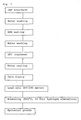
growth chamber 9 of a UHV-CVD device shown in Fig. 6. The loadedSi substrate 8 is supported by a susceptor 12, and then heated by a substrate heater 11. A heater chamber 10 in which the substrate heater 11 is installed, and thegrowth chamber 9 are differentially exhausted by theSi substrate 8 itself, and the respective chambers are exhausted to a vacuum level of 1.3·10-7 to 1.3·10-8 Pa (10-9 to 10-10 Torr) by a turbo-molecular pump 13. Here, a final wet pretreatment of the Si substrate is the DHF treatment, and therefore the surface of the Si substrate remains exposed. In consequence, organic substances in a clean room atmosphere are deposited on the Si substrate during an interval until it is loaded into the UHV-CVD device [Applied Physics A39, p. 73 (1986)]. If the epitaxial growth is carried out, allowing the organic substances (carbon) to remain, a carbon contamination remains in an epitaxial film-Si substrate interface, so that the crystallinity of the epitaxial film noticeably deteriorates and, for example, the deterioration of electric properties such as the backward bias leak current of a pn junction occurs. Thus, after theSi substrate 8 is loaded into thegrowth chamber 9, it is once heated up to a high temperature such as 850°C by the substrate heater 11 and then subjected to hydrogen annealing at this temperature at a vacuum degree of 13 hPa (10 Torr). By this treatment, the above carbon contamination can be removed (The 42nd Applied Physics Related Combination Lecture (1995) Preliminary Manuscript, 29a-Q-8). Afterwards, the temperature is lowered to 800°C or less, and a Si epitaxial growth or a Si1-xGex epitaxial growth is then carried out onto theSi substrate 8 by the use of a gas such as SiH4, Si2H6, GeH4 or B2H6 as a material at a temperature of 600 to 800°C. For example, in the case that a selected Si1-xGex epitaxial film is applied onto a base of a high-speed bipolar transistor, an Si2H6 gas or a GeH4 gas is first used to grow a non-doped selected Si1-xGex epitaxial film, and an Si2H6 gas, a GeH4 gas or a B2H6 gas is then used to grow an in-situ B-doped selected Si1-xGex epitaxial film (so that a parasitic barrier by a Si1-xGex-Si hetero junction may not be formed at a base-collector junction). - When the Si epitaxial growth or the Si1-xGex epitaxial growth is carried out in the above conventional manner, a contamination, particularly boron (B) in the
growth chamber 9 is deposited on the Si substrate during the hydrogen annealing which is carried out immediately before the epitaxial growth. This takes place for the following reason. In the UHV-CVD device, the B2H6 gas or the like is used for the sake of the in-site boron doping into the epitaxial film, but when this gas is introduced into the growth chamber, boron adheres to the inside wall of the growth chamber and it remains thereon. Furthermore, also in the case that the Si substrate already doped with boron at a high concentration is treated, boron vaporizes from the surface of the Si substrate, and it adheres to the inside wall of the growth chamber and remains thereon. Then, when the temperature of the growth chamber becomes higher than 800°C, the remaining boron tends to volatilize from the inside wall of the growth chamber, and it is also deposited on the Si substrate. - If the temperature is lowered, allowing boron to adhere onto the Si substrate and this substrate is then subjected to the epitaxial growth as it is, boron remains in the epitaxial film-Si substrate interface. This has a bad influence on electric properties of devices such as the fluctuation of a threshold voltage in a fine CMOS (because in an n-channel transistor, the threshold voltage is controlled by a boron concentration in a channel section) and the deterioration of a cut-off frequency in a high-speed bipolar transistor using the Si1-xGex epitaxial film as a base (because a parasitic barrier by boron is formed at a base-collector junction).
- The present invention has been developed with the intention of solving these problems, and an object of the present invention is to solve the problem of a carbon contamination in an epitaxial film-Si substrate interface, without allowing boron to remain in the epitaxial film-Si substrate interface.
- That is to say, the present invention is directed to a method for manufacturing a semiconductor device according to
claim 1. - According to the present invention, the problem of the carbon contamination can be solved in the manner that the ion-implanted element or compound reacts during the annealing with the carbon (organic substances) adhered to the surface of the substrate after the removal step of the natural oxide film to vaporize and remove the carbon. In addition, this annealing temperature is set to 800°C or less which is lower than a conventional annealing temperature, and therefore it can be prevented that boron and the like which remain on the inside wall of the CVD device are volatilized therefrom and then deposited on the substrate. That is to say, according to the present invention, boron can be prevented from remaining in the epitaxial film-Si substrate interface, whereby the problem of the carbon contamination in the epitaxial film-Si substrate interface can be solved.
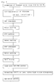
- Fig. 1 is a flow sheet of Example 1.
- Fig. 2 is a flow sheet of Example 2.
- Fig. 3 is a flow sheet of Example 3.
- Fig. 4 shows a dependency of a boron sheet concentration in an epitaxial film-Si substrate interface in a pretreatment method (Examples 1 to 3 and a conventional example).
- Fig. 5 is a sectional view of a high-speed bipolar transistor of a Si1-xGex epitaxial film base which is used in the evaluation of a cut-off frequency.
- In Fig. 5,
- 1 is an emitter N+ type polysilicon,
- 2 is a silicon oxide film,
- 3 is a P+ type polysilicon,
- 4 is a base Si1-xGex layer,
- 5 is a collector N- type epilayer,
- 6 is an N+ layer, and
- 7 is a P- type Si substrate.
-
- Fig. 6 is a schematic view of a UHV-CVD device used in a Si1-xGex epitaxial growth.
- In Fig. 6,
- 8 is an Si substrate,
- 9 is a growth chamber,
- 10 is a heater chamber,
- 11 is a substrate heater,
- 12 is a suscepter,
- 13 is a turbo-molecular pump, and
- 14 is an inlet for a gas such as SiH4, Si2H6, GeH4 or B2H6.
-
- Fig. 7 is a flow sheet of a conventional example.
- An element or a compound which easily reacts with carbon is what easily reacts with carbon at a temperature at the time of annealing. Examples of the element include oxygen, hydrogen and halogens. Examples of the halogens include chlorine, fluorine, bromine and iodine.
- Examples of the compound include compounds of these elements mentioned above, and examples of such compounds include HF, H2O and HCl.
- Above all, oxygen, hydrogen, chlorine and fluorine are preferable, and oxygen, hydrogen and chlorine are most preferable.
- The element or the compound is preferably implanted into a position of the substrate which is not so deep from the surface of the substrate so that it may easily diffuse to the surface at the time of the annealing. This position is within 60 nm preferably within about 25 nm from the surface of the substrate.
- In the present invention, the substrate is usually washed to remove particles and organic substances on the surface of the substrate after the ion-implantation step. This washing is usually accomplished with an ammonia-hydrogen peroxide-pure water mixed agent solution (APM washing) . In general, since Si is exposed on the surface of the substrate before the washing, a natural oxide film is formed on the surface of the substrate by this washing step.
- No particular restriction is put on a removal method of the natural oxide film on the Si substrate, any method can be used, so long as it does not have a bad influence on the substrate. For example, a method using dilute hydrofluoric acid can be used. In addition, a method which is accomplished simultaneously with a next annealing step can also be employed.
- A temperature for the annealing step is in a temperature range in which boron does not volatilize or scarcely volatilizes from the inside wall of a growth chamber of CVD and the ion-implanted element or compound is reacted with carbon (organic substances) on the surface of the substrate. Concretely, the temperature for the annealing step is in the range of 400 to 800°C, preferably 600°C or more.
- A gas which can be used as a material for an epitaxial growth in the present invention is preferably one or more selected from the group consisting of hydrides of Si, Ge and B such as SiH4, Si2H6, GeH4 and B2H6.
- Next, the present invention will be described with reference to drawings.
- Fig. 1 is a flow sheet of Example 1 of the present invention. In the first place, a p-type Si substrate (resistivity = 10 to 20 Ω · cm) having a (100) surface and a diameter of 150 mm was prepared, and a thermal oxide film having a thickness of 10 to 20 nm was formed on this substrate. Next, an oxygen ion was ion-implanted into the substrate under an accelerating energy of 20 keV at a dose of 1014/cm2 to form an oxygen-implanted layer in an extremely shallow region (depth = about 20 nm) in the surface of the Si substrate. Next, a DHF treatment was carried out to etch and remove the thermal oxide film, and after water washing, APM washing was done to remove particles and organic substances from the surface of the substrate. After water washing, another DHF treatment was carried out to remove a natural oxide film on the surface of the Si substrate. Afterwards, an agent solution was washed out by water washing, and finally, the Si substrate was dried by the use of a spin drier. Next, the Si substrate was loaded into a UHV-CVD device shown in Fig. 6.
- The Si substrate was set to a susceptor 12, and then heated, for example, up to 750°C at a temperature of 800°C or less by the use of a substrate heater 11. At this time, a base pressure was at a level of about 1.3·10-7 Pa (10-9 Torr). Immediately after the Si substrate was maintained at this temperature for about 10 minutes, the temperature was lowered to 700°C, and an Si epitaxial film having a thickness of 200 nm was formed by the use of an Si2H6 gas. Afterward, the Si substrate was taken out, and a contamination amount of carbon (C) and boron (B) in an Si epitaxial film-Si substrate interface was measured by the use of SIMS. According to the results measured by the SIMS, the C contamination in the interface was not confirmed in this example as in the case of a conventional example in accordance with a flow sheet shown in Fig. 7. This fact of the example would be due to that oxygen diffuses from the oxygen-implanted layer formed on the surface of the Si substrate into the surface of the Si substrate at the ultra high vacuum annealing at 750°C, and this oxygen reacts with C in the surface of the Si substrate to form CO and CO2 and they then volatilize from the surface of the Si substrate. It has been found that if the oxygen-implanted layer is formed in the vicinity of the surface of the substrate, the diffusion of oxygen into the surface of the Si substrate sufficiently occurs even at about 750°C, and in consequence, the C contamination on the DHF-treated Si substrate surface can easily be removed.
- The results of the B (boron) contamination are shown in Fig. 4. That is to say, in this example, the B contamination was about 1011/cm2 in terms of a sheet concentration, and this contamination amount was as low as 1/10 of a conventional example in which the B contamination was about 1012/cm2. This fact of the example was due to that the annealing before the growth step was done at a low temperature of 750°C, and so the volatilization of B which adhered to the inside wall of the growth chamber was much more restrained as compared with the annealing at 850°C in the conventional example.
- Next, electric properties of devices were inspected to evaluate the effects of the B contamination reduction in the interface.
- Fig. 5 is a sectional view of a high-speed bipolar transistor of a Si1-xGex epitaxial film base which is used in the evaluation of a cut-off frequency. On each p- type (100) Si substrate (resistivity = 10 to 20 Ω · cm) 7, an N+ layer 6, a collector N- epitaxial layer 5, a
silicon oxide film 2 and a p+ type polysilicon 3 were formed, and a non-doped Si1-xGex epitaxial film and in-situ B-doped Si1-xGex epitaxial base growth was carried out in accordance with the flow sheets of this example and the conventional example. After the growth, an emitter N+ type polysilicon 1 was formed. In accordance with the procedures of this example and the conventional example, high-speed bipolar transistors of the Si1-xGex epitaxial film bases were formed, and a collector current dependency at a cut-off frequency in each high-speed bipolar transistor was then measured. According to the measured results, a maximum cut-off frequency ft was about 40 GHz in the conventional example, but in this example, it was improved to about 60 GHz. This effect is due to that the B contamination of in the epitaxial film-substrate interface can be remarkably restrained as described above. - Next, a second example of the present invention will be described.
- Fig. 2 is a flow sheet of Example 2 of the present invention. A Si substrate used herein was the same as in Example 1. The same procedure as in Example 1 was conducted except that hydrogen was ion-implanted in place of oxygen. According to the results measured by an SIMS, any C contamination in an epitaxial film-Si substrate interface was not confirmed in this example. This fact would be due to that hydrogen diffuses from a hydrogen-implanted layer formed on the surface of the Si substrate into the surface of the Si substrate at an ultra high vacuum annealing at 750°C, and this hydrogen reacts with C in the surface of the Si substrate to form hydrocarbons and the like and they then volatilize from the surface of the Si substrate. It has been found that if the hydrogen-implanted layer is formed in the vicinity of the surface of the substrate, the diffusion of hydrogen to the surface of the Si substrate sufficiently occurs even at about 750°C, and in consequence, the C contamination on the DHF-treated Si substrate surface can easily be removed.
- As shown in Fig. 4, a B sheet concentration in the interface in this example was about 1011/cm2, and so the B contamination in the interface could be restrained to about 1/10 of a conventional example. This fact is due to that, as in Example 1, the annealing before the growth was carried out at a low temperature of 750°C, and so the volatilization of B which adhered to the inside wall of a growth chamber was much more restrained as compared with the annealing at 850°C in the conventional example.
- Furthermore, also in this example, a bipolar transistor shown in Fig. 5 was experimentally made as in Example 1, and electric properties of the transistor were evaluated. According to the evaluated results, a maximum cut-off frequency ft in the high-speed bipolar transistor of a Si1-xGex epitaxial film base made by the procedure of this example was about 60 GHz as in Example 1, which meant that the ft value could be much more improved owing to the restraint of the B contamination in the interface than in the conventional example.
- Next, a third example of the present invention will be described.
- Fig. 3 is a flow sheet of Example 3 of the present invention. An Si substrate used herein was the same as in Example 1 or 2. The same procedure as in Example 1 or 2 was conducted except that chlorine was ion-implanted in place of oxygen or hydrogen. According to the results measured by SIMS, any C contamination in an epitaxial film-Si substrate interface was not confirmed in this example. This fact would be due to that chlorine diffuses from a chlorine-implanted layer formed on the surface of the Si substrate to the surface of the Si substrate at an ultra high vacuum annealing at 750°C, and this chlorine reacts with C in the surface of the Si substrate to form chlorides of carbon and the like and they then volatilize from the surface of the Si substrate. If the chlorine-implanted layer is formed in the vicinity of the surface of the substrate, the diffusion of chlorine to the surface of the Si substrate sufficiently occurs even at about 750°C, and in consequence, the C contamination on the DHF-treated Si substrate surface can easily be removed.
- As shown in Fig. 4, a B sheet concentration in the interface in this example was about 1011/cm2, and so the B contamination in the interface could be restrained to about 1/10 of a conventional example. This fact is due to that, as in Example 1 or 2, the annealing before the growth was carried out at a low temperature of 750°C, and so the volatilization of B which adhered to the inside wall of a growth chamber was much more restrained as compared with the annealing at 850°C in the conventional example.
- Furthermore, also in this example, a bipolar transistor shown in Fig. 5 was experimentally made as in Example 1 or 2, and electric properties of the transistor were evaluated. According to the evaluated results, a maximum cut-off frequency ft in the high-speed bipolar transistor of a Si1-xGex epitaxial film base made by the procedure of this example was about 60 GHz as in Example 1 or 2, which meant that the ft value could be much more improved owing to the restraint of the B contamination in the interface than in the conventional example.
- According to the present invention, an epitaxial film can be formed which is free from contamination with carbon in an interface between an epitaxial film and an Si substrate and an element (e.g., B) which adheres to the inside wall of a
growth chamber 9 in a UHV-CVD device. As a result, there can be obtained an effect of remarkably improving electric properties such as a leak current in a diffusion layer of a fine CMOS, the fluctuation of a threshold voltage, a junction leak between a base and a collector in a high-speed bipolar transistor of a Si1-xGex epitaxial film base and cut-off frequency.
Claims (6)
- A method of manufacturing a semiconductor device comprising the steps in sequence of:a) ion-implanting, into a Si substrate, an element or a compound which reacts with carbon in a later annealing step,b) washing the Si substrate from step (a) to remove particles and organic substances remaining on the Si substrate after the ion-implanting step, said washing resulting in the formation of a natural oxide film on the Si substrate,c) removing the natural oxide film on the Si substrate,d) annealing the Si substrate, which has been subjected to the ion-implantation of step a) the washing of step b) and the removal of the natural oxide film of steps c) at a temperature of 800° or less in a CVD device; ande) carrying out Si epitaxial growth or Si1-xGex epitaxial growth on the annealed substrate of step d) in the CVD device.
- The method for manufacturing a semiconductor device according to claim 1, wherein the washing of step b) uses an ammonia-hydrogen peroxide pure water solution.
- The method for manufacturing a semiconductor device according to Claim 1 or 2, wherein the element or the compound which reacts with carbon in step d) is an element or a compound selected from the group consisting of oxygen, hydrogen, halogens and compounds thereof.
- The method for manufacturing a semiconductor device according to Claim 3, wherein the halogen is chlorine.
- The method for manufacturing a semiconductor device according to Claim 1, wherein the epitaxial growth by the CVD device is accomplished by using, as a material, one or more selected from the group consisting of hydrides of Si, Ge and B.
- The method for manufacturing a semiconductor device according to claim 5, wherein the epitaxial growth uses SiH4, Si2H6, GeH4 and/or B2H6.
Applications Claiming Priority (3)
| Application Number | Priority Date | Filing Date | Title |
|---|---|---|---|
| JP120131/96 | 1996-05-15 | ||
| JP8120131A JP2836576B2 (en) | 1996-05-15 | 1996-05-15 | Method for manufacturing semiconductor device |
| JP12013196 | 1996-05-15 |
Publications (3)
| Publication Number | Publication Date |
|---|---|
| EP0813232A2 EP0813232A2 (en) | 1997-12-17 |
| EP0813232A3 EP0813232A3 (en) | 1998-09-02 |
| EP0813232B1 true EP0813232B1 (en) | 2002-09-25 |
Family
ID=14778747
Family Applications (1)
| Application Number | Title | Priority Date | Filing Date |
|---|---|---|---|
| EP97107876A Expired - Lifetime EP0813232B1 (en) | 1996-05-15 | 1997-05-14 | Method of reducing the amount of carbon in an interface between an epitaxial film and a Si substrate |
Country Status (4)
| Country | Link |
|---|---|
| US (1) | US5920795A (en) |
| EP (1) | EP0813232B1 (en) |
| JP (1) | JP2836576B2 (en) |
| DE (1) | DE69715735T2 (en) |
Families Citing this family (7)
| Publication number | Priority date | Publication date | Assignee | Title |
|---|---|---|---|---|
| FR2774509B1 (en) * | 1998-01-30 | 2001-11-16 | Sgs Thomson Microelectronics | METHOD FOR DEPOSITING A REGION OF SINGLE CRYSTAL SILICON |
| US6143073A (en) * | 1998-11-19 | 2000-11-07 | Heraeus Shin-Etsu America | Methods and apparatus for minimizing white point defects in quartz glass crucibles |
| WO2001033618A1 (en) * | 1999-10-29 | 2001-05-10 | Matsushita Electric Industrial Co., Ltd. | Method for cleaning substrate and method for manufacturing semiconductor device |
| US6406929B1 (en) | 2000-06-21 | 2002-06-18 | University Of Vermont And State Agricultural College | Structure and method for abrupt PN junction diode formed using chemical vapor deposition processing |
| JP2003086554A (en) * | 2001-09-11 | 2003-03-20 | Mitsubishi Heavy Ind Ltd | Apparatus and method for manufacturing semiconductor substrate |
| KR100678468B1 (en) * | 2005-01-14 | 2007-02-02 | 삼성전자주식회사 | In-situ cleaning method of semiconductor substrate and manufacturing method of semiconductor device employing same |
| KR100632460B1 (en) * | 2005-02-03 | 2006-10-11 | 삼성전자주식회사 | Manufacturing Method of Semiconductor Device |
Family Cites Families (9)
| Publication number | Priority date | Publication date | Assignee | Title |
|---|---|---|---|---|
| JPH0644562B2 (en) * | 1985-05-24 | 1994-06-08 | 日本電気株式会社 | Surface cleaning method |
| JP2595935B2 (en) * | 1985-12-13 | 1997-04-02 | 日本電気株式会社 | Surface cleaning method |
| US4717681A (en) * | 1986-05-19 | 1988-01-05 | Texas Instruments Incorporated | Method of making a heterojunction bipolar transistor with SIPOS |
| JPS6348817A (en) * | 1986-08-19 | 1988-03-01 | Fujitsu Ltd | Epitaxial growth method |
| JPS6351641A (en) * | 1986-08-21 | 1988-03-04 | Oki Electric Ind Co Ltd | Fine pattern formation of single crystal or polycrystalline si film |
| JPS6410616A (en) * | 1987-07-02 | 1989-01-13 | Nec Corp | Method and device for growth of compound semiconductor crystal |
| JPS6423538A (en) * | 1987-07-20 | 1989-01-26 | Nec Corp | Method and equipment for manufacturing semiconductor device |
| JPH04304635A (en) * | 1991-04-01 | 1992-10-28 | Hitachi Ltd | Semiconductor manufacturing method and device with substrate cleaning device |
| US5516710A (en) * | 1994-11-10 | 1996-05-14 | Northern Telecom Limited | Method of forming a transistor |
-
1996
- 1996-05-15 JP JP8120131A patent/JP2836576B2/en not_active Expired - Fee Related
-
1997
- 1997-05-05 US US08/851,366 patent/US5920795A/en not_active Expired - Lifetime
- 1997-05-14 DE DE69715735T patent/DE69715735T2/en not_active Expired - Fee Related
- 1997-05-14 EP EP97107876A patent/EP0813232B1/en not_active Expired - Lifetime
Also Published As
| Publication number | Publication date |
|---|---|
| US5920795A (en) | 1999-07-06 |
| EP0813232A3 (en) | 1998-09-02 |
| JPH09306847A (en) | 1997-11-28 |
| EP0813232A2 (en) | 1997-12-17 |
| JP2836576B2 (en) | 1998-12-14 |
| DE69715735T2 (en) | 2003-05-22 |
| DE69715735D1 (en) | 2002-10-31 |
Similar Documents
| Publication | Publication Date | Title |
|---|---|---|
| EP0090940B1 (en) | Method of forming emitter and intrinsic base regions of a bipolar transistor | |
| US5821158A (en) | Substrate surface treatment method capable of removing a spontaneous oxide film at a relatively low temperature | |
| US5731626A (en) | Process for controlling dopant diffusion in a semiconductor layer and semiconductor layer formed thereby | |
| US6368927B1 (en) | Method of manufacturing transistor having elevated source and drain regions | |
| KR100678468B1 (en) | In-situ cleaning method of semiconductor substrate and manufacturing method of semiconductor device employing same | |
| JP3079575B2 (en) | Method for manufacturing semiconductor device | |
| US6358865B2 (en) | Oxidation of silicon using fluorine implant | |
| US5565690A (en) | Method for doping strained heterojunction semiconductor devices and structure | |
| EP0813232B1 (en) | Method of reducing the amount of carbon in an interface between an epitaxial film and a Si substrate | |
| JPH0684819A (en) | Method for producing highly doped semiconductor material | |
| US6365473B1 (en) | Method of manufacturing a transistor in a semiconductor device | |
| US6228166B1 (en) | Method for boron contamination reduction in IC fabrication | |
| US7556048B2 (en) | In-situ removal of surface impurities prior to arsenic-doped polysilicon deposition in the fabrication of a heterojunction bipolar transistor | |
| US5674777A (en) | Method for forming silicon-boron binary compound layer as boron diffusion source in silicon electronic device | |
| US6703283B1 (en) | Discontinuous dielectric interface for bipolar transistors | |
| JP2920546B2 (en) | Method for manufacturing same-polarity gate MIS transistor | |
| KR100333727B1 (en) | Method for fabricating MOSFET with elevated source/drain structure | |
| JP2973949B2 (en) | Method for manufacturing semiconductor device | |
| EP1052685A2 (en) | Integrated circuit device having a fluorine implanted oxide layer | |
| Donahue et al. | Low Temperature Silicon Epitaxy Deposited by Very Low Pressure Chemical Vapor Deposition: II. Autodoping | |
| Kiyota et al. | Reduction of base resistance and increase in cutoff frequency of Si bipolar transistor using rapid vapor-phase doping | |
| JP2956616B2 (en) | Method for manufacturing semiconductor device | |
| Topich | Reduction of Defects in Ion Implanted Bipolar Transistors by Argon Back Side Damage | |
| Theunissen et al. | Boron Vapour Phase Doping of Silicon for Bipolar Device Applications | |
| KR100269716B1 (en) | A method for boron contamination reduction in ic fabrication |
Legal Events
| Date | Code | Title | Description |
|---|---|---|---|
| PUAI | Public reference made under article 153(3) epc to a published international application that has entered the european phase |
Free format text: ORIGINAL CODE: 0009012 |
|
| AK | Designated contracting states |
Kind code of ref document: A2 Designated state(s): DE FR GB |
|
| PUAL | Search report despatched |
Free format text: ORIGINAL CODE: 0009013 |
|
| AK | Designated contracting states |
Kind code of ref document: A3 Designated state(s): DE FR GB |
|
| 17P | Request for examination filed |
Effective date: 19980729 |
|
| 17Q | First examination report despatched |
Effective date: 19991201 |
|
| GRAG | Despatch of communication of intention to grant |
Free format text: ORIGINAL CODE: EPIDOS AGRA |
|
| GRAG | Despatch of communication of intention to grant |
Free format text: ORIGINAL CODE: EPIDOS AGRA |
|
| GRAH | Despatch of communication of intention to grant a patent |
Free format text: ORIGINAL CODE: EPIDOS IGRA |
|
| GRAH | Despatch of communication of intention to grant a patent |
Free format text: ORIGINAL CODE: EPIDOS IGRA |
|
| GRAA | (expected) grant |
Free format text: ORIGINAL CODE: 0009210 |
|
| AK | Designated contracting states |
Kind code of ref document: B1 Designated state(s): DE FR GB |
|
| REG | Reference to a national code |
Ref country code: GB Ref legal event code: FG4D |
|
| REF | Corresponds to: |
Ref document number: 69715735 Country of ref document: DE Date of ref document: 20021031 |
|
| ET | Fr: translation filed | ||
| RAP2 | Party data changed (patent owner data changed or rights of a patent transferred) |
Owner name: NEC ELECTRONICS CORPORATION |
|
| PLBE | No opposition filed within time limit |
Free format text: ORIGINAL CODE: 0009261 |
|
| STAA | Information on the status of an ep patent application or granted ep patent |
Free format text: STATUS: NO OPPOSITION FILED WITHIN TIME LIMIT |
|
| REG | Reference to a national code |
Ref country code: GB Ref legal event code: 732E |
|
| 26N | No opposition filed |
Effective date: 20030626 |
|
| REG | Reference to a national code |
Ref country code: FR Ref legal event code: TP |
|
| PGFP | Annual fee paid to national office [announced via postgrant information from national office to epo] |
Ref country code: FR Payment date: 20040510 Year of fee payment: 8 |
|
| PGFP | Annual fee paid to national office [announced via postgrant information from national office to epo] |
Ref country code: GB Payment date: 20040512 Year of fee payment: 8 |
|
| PGFP | Annual fee paid to national office [announced via postgrant information from national office to epo] |
Ref country code: DE Payment date: 20040527 Year of fee payment: 8 |
|
| PG25 | Lapsed in a contracting state [announced via postgrant information from national office to epo] |
Ref country code: GB Free format text: LAPSE BECAUSE OF NON-PAYMENT OF DUE FEES Effective date: 20050514 |
|
| PG25 | Lapsed in a contracting state [announced via postgrant information from national office to epo] |
Ref country code: DE Free format text: LAPSE BECAUSE OF NON-PAYMENT OF DUE FEES Effective date: 20051201 |
|
| GBPC | Gb: european patent ceased through non-payment of renewal fee |
Effective date: 20050514 |
|
| PG25 | Lapsed in a contracting state [announced via postgrant information from national office to epo] |
Ref country code: FR Free format text: LAPSE BECAUSE OF NON-PAYMENT OF DUE FEES Effective date: 20060131 |
|
| REG | Reference to a national code |
Ref country code: FR Ref legal event code: ST Effective date: 20060131 |