US6703283B1 - Discontinuous dielectric interface for bipolar transistors - Google Patents
Discontinuous dielectric interface for bipolar transistors Download PDFInfo
- Publication number
- US6703283B1 US6703283B1 US09/244,958 US24495899A US6703283B1 US 6703283 B1 US6703283 B1 US 6703283B1 US 24495899 A US24495899 A US 24495899A US 6703283 B1 US6703283 B1 US 6703283B1
- Authority
- US
- United States
- Prior art keywords
- region
- semiconductor material
- process according
- semiconductor
- dielectric material
- Prior art date
- Legal status (The legal status is an assumption and is not a legal conclusion. Google has not performed a legal analysis and makes no representation as to the accuracy of the status listed.)
- Expired - Lifetime
Links
- 238000000034 method Methods 0.000 claims abstract description 128
- 239000004065 semiconductor Substances 0.000 claims abstract description 118
- 239000000463 material Substances 0.000 claims abstract description 82
- 239000003989 dielectric material Substances 0.000 claims abstract description 65
- IJGRMHOSHXDMSA-UHFFFAOYSA-N Atomic nitrogen Chemical compound N#N IJGRMHOSHXDMSA-UHFFFAOYSA-N 0.000 claims abstract description 36
- 229910052757 nitrogen Inorganic materials 0.000 claims abstract description 18
- 239000010410 layer Substances 0.000 claims description 40
- 229910021421 monocrystalline silicon Inorganic materials 0.000 claims description 40
- 229910021420 polycrystalline silicon Inorganic materials 0.000 claims description 38
- 239000007789 gas Substances 0.000 claims description 24
- XUIMIQQOPSSXEZ-UHFFFAOYSA-N Silicon Chemical compound [Si] XUIMIQQOPSSXEZ-UHFFFAOYSA-N 0.000 claims description 19
- 229910052710 silicon Inorganic materials 0.000 claims description 19
- 239000010703 silicon Substances 0.000 claims description 19
- 238000000151 deposition Methods 0.000 claims description 11
- 230000008021 deposition Effects 0.000 claims description 9
- 239000002356 single layer Substances 0.000 claims description 9
- 229910052581 Si3N4 Inorganic materials 0.000 claims description 7
- 229910021417 amorphous silicon Inorganic materials 0.000 claims description 7
- QJGQUHMNIGDVPM-UHFFFAOYSA-N nitrogen group Chemical group [N] QJGQUHMNIGDVPM-UHFFFAOYSA-N 0.000 claims description 7
- HQVNEWCFYHHQES-UHFFFAOYSA-N silicon nitride Chemical compound N12[Si]34N5[Si]62N3[Si]51N64 HQVNEWCFYHHQES-UHFFFAOYSA-N 0.000 claims description 7
- 229910000577 Silicon-germanium Inorganic materials 0.000 claims description 6
- 229910020776 SixNy Inorganic materials 0.000 claims description 4
- 229910020781 SixOy Inorganic materials 0.000 claims description 2
- 125000004433 nitrogen atom Chemical group N* 0.000 claims description 2
- 230000003647 oxidation Effects 0.000 description 30
- 238000007254 oxidation reaction Methods 0.000 description 30
- 239000000758 substrate Substances 0.000 description 28
- 235000012431 wafers Nutrition 0.000 description 22
- 229920005591 polysilicon Polymers 0.000 description 20
- 238000005229 chemical vapour deposition Methods 0.000 description 18
- VYPSYNLAJGMNEJ-UHFFFAOYSA-N Silicium dioxide Chemical compound O=[Si]=O VYPSYNLAJGMNEJ-UHFFFAOYSA-N 0.000 description 7
- QVGXLLKOCUKJST-UHFFFAOYSA-N atomic oxygen Chemical compound [O] QVGXLLKOCUKJST-UHFFFAOYSA-N 0.000 description 7
- 229910052760 oxygen Inorganic materials 0.000 description 7
- 239000001301 oxygen Substances 0.000 description 7
- 229940110728 nitrogen / oxygen Drugs 0.000 description 5
- QGZKDVFQNNGYKY-UHFFFAOYSA-N Ammonia Chemical compound N QGZKDVFQNNGYKY-UHFFFAOYSA-N 0.000 description 4
- 125000004429 atom Chemical group 0.000 description 4
- 230000015572 biosynthetic process Effects 0.000 description 4
- 238000012986 modification Methods 0.000 description 4
- 230000004048 modification Effects 0.000 description 4
- 239000007943 implant Substances 0.000 description 3
- 238000004518 low pressure chemical vapour deposition Methods 0.000 description 3
- 239000000203 mixture Substances 0.000 description 3
- 229910000069 nitrogen hydride Inorganic materials 0.000 description 3
- 235000012239 silicon dioxide Nutrition 0.000 description 3
- 229910007991 Si-N Inorganic materials 0.000 description 2
- 229910006294 Si—N Inorganic materials 0.000 description 2
- 238000004140 cleaning Methods 0.000 description 2
- 239000013078 crystal Substances 0.000 description 2
- 229910021419 crystalline silicon Inorganic materials 0.000 description 2
- 230000007547 defect Effects 0.000 description 2
- MROCJMGDEKINLD-UHFFFAOYSA-N dichlorosilane Chemical compound Cl[SiH2]Cl MROCJMGDEKINLD-UHFFFAOYSA-N 0.000 description 2
- 238000002513 implantation Methods 0.000 description 2
- 238000004519 manufacturing process Methods 0.000 description 2
- 150000004767 nitrides Chemical class 0.000 description 2
- 238000000623 plasma-assisted chemical vapour deposition Methods 0.000 description 2
- 239000010453 quartz Substances 0.000 description 2
- 239000000377 silicon dioxide Substances 0.000 description 2
- BLRPTPMANUNPDV-UHFFFAOYSA-N Silane Chemical compound [SiH4] BLRPTPMANUNPDV-UHFFFAOYSA-N 0.000 description 1
- UMVBXBACMIOFDO-UHFFFAOYSA-N [N].[Si] Chemical compound [N].[Si] UMVBXBACMIOFDO-UHFFFAOYSA-N 0.000 description 1
- 238000010923 batch production Methods 0.000 description 1
- 230000000740 bleeding effect Effects 0.000 description 1
- 239000000919 ceramic Substances 0.000 description 1
- 238000006243 chemical reaction Methods 0.000 description 1
- 229910052681 coesite Inorganic materials 0.000 description 1
- 238000001816 cooling Methods 0.000 description 1
- 229910052906 cristobalite Inorganic materials 0.000 description 1
- 238000002425 crystallisation Methods 0.000 description 1
- 230000008025 crystallization Effects 0.000 description 1
- 230000007423 decrease Effects 0.000 description 1
- 238000005137 deposition process Methods 0.000 description 1
- 230000000694 effects Effects 0.000 description 1
- 239000012777 electrically insulating material Substances 0.000 description 1
- 238000005516 engineering process Methods 0.000 description 1
- 238000005530 etching Methods 0.000 description 1
- 238000011065 in-situ storage Methods 0.000 description 1
- 239000011261 inert gas Substances 0.000 description 1
- 239000011810 insulating material Substances 0.000 description 1
- 230000014759 maintenance of location Effects 0.000 description 1
- 230000001590 oxidative effect Effects 0.000 description 1
- 230000009467 reduction Effects 0.000 description 1
- 229910000077 silane Inorganic materials 0.000 description 1
- 229910052814 silicon oxide Inorganic materials 0.000 description 1
- 229910052682 stishovite Inorganic materials 0.000 description 1
- 239000013589 supplement Substances 0.000 description 1
- 229910052905 tridymite Inorganic materials 0.000 description 1
Images


Classifications
-
- H—ELECTRICITY
- H01—ELECTRIC ELEMENTS
- H01L—SEMICONDUCTOR DEVICES NOT COVERED BY CLASS H10
- H01L21/00—Processes or apparatus adapted for the manufacture or treatment of semiconductor or solid state devices or of parts thereof
- H01L21/02—Manufacture or treatment of semiconductor devices or of parts thereof
- H01L21/04—Manufacture or treatment of semiconductor devices or of parts thereof the devices having potential barriers, e.g. a PN junction, depletion layer or carrier concentration layer
- H01L21/18—Manufacture or treatment of semiconductor devices or of parts thereof the devices having potential barriers, e.g. a PN junction, depletion layer or carrier concentration layer the devices having semiconductor bodies comprising elements of Group IV of the Periodic Table or AIIIBV compounds with or without impurities, e.g. doping materials
-
- H—ELECTRICITY
- H01—ELECTRIC ELEMENTS
- H01L—SEMICONDUCTOR DEVICES NOT COVERED BY CLASS H10
- H01L21/00—Processes or apparatus adapted for the manufacture or treatment of semiconductor or solid state devices or of parts thereof
- H01L21/02—Manufacture or treatment of semiconductor devices or of parts thereof
- H01L21/02104—Forming layers
- H01L21/02107—Forming insulating materials on a substrate
- H01L21/02109—Forming insulating materials on a substrate characterised by the type of layer, e.g. type of material, porous/non-porous, pre-cursors, mixtures or laminates
- H01L21/02112—Forming insulating materials on a substrate characterised by the type of layer, e.g. type of material, porous/non-porous, pre-cursors, mixtures or laminates characterised by the material of the layer
- H01L21/02123—Forming insulating materials on a substrate characterised by the type of layer, e.g. type of material, porous/non-porous, pre-cursors, mixtures or laminates characterised by the material of the layer the material containing silicon
- H01L21/0217—Forming insulating materials on a substrate characterised by the type of layer, e.g. type of material, porous/non-porous, pre-cursors, mixtures or laminates characterised by the material of the layer the material containing silicon the material being a silicon nitride not containing oxygen, e.g. SixNy or SixByNz
-
- H—ELECTRICITY
- H01—ELECTRIC ELEMENTS
- H01L—SEMICONDUCTOR DEVICES NOT COVERED BY CLASS H10
- H01L21/00—Processes or apparatus adapted for the manufacture or treatment of semiconductor or solid state devices or of parts thereof
- H01L21/02—Manufacture or treatment of semiconductor devices or of parts thereof
- H01L21/02104—Forming layers
- H01L21/02107—Forming insulating materials on a substrate
- H01L21/02109—Forming insulating materials on a substrate characterised by the type of layer, e.g. type of material, porous/non-porous, pre-cursors, mixtures or laminates
- H01L21/02112—Forming insulating materials on a substrate characterised by the type of layer, e.g. type of material, porous/non-porous, pre-cursors, mixtures or laminates characterised by the material of the layer
- H01L21/02123—Forming insulating materials on a substrate characterised by the type of layer, e.g. type of material, porous/non-porous, pre-cursors, mixtures or laminates characterised by the material of the layer the material containing silicon
- H01L21/02126—Forming insulating materials on a substrate characterised by the type of layer, e.g. type of material, porous/non-porous, pre-cursors, mixtures or laminates characterised by the material of the layer the material containing silicon the material containing Si, O, and at least one of H, N, C, F, or other non-metal elements, e.g. SiOC, SiOC:H or SiONC
- H01L21/0214—Forming insulating materials on a substrate characterised by the type of layer, e.g. type of material, porous/non-porous, pre-cursors, mixtures or laminates characterised by the material of the layer the material containing silicon the material containing Si, O, and at least one of H, N, C, F, or other non-metal elements, e.g. SiOC, SiOC:H or SiONC the material being a silicon oxynitride, e.g. SiON or SiON:H
-
- H—ELECTRICITY
- H01—ELECTRIC ELEMENTS
- H01L—SEMICONDUCTOR DEVICES NOT COVERED BY CLASS H10
- H01L21/00—Processes or apparatus adapted for the manufacture or treatment of semiconductor or solid state devices or of parts thereof
- H01L21/02—Manufacture or treatment of semiconductor devices or of parts thereof
- H01L21/02104—Forming layers
- H01L21/02107—Forming insulating materials on a substrate
- H01L21/02225—Forming insulating materials on a substrate characterised by the process for the formation of the insulating layer
- H01L21/02227—Forming insulating materials on a substrate characterised by the process for the formation of the insulating layer formation by a process other than a deposition process
- H01L21/02247—Forming insulating materials on a substrate characterised by the process for the formation of the insulating layer formation by a process other than a deposition process formation by nitridation, e.g. nitridation of the substrate
-
- H—ELECTRICITY
- H01—ELECTRIC ELEMENTS
- H01L—SEMICONDUCTOR DEVICES NOT COVERED BY CLASS H10
- H01L21/00—Processes or apparatus adapted for the manufacture or treatment of semiconductor or solid state devices or of parts thereof
- H01L21/02—Manufacture or treatment of semiconductor devices or of parts thereof
- H01L21/02104—Forming layers
- H01L21/02107—Forming insulating materials on a substrate
- H01L21/02225—Forming insulating materials on a substrate characterised by the process for the formation of the insulating layer
- H01L21/02227—Forming insulating materials on a substrate characterised by the process for the formation of the insulating layer formation by a process other than a deposition process
- H01L21/02249—Forming insulating materials on a substrate characterised by the process for the formation of the insulating layer formation by a process other than a deposition process formation by combined oxidation and nitridation performed simultaneously
-
- H—ELECTRICITY
- H01—ELECTRIC ELEMENTS
- H01L—SEMICONDUCTOR DEVICES NOT COVERED BY CLASS H10
- H01L21/00—Processes or apparatus adapted for the manufacture or treatment of semiconductor or solid state devices or of parts thereof
- H01L21/02—Manufacture or treatment of semiconductor devices or of parts thereof
- H01L21/02104—Forming layers
- H01L21/02107—Forming insulating materials on a substrate
- H01L21/02225—Forming insulating materials on a substrate characterised by the process for the formation of the insulating layer
- H01L21/02227—Forming insulating materials on a substrate characterised by the process for the formation of the insulating layer formation by a process other than a deposition process
- H01L21/02255—Forming insulating materials on a substrate characterised by the process for the formation of the insulating layer formation by a process other than a deposition process formation by thermal treatment
-
- H—ELECTRICITY
- H01—ELECTRIC ELEMENTS
- H01L—SEMICONDUCTOR DEVICES NOT COVERED BY CLASS H10
- H01L21/00—Processes or apparatus adapted for the manufacture or treatment of semiconductor or solid state devices or of parts thereof
- H01L21/02—Manufacture or treatment of semiconductor devices or of parts thereof
- H01L21/04—Manufacture or treatment of semiconductor devices or of parts thereof the devices having potential barriers, e.g. a PN junction, depletion layer or carrier concentration layer
- H01L21/18—Manufacture or treatment of semiconductor devices or of parts thereof the devices having potential barriers, e.g. a PN junction, depletion layer or carrier concentration layer the devices having semiconductor bodies comprising elements of Group IV of the Periodic Table or AIIIBV compounds with or without impurities, e.g. doping materials
- H01L21/30—Treatment of semiconductor bodies using processes or apparatus not provided for in groups H01L21/20 - H01L21/26
- H01L21/31—Treatment of semiconductor bodies using processes or apparatus not provided for in groups H01L21/20 - H01L21/26 to form insulating layers thereon, e.g. for masking or by using photolithographic techniques; After treatment of these layers; Selection of materials for these layers
- H01L21/314—Inorganic layers
- H01L21/3143—Inorganic layers composed of alternated layers or of mixtures of nitrides and oxides or of oxinitrides, e.g. formation of oxinitride by oxidation of nitride layers
- H01L21/3144—Inorganic layers composed of alternated layers or of mixtures of nitrides and oxides or of oxinitrides, e.g. formation of oxinitride by oxidation of nitride layers on silicon
-
- H—ELECTRICITY
- H01—ELECTRIC ELEMENTS
- H01L—SEMICONDUCTOR DEVICES NOT COVERED BY CLASS H10
- H01L21/00—Processes or apparatus adapted for the manufacture or treatment of semiconductor or solid state devices or of parts thereof
- H01L21/02—Manufacture or treatment of semiconductor devices or of parts thereof
- H01L21/04—Manufacture or treatment of semiconductor devices or of parts thereof the devices having potential barriers, e.g. a PN junction, depletion layer or carrier concentration layer
- H01L21/18—Manufacture or treatment of semiconductor devices or of parts thereof the devices having potential barriers, e.g. a PN junction, depletion layer or carrier concentration layer the devices having semiconductor bodies comprising elements of Group IV of the Periodic Table or AIIIBV compounds with or without impurities, e.g. doping materials
- H01L21/30—Treatment of semiconductor bodies using processes or apparatus not provided for in groups H01L21/20 - H01L21/26
- H01L21/31—Treatment of semiconductor bodies using processes or apparatus not provided for in groups H01L21/20 - H01L21/26 to form insulating layers thereon, e.g. for masking or by using photolithographic techniques; After treatment of these layers; Selection of materials for these layers
- H01L21/314—Inorganic layers
- H01L21/318—Inorganic layers composed of nitrides
- H01L21/3185—Inorganic layers composed of nitrides of siliconnitrides
-
- H—ELECTRICITY
- H01—ELECTRIC ELEMENTS
- H01L—SEMICONDUCTOR DEVICES NOT COVERED BY CLASS H10
- H01L29/00—Semiconductor devices specially adapted for rectifying, amplifying, oscillating or switching and having potential barriers; Capacitors or resistors having potential barriers, e.g. a PN-junction depletion layer or carrier concentration layer; Details of semiconductor bodies or of electrodes thereof ; Multistep manufacturing processes therefor
- H01L29/02—Semiconductor bodies ; Multistep manufacturing processes therefor
- H01L29/06—Semiconductor bodies ; Multistep manufacturing processes therefor characterised by their shape; characterised by the shapes, relative sizes, or dispositions of the semiconductor regions ; characterised by the concentration or distribution of impurities within semiconductor regions
- H01L29/08—Semiconductor bodies ; Multistep manufacturing processes therefor characterised by their shape; characterised by the shapes, relative sizes, or dispositions of the semiconductor regions ; characterised by the concentration or distribution of impurities within semiconductor regions with semiconductor regions connected to an electrode carrying current to be rectified, amplified or switched and such electrode being part of a semiconductor device which comprises three or more electrodes
- H01L29/0804—Emitter regions of bipolar transistors
-
- H—ELECTRICITY
- H01—ELECTRIC ELEMENTS
- H01L—SEMICONDUCTOR DEVICES NOT COVERED BY CLASS H10
- H01L29/00—Semiconductor devices specially adapted for rectifying, amplifying, oscillating or switching and having potential barriers; Capacitors or resistors having potential barriers, e.g. a PN-junction depletion layer or carrier concentration layer; Details of semiconductor bodies or of electrodes thereof ; Multistep manufacturing processes therefor
- H01L29/02—Semiconductor bodies ; Multistep manufacturing processes therefor
- H01L29/06—Semiconductor bodies ; Multistep manufacturing processes therefor characterised by their shape; characterised by the shapes, relative sizes, or dispositions of the semiconductor regions ; characterised by the concentration or distribution of impurities within semiconductor regions
- H01L29/08—Semiconductor bodies ; Multistep manufacturing processes therefor characterised by their shape; characterised by the shapes, relative sizes, or dispositions of the semiconductor regions ; characterised by the concentration or distribution of impurities within semiconductor regions with semiconductor regions connected to an electrode carrying current to be rectified, amplified or switched and such electrode being part of a semiconductor device which comprises three or more electrodes
- H01L29/0895—Tunnel injectors
-
- H—ELECTRICITY
- H01—ELECTRIC ELEMENTS
- H01L—SEMICONDUCTOR DEVICES NOT COVERED BY CLASS H10
- H01L29/00—Semiconductor devices specially adapted for rectifying, amplifying, oscillating or switching and having potential barriers; Capacitors or resistors having potential barriers, e.g. a PN-junction depletion layer or carrier concentration layer; Details of semiconductor bodies or of electrodes thereof ; Multistep manufacturing processes therefor
- H01L29/66—Types of semiconductor device ; Multistep manufacturing processes therefor
- H01L29/66007—Multistep manufacturing processes
- H01L29/66075—Multistep manufacturing processes of devices having semiconductor bodies comprising group 14 or group 13/15 materials
- H01L29/66227—Multistep manufacturing processes of devices having semiconductor bodies comprising group 14 or group 13/15 materials the devices being controllable only by the electric current supplied or the electric potential applied, to an electrode which does not carry the current to be rectified, amplified or switched, e.g. three-terminal devices
- H01L29/66234—Bipolar junction transistors [BJT]
- H01L29/66272—Silicon vertical transistors
Definitions
- the present invention relates to a boundary layer to be formed between two regions of a semiconductor device structure.
- the present invention relates to a semiconductor device structure that includes at least one region of dielectric material between two regions of semiconductor material.
- the present invention also relates to process for forming such structures.
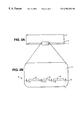
- FIG. 1 illustrates an example of a NPN bipolar transistor.
- the transistor illustrated in FIG. 1 includes a contact 1 .
- the contact 1 may be made of a semiconductor material, such as polycrystalline silicon.
- the contact 1 is formed over a region of a substrate 3 at a location where an emitter 5 of the transistor has been formed.
- a layer 7 of a dielectric material may be arranged on the substrate between the emitter 5 and the contact 1 .
- the dielectric material of the layer 7 is an oxide.
- FIG. 1 also illustrates the doping and flow of current within an NPN bipolar transistor.
- the emitter-base (E-B) junction Under normal bias conditions, or forward active mode, the emitter-base (E-B) junction is forward biased, 5 and 9 in FIG. 1, and the collector base junction, 11 and 9 in FIG. 1 . is reversed biased. Electrons are ejected from the emitter into the base. Then, the electrons diffuse across the base region where they are swept across the reverse biased C-B junction into the collector.
- the collector current I C is associated with the flows of electrons from the emitter.
- the base current I B is a function of the holes ejected from the base region. The holes can either recombine in the single crystal emitter or flow into the polysilicon emitter region 1 , which is usually highly doped polycrystalline silicon.
- Beta may be described by the relationship between the collector current and base current. Beta is defined as (collector current)/(base current). In other words, beta equals I C /I B . Generally, the desired value of beta is 100.
- Resistance created by dielectric material of region 7 may affect the base current, as shown in FIG. 2 .
- base current decreases and, thus, beta increases.
- the resistance of region 7 is low, the resulting base current is high and, thus, beta is low.
- Controlling the dielectric thickness in region 7 for a bipolar transistor typically is critical to controlling the current gain, beta.
- polysilicon polycrystalline
- a horizontal CVD polysilicon deposition tube has been used extensively.
- the polysilicon is deposited on the single crystalline Si emitter after the single crystalline Si has been precleaned.
- dielectric region 7 may be thin since the only oxidation that occurs in region 7 in the transistor illustrated in FIGS. 1 and 2 is that which occurs as the wafers enter the horizontal CVD tube.
- residual oxygen trapped in the system when the wafers are loaded may react with the emitter Si at insert temperatures of approximately 625° C. It has been found that very little oxidation of the emitter Si occurs in this instance.
- the resulting polysilicon is deposited on a Si surface with essentially native oxide.
- Region 7 in this case has a very low resistance and, thus, Beta is low at approximately 50-60. Because the interfacial oxidation is essentially uncontrolled, Beta is found to be highly variable from lot to lot using the horizontal polysilicon deposition process.
- the polysilicon layer over the emitter may be deposited using a vertical chemical vapor deposition (CVD) polysilicon deposition tube in which the Si region of the emitter may be oxidized in situ, typically after an initial wet preclean.
- CVD chemical vapor deposition
- a batch of wafers may be loaded into the furnace, the chamber evacuated and then a mixture of an inert gas and oxygen may be leaked into the chamber at temperatures of approximately 600° C.
- Beta can be set to 100.
- the present invention addresses these and other problems by providing a process for forming at least one interface region between two regions of semiconductor material.
- the process includes forming at least one region of dielectric material comprising nitrogen in the vicinity of at least a portion of a boundary between the two regions of semiconductor material, thereby controlling electrical resistance at the interface.
- the present invention provides semiconductor devices prepared according to the above process.
- the present invention provides a semiconductor device including a region of a first semiconductor material, and a region of a second semiconductor material.
- An interface region including at least one region of at least one dielectric material comprising of nitrogen is arranged in the vicinity of at least a portion of the boundary between the first region of semiconductor material and the second region of semiconductor material thereby controlling electrical resistance at the interface.
- FIG. 1 represents a cross-sectional view of a NPN bipolar transistor
- FIG. 2 represents a combined schematic and cross-sectional view of the embodiment of the transistor illustrated in FIG. 1;
- FIG. 3 a represents a cross-sectional view of a portion of an embodiment of a semiconductor device structure according to the present invention.
- FIG. 3 b represents a close-up cross sectional view of a portion of the embodiment of a semiconductor device according to the present invention as illustrated in FIG. 3 a[.];
- FIG. 4 represents a graph illustrating a relationship between thickness of an oxide layer formed according to an embodiment of a rapid thermal oxidation process according to the present invention with respect to temperature at which the rapid thermal oxidation process is performed;
- FIG. 5 represents a cross-sectional view of an embodiment of a polycrystalline silicon/monocrystalline silicon interface
- FIG. 6 represents a cross-sectional view of another embodiment of a polycrystalline silicon/monocrystalline silicon interface
- FIG. 7 represents across-sectional view of an additional embodiment of a polycrystalline silicon/monocrystalline silicon interface.
- the present invention controls base current, beta, and resistance through at least one region of dielectric material between the polycrystalline silicon emitter and the monocrystalline substrate.
- the dielectric material according to the present invention typically includes nitrogen. As described in greater detail below, the nitrogen may take a variety of forms.
- the present invention is not limited to use at a boundary between monocrystalline and polycrystalline silicon.
- the present invention may be utilized at any interface between two regions of semiconductor material.
- the two regions of semiconductor material could include monocrystalline silicon, polycrystalline silicon, and/or amorphous silicon.
- BiCMOS devices bipolar transistors and FET devices on the same chip.
- the present invention may be utilized with heterojunction and homojunction bipolar transistors, DRAM cells, and any semiconductor device structure that includes amorphous silicon or polycrystalline silicon or SiGe or other materials are deposited on monocrystalline silicon or SiGe.
- the dielectric material between the two regions of a semiconductor material typically includes nitrogen.
- the nitrogen may be in any form.
- the nitrogen could be in the form of implanted N+ or deposited N from a gaseous environment containing N 2 O, NH 3 , and/or NO forming Si x N y (a silicon nitride) and/or Si x O y N z (a silicon oxynitride).
- the thickness of the nitrogen containing dielectric region(s) as well as the percentage of the boundary between the two regions of semiconductor material that the region(s) of dielectric material covers may vary depending upon the embodiment. Typically, the thickness and extent of the dielectric region(s) may depend upon the desired base current, resistance, and/or beta value it is desired that the final structure have.
- the dielectric region(s) may have a thickness of from about 1 ⁇ to about 10 ⁇ .
- the thickness may be measured with an elipsometer.
- the thickness may be in addition to native oxide film also measured with an elipsometer.
- the dielectric material may be film having a thickness of less than one monolayer to a plurality of monolayers. A thickness of less than one monolayer indicates that the film does not entirely cover the boundary between the regions of semiconductor material.
- the dielectric material could also be arranged in a single monolayer that covers the entire boundary between the two regions of semiconductor material.
- Some embodiments may include a plurality of monolayers. According to such an embodiment, regions may exist where no dielectric material is deposited between the regions of semiconductor material while in other regions, a plurality of layers of semiconductor material may be arranged between the regions of semiconductor material. Also according to such embodiments, some regions of the dielectric material may include a plurality layers while other regions include a fewer or greater layers of dielectric material.
- the dielectric material may also include at least one oxide.
- FIG. 3 a illustrates an example of a structure that the present invention may be utilized with.
- FIG. 3 a illustrates a region of monocrystalline silicon 1 , a region of polycrystalline silicon 3 and an interface 5 between the region of monocrystalline silicon and polycrystalline silicon.
- FIG. 3 b illustrates a close-up cross sectional view of a portion of the structure illustrated in FIG. 3 a including a plurality of regions of dielectric material between the two regions of semiconductor material.
- FIG. 3 b illustrates a portion of a structure showing an example of an embodiment of the structure according to the present invention.
- FIG. 3 b illustrates a boundary region 7 including a plurality of regions 9 of dielectric material between the region of monocrystalline silicon 1 and the region of polycrystalline silicon 3 .
- Arrows 12 represent current flowing between the regions of semiconductor material.
- the present invention provides a solution to the above problems by providing a process to control deposition of region 7 in a structure such as the transistor illustrated in FIGS. 1 and 2.
- the processes and resulting structures may also be utilized in other applications. It just happens that the process of the invention is particularly useful in transistors such as those shown in FIGS. 1 and 2.
- the present invention permits control of the value of beta in the resulting structure.
- the present invention accomplishes these and other objects by providing a process for creating a region of the material to form regions 7 in the structure illustrated in FIGS. 1 and 2.
- the present invention provides a rapid thermal oxidation (RTO) process.
- the rapid thermal oxidation process is utilized to form a layer of oxide on the surface of the emitter 5 illustrated in FIGS. 1 and 2.
- the rapid thermal oxidation may be controlled to create oxide on at least of a portion of the emitter. In other words, it is not necessary that the oxide cover the entire emitter area.
- One factor that may control the thickness of the oxide as well as the percentage of the emitter covered by the oxide is the desired value of beta, which as stated above may be affected by the thickness of the oxide layer.
- the rapid thermal oxidation process is carried out at about 500° C.
- the rapid thermal oxidation process may be carried out for about 5 seconds.
- An embodiment of a process according to the present invention included rapid thermal oxidation carried out at about 500° C. for about 5 seconds resulted in formation of an oxide layer having a thickness of about 6A. This oxide thickness includes about 4A of native oxide plus about 2A of oxide formed by the rapid thermal oxidation process.
- the resulting structure has a beta value of about 100. Without this process, the interface oxide was not well controlled and the resulting Beta value was at the low end of the process specification at a value of 60.
- the silicon dioxide or oxide thickness described herein are defined as oxide that is thermally grown plus the native oxide already present on the wafer.
- a monocrystalline Si surface may include 5 ⁇ of native oxide as measured with an ellipsometer commonly used for semiconductor manufacturing. After subjecting this wafer to the rapid thermal oxidation process described herein, the oxide may measure 7A.
- the oxide thickness is defined as a thermally grown oxide of 2A in addition to or plus (+) native oxide of 5 ⁇ .
- the emitter monocrystalline silicon surface may be precleaned with some type of HF chemistry.
- HF chemistry is well know to those of ordinary skill in the art and, therefore, is not discussed further here.
- One of ordinary skill in the art could determine appropriate treatment including HF to utilize without undue experimentation.
- All oxides may be removed from the surface of a monocrystalline silicon substrate such that only native oxide due to exposure of the silicon to the atmosphere remains on the silicon.
- an oxide is grown on the surface of the monocrystalline silicon using a rapid thermal oxidation (RTO) process according to the present invention as described herein.
- the present invention typically results in the growth of about 1 A to about 5 A of thermal oxide.
- This level of thermal oxide is in addition to the native oxide present prior to the RTO process.
- the oxide level may be measured with an ellipsometer commonly used in semiconductor processing. Therefore, if there is approximately 8A of native oxide prior to the RTO process, the measured thickness may be about 9 A to about 13 A post RTO.
- polysilicon may then deposited in a CVD reaction without any additional oxidation of the Si surface.
- FIG. 4 illustrates a relationship between the temperature at which the rapid thermal oxidation is carried out and the resultant thickness of the oxide layer between the emitter and the contact.
- the total oxide as well as the oxide grown by the rapid thermal oxidation process both increase with increasing RTO temperature.
- FIG. 5 shows a situation where polysilicon is deposited on a silicon surface with little oxide other than native oxide between the polysilicon and the monocrystalline silicon.
- the polysilicon seeds on the monocrystalline silicon base and the resulting polysilicon structure may include a significant level of epitaxially grown silicon containing many defects. In this case, the interfacial resistance is low and Beta will thus be low since the structure can result in high base current.
- FIG. 6 depicts the interfacial oxide as a plurality of “islands” of oxide, 19 , separated by regions 17 of epitaxial silicon.
- FIG. 7 illustrates an extreme case, where polysilicon is deposited on a monocrystalline silicon surface with a continuous oxide.
- the resulting film is entirely polysilicon with higher resistance than those described above.
- this structure results in high Beta.
- a rapid thermal oxidation process according to the present invention may be carried out in a rapid thermal processor.
- Rapid thermal processors are devices that can heat substrates rapidly to a target temperature or temperatures, maintain the substrates at the target temperature(s), and cool the substrates rapidly from the target temperature(s). These devices are often used in semiconductor manufacturing where wafers are placed through thermal processes.
- a rapid thermal processor can heat wafers at rates of about 5° C. to about 400° C./sec, with about 30° C./sec being typical.
- These processors can cool wafers at rates of about 5° C. to about 100° C./sec, with about 30° C./sec being typical.
- rapid thermal processors are single wafer processors. In other words, they do not process batches of substrates or wafers simultaneously. Instead, they process one wafer at a time through a prescribed thermal cycle. Because of this, the chamber of a rapid thermal processor typically is small, especially in comparison to the size of the chambers of used in conventional furnace hot processing.
- rapid thermal processing systems typically are closed systems, with control of gas delivery and exhaust. Therefore, during processing, gas concentrations may easily be controlled. For example, oxygen concentration may be controlled during processing at levels of from about 100% pure O2 down to about 10 ppm O2.
- a layer of SiO 2 or other oxide layer may be formed over the monocrystalline semiconductor.
- the oxide layer may be described as a monolayer or less. Less than a monolayer indicates that not all of the surface of the monocrystalline semiconductor is covered with oxide. Less than a monolayer indicates the layer is discontinuous.
- FIG. 3 illustrates the discontinuous layer of the present invention.
- FIG. 3 depicts the oxide layer as comprising a plurality of isolated regions 19 . These isolated regions 19 may be termed “islands.”
- One significant advantage of the present invention is that it can produce a very repeatable oxide layer.
- the coverage and thickness of the oxide on the surface of the monocrystalline semiconductor are very repeatable according to the present invention.
- the thickness of oxide created by the rapid thermal oxidation according to the present invention may vary depending upon the temperature, time, pressure, and/or oxygen concentration at which the rapid thermal oxidation is carried out. Increasing the temperature, time, pressure, or oxygen concentration will have the effect of increasing the thickness of oxide grown. Several different temperature ranges may be included in various embodiments of the present invention. For example, the invention may be carried out at a temperature less than about 700° C.
- Selecting the target temperature of the rapid thermal process at least partially determines the thickness of the oxide layer grown.
- the specific electrical needs of a particular semiconductor device will determine what thickness of oxide is required.
- an extended range of temperatures may be used. Rapid thermal processes within the temperature ranges described herein can result in anywhere from complete coverage of the monocrystalline semiconductor to partial coverage of the monocrystalline semiconductor.
- a device may perform optimally with rapid thermal oxidation at a temperature of about 450° C.
- Another device may require a rapid thermal oxidation at a temperature of about 475° C.
- a typical range for rapid thermal oxidation processing according to the present invention is about 450° C. to about 500° C. However, processing at less than about 450° C. may result-obtaining lower beta values. Processing above about 500° C. may permit higher beta values to be obtained.
- the resulting oxide layer may have a thickness of about 5 ⁇ to about 10 ⁇ .
- the oxide thickness may be no greater than about 5 ⁇ .
- the oxide layer may have a thickness of about 2 ⁇ to about 4 ⁇ or from about 2 ⁇ to about 3 ⁇ when utilizing lower temperature processes.
- the specific thickness of oxide created may be determined by the rapid thermal oxidation process used, including manipulating the variables discussed herein.
- the layer created by the present invention may provide a layer that reduces the tendency of that added semiconductor to deposit or grow epitaxially, or with the monocrystalline pattern of the substrate.
- each wafer or lot of wafers may receive a different rapid thermal oxidation process, if wafer in a batch or lot of wafers may receive a different rapid thermal oxidation process, if desired, allowing wafers to intentionally, and controllably reach a range of performance values.
- the layer between the monocrystalline semiconductor and polycrystalline and/or a amorphous semiconductor may be more broadly described as an electrically insulating material.
- the electric insulating material could be an oxide. However, it could also be a nitride and/or a nitridized oxide.
- the at least one region of dielectric material is arranged on a sidewall of a trench formed in a monocrystalline silicon substrate.
- the trench is filled with non-monocrystalline silicon.
- the trench is filled with polycrystalline silicon or amorphous silicon in which some crystallization has taken place.
- the placement of the region(s) of dielectric material relative to the interface region may depend upon the environment as well as the method utilized for creating the region(s) of dielectric material.
- the atoms or molecules of dielectric material may be implanted within one of the regions of semiconductor material. In other words, the atoms or molecules of dielectric material may be implanted within one or both of the regions of semiconductor material.
- the atoms and/or molecules may be implanted under the surface of one or both of the regions of semiconductor material or at the surface of one or more of the regions of semiconductor material.
- the dielectric material includes nitrogen atoms implanted in the monocrystalline silicon.
- the dielectric material is deposited on a surface of one of the regions of semiconductor material, such as the monocrystalline silicon discussed above.
- the other region of semiconductor material may then be deposited or formed on the monocrystalline substrate and the dielectric region(s).
- the present invention also includes processes for forming at least one interface region between two regions of semiconductor material.
- the method includes forming at least one region of dielectric material including nitrogen in the vicinity of at least a portion of a boundary between two regions of semiconductor material.
- the at least one region of dielectric material may be formed in a variety of ways.
- the at least one region of the dielectric material may be formed by implanting the dielectric material in the vicinity of the surface of one of the regions of semiconductor material.
- the dielectric material may be implanted in one region of dielectric material prior to formation of the other region of semiconductor material.
- the dielectric material is created by implanting low doses of the dielectric material.
- Low doses may be desirable to help ensure that a discontinuous layer of dielectric is formed to result in the desired control of base current.
- low levels of nitrogen are implanted.
- the energy with which the nitrogen or other material(s) is implanted may be low enough such that the material(s) is/are not implanted too deep in the semiconductor material.
- the nitrogen in which low levels of nitrogen are implanted as the dielectric material, the nitrogen is implanted at energies less than about 2 KeV. Typical implant energies may be in a range of about 0.1 KeV to about 5 KeV.
- the dosages of nitrogen utilized in this example may be in a range of from 1 ⁇ 10 11 to 1 ⁇ 10 14 .
- an additional anneal process may be performed.
- the anneal process may be desirable to supplement the implantation process. For example some hot processes may not be adequate to form the discontinuous Si—N layer near the surface of the monocrystalline silicon.
- the anneal process may be a rapid thermal anneal.
- a rapid thermal anneal may be carried out at a temperature of about 900° C. to about 1100° C. for a time of about 1 second to about 60 seconds.
- Such a rapid thermal anneal may be used to form Si x N y (a silicon nitride) and/or Si x N y O z (a silicon oxynitride)
- An advantage of implanting the dielectric material as described above is that photomasks may be utilized for tailoring implant conditions by region or device.
- a blanket film could be implanted in a region of semiconductor material. Residual dielectric may be removed after deposition and etching of the second layer of semiconductor material. For example, nitrogen could be implanted in the monocrystalline silicon as a blanket film. A residual material could be removed postpoly-Si deposition and etch.
- one of the regions of semiconductor material may be subjected to elevated temperatures and a nitrogen-containing gaseous atmosphere.
- the gaseous atmosphere could include at least one N 2 O, NO, and/or NH 3 gases.
- the temperature that the process may be carried out at could be anywhere from about 300° C. to about 1,000° C.
- the semiconductor may be exposed to these temperatures and gases for a time period of about 1 to about 60 seconds.
- the film may include silicon nitride and/or silicon oxynitride.
- the composition of the film may depend upon the nitrogen containing gas utilized in during the process as well as the temperature and time period that the process is carried out for.
- the dielectric material created and the characteristics of the film created may also depend upon the semiconductor material that is exposed to the process of the invention. If the semiconductor material is monocrystalline silicon, then the dielectric material may be silicon nitride or silicon oxynitride if exposed to the above gases at the above process parameters.
- the process may be carried out after cleaning.
- the cleaning may be a wet process, plasma process, or reducing hot process.
- the process for carrying out the formation of the dielectric layer may be a rapid thermal process, fast thermal process (FTP), or conventual furnace process.
- a rapid thermal process typically is a rapid process carried out with quartz lamps.
- a fast thermal process typically is a small batch process that utilizing a conventional furnace.
- a conventional furnace typically utilizes a quartz tube with a ceramic cover and is heated resistively.
- the substrate may be exposed to the elevated temperatures according to a variety of regimens.
- the substrate may be exposed to the full elevated temperature immediately.
- the temperature that the substrate is exposed to may be ramped up over a period of time.
- the temperature that the substrate is exposed to is ramped up at a rate of about 75° C. per second to a temperature of about 400° C. to about 800° C.
- the rate that the temperature may be ramped up may be about 5° per second to about 100° C. per second.
- ammonia gas may flow into the container that the process is being carried out in at a rate of about 5 standard liters per minute (SLPM) for a time of about 5 seconds to about 15 seconds.
- SLPM standard liters per minute
- the substrate After exposing the substrate to elevated temperatures, regardless of whether the temperatures are ramped and the final temperature, the substrate may then be cooled.
- the substrate may be cooled actively or passively.
- the process may include some intervention for increasing the rate of coaling beyond what would be experienced in simple convection of heat from the substrate. to one example, the substrate is cooled at a rate of about 15° C. to about 30° C. per second.
- the substrate may be extracted from a processing chamber or other space where the process is carried out.
- the process according to the second example may result in a dielectric layer having a thickness of about 1 ⁇ to about 10 ⁇ , when measured elipsometrically.
- process parameters may be controlled to produce dielectric layer or layers of any desired thickness and percentage of area coverage of the boundary between the two regions of semiconductor material.
- the second region of semiconductor material may be provided on the first region of semiconductor material and the dielectric region(s).
- the dielectric region(s) may remain through deposition of the second region of semiconductor material. Any residual dielectric material or any dielectric material that is desired to be removed may be removed after or during etch of the second region of semiconductor material.
- a third example of a process according to the present invention may be utilized for forming a dielectric region in the vicinity of a boundary between two regions of semiconductor material includes a very thin chemical vapor deposition process.
- the chemical vapor deposition process may vary from embodiment to embodiment.
- a low pressure chemical vapor deposition process LPCVD
- Another embodiment utilizes a plasma enhanced chemical vapor deposition (PECVD) process.
- PECVD plasma enhanced chemical vapor deposition
- this third example of a process for creating a region(s) of dielectric material may be utilized to create a discontinuous film on one of the regions of semiconductor material.
- the chemical vapor deposition process may be utilized to create a discontinuous film on monocrystalline silicon that may serve as an emitter in a semiconductor device.
- the chemical vapor deposition process may utilize a silicon source gas.
- a silicon source gas that may be utilized with a CVD process according to the third example of the present invention is silane and/or dichlorosilane (DCS).
- Other silicon source gases may also utilized in a chemical vapor deposition process.
- the chemical vapor deposition process may also utilize a nitrogen/oxygen source gas.
- the nitrogen/oxygen source gas may vary, depending upon the embodiment. Examples of nitrogen/oxygen source gases may include NH 3 and N 2 O.
- the ratio of silicon source gas to nitrogen/oxygen source gas may vary to achieve a desired silicon-nitrogen/oxygen stoichiometry.
- the flow and ratio of these gases may also vary depending upon the characteristics of the layer or layers of dielectric material that it is desired to create.
- the ratio of gases in the CVD processes may be controlled to utilize various ratio proportions to produce voids.
- the process parameters of the chemical vapor deposition process utilized may vary depending upon, among other things, the desired characteristics of the dielectric region(s) that is desired to create and the gases that are being utilized.
- the chemical vapor deposition is carried out at a temperature of about 600° C. to about 800° C.
- the gas flow may also vary depending upon the embodiment.
- the deposition gases may flow for a time less than about 5 seconds.
- a chemical vapor deposition process such as described herein may be utilized to create a film of a thickness with less than one monolayer.
- the film may have a thickness of about 1 to about 10 ⁇ .
- the dielectric material may be deposited on a sidewall of trench formed in a monocrystalline silicon substrate, with the trench subsequently being filled with polycrystalline silicon.
- the dielectric region(s) may also include at least one oxide as also described above.
- the present invention also includes a device prepared by a process such as the process described above.
- the present invention may allow tailoring of beta by specific region or device. Additionally, an oxynitride interfacial dielectric may be more robust with subsequent thermal processing in a DRAM structure. Furthermore, a nitride-containing dielectric region may not be consumable by subsequent hot processes.
- the present invention also allows a high degree of control of NPN- ⁇ in polysilicon emitters. A nitrogen containing dielectric region(s) also help reduce retention defects in trench DRAM buried strap processes.
- the present invention may also include a rapid thermal anneal (RTA) when an N implant is utilized to form an Si-N species.
- RTA rapid thermal anneal
Landscapes
- Engineering & Computer Science (AREA)
- Microelectronics & Electronic Packaging (AREA)
- Power Engineering (AREA)
- Physics & Mathematics (AREA)
- Condensed Matter Physics & Semiconductors (AREA)
- General Physics & Mathematics (AREA)
- Computer Hardware Design (AREA)
- Manufacturing & Machinery (AREA)
- Ceramic Engineering (AREA)
- Bipolar Transistors (AREA)
- Formation Of Insulating Films (AREA)
Abstract
Description
Claims (35)
Priority Applications (6)
| Application Number | Priority Date | Filing Date | Title |
|---|---|---|---|
| US09/244,958 US6703283B1 (en) | 1999-02-04 | 1999-02-04 | Discontinuous dielectric interface for bipolar transistors |
| JP2000023868A JP2000228405A (en) | 1999-02-04 | 2000-02-01 | Method of forming interface region between two semiconductor material regions, and semiconductor device |
| KR10-2000-0005422A KR100377714B1 (en) | 1999-02-04 | 2000-02-03 | Discontinuous dielectric interface for bipolar transistors |
| TW089101901A TW498459B (en) | 1999-02-04 | 2000-02-03 | Discontinuous dielectric interface for bipolar transistors |
| US10/653,925 US6939771B2 (en) | 1999-02-04 | 2003-09-04 | Discontinuous dielectric interface for bipolar transistors |
| US11/001,140 US7008852B2 (en) | 1999-02-04 | 2004-12-02 | Discontinuous dielectric interface for bipolar transistors |
Applications Claiming Priority (1)
| Application Number | Priority Date | Filing Date | Title |
|---|---|---|---|
| US09/244,958 US6703283B1 (en) | 1999-02-04 | 1999-02-04 | Discontinuous dielectric interface for bipolar transistors |
Related Child Applications (1)
| Application Number | Title | Priority Date | Filing Date |
|---|---|---|---|
| US10/653,925 Division US6939771B2 (en) | 1999-02-04 | 2003-09-04 | Discontinuous dielectric interface for bipolar transistors |
Publications (1)
| Publication Number | Publication Date |
|---|---|
| US6703283B1 true US6703283B1 (en) | 2004-03-09 |
Family
ID=22924783
Family Applications (3)
| Application Number | Title | Priority Date | Filing Date |
|---|---|---|---|
| US09/244,958 Expired - Lifetime US6703283B1 (en) | 1999-02-04 | 1999-02-04 | Discontinuous dielectric interface for bipolar transistors |
| US10/653,925 Expired - Fee Related US6939771B2 (en) | 1999-02-04 | 2003-09-04 | Discontinuous dielectric interface for bipolar transistors |
| US11/001,140 Expired - Fee Related US7008852B2 (en) | 1999-02-04 | 2004-12-02 | Discontinuous dielectric interface for bipolar transistors |
Family Applications After (2)
| Application Number | Title | Priority Date | Filing Date |
|---|---|---|---|
| US10/653,925 Expired - Fee Related US6939771B2 (en) | 1999-02-04 | 2003-09-04 | Discontinuous dielectric interface for bipolar transistors |
| US11/001,140 Expired - Fee Related US7008852B2 (en) | 1999-02-04 | 2004-12-02 | Discontinuous dielectric interface for bipolar transistors |
Country Status (4)
| Country | Link |
|---|---|
| US (3) | US6703283B1 (en) |
| JP (1) | JP2000228405A (en) |
| KR (1) | KR100377714B1 (en) |
| TW (1) | TW498459B (en) |
Cited By (5)
| Publication number | Priority date | Publication date | Assignee | Title |
|---|---|---|---|---|
| US20040056327A1 (en) * | 1999-02-04 | 2004-03-25 | Ballantine Arne W. | Discontinuous dielectric interface for bipolar transistors |
| US7470594B1 (en) * | 2005-12-14 | 2008-12-30 | National Semiconductor Corporation | System and method for controlling the formation of an interfacial oxide layer in a polysilicon emitter transistor |
| US20110238161A1 (en) * | 2010-03-26 | 2011-09-29 | Battelle Memorial Institute | System and method for enhanced electrostatic deposition and surface coatings |
| US9716136B1 (en) | 2016-03-16 | 2017-07-25 | Globalfoundries Inc. | Embedded polysilicon resistors with crystallization barriers |
| DE102016112877B4 (en) * | 2015-09-07 | 2021-07-15 | Fuji Electric Co., Ltd. | A method of manufacturing a semiconductor device and a semiconductor manufacturing device used for the method |
Citations (31)
| Publication number | Priority date | Publication date | Assignee | Title |
|---|---|---|---|---|
| US3709726A (en) | 1969-01-09 | 1973-01-09 | Ferranti Ltd | Semiconductor devices |
| US3765935A (en) | 1971-08-10 | 1973-10-16 | Bell Telephone Labor Inc | Radiation resistant coatings for semiconductor devices |
| US4363868A (en) | 1979-12-26 | 1982-12-14 | Fujitsu Limited | Process of producing semiconductor devices by forming a silicon oxynitride layer by a plasma CVD technique which is employed in a selective oxidation process |
| JPS59220969A (en) | 1983-05-31 | 1984-12-12 | Matsushita Electric Works Ltd | Manufacture of planar type transistor |
| JPS6417444A (en) | 1987-06-15 | 1989-01-20 | Commissariat Energie Atomique | Manufacture of insulation buried in semiconductor substrate by ion implantation and construction of semiconductor containing the insulation |
| JPH01160051A (en) | 1987-12-17 | 1989-06-22 | Toshiba Corp | Bipolar transistor |
| JPH02265246A (en) | 1989-04-06 | 1990-10-30 | Nec Corp | Bipolar transistor |
| US4992306A (en) | 1990-02-01 | 1991-02-12 | Air Products Abd Chemicals, Inc. | Deposition of silicon dioxide and silicon oxynitride films using azidosilane sources |
| JPH03250737A (en) | 1990-02-28 | 1991-11-08 | Canon Inc | Semiconductor device; electronic apparatus using same semiconductor device |
| JPH0414837A (en) | 1990-05-08 | 1992-01-20 | Fujitsu Ltd | Manufacture of semiconductor device |
| JPH04152533A (en) | 1990-10-16 | 1992-05-26 | Nec Corp | Semiconductor device |
| US5140299A (en) * | 1990-06-19 | 1992-08-18 | At&T Bell Laboratories | Article comprising a high value resistor |
| JPH04321231A (en) | 1991-04-19 | 1992-11-11 | Texas Instr Japan Ltd | Semiconductor device |
| US5194926A (en) * | 1991-10-03 | 1993-03-16 | Motorola Inc. | Semiconductor device having an inverse-T bipolar transistor |
| US5260236A (en) | 1991-06-07 | 1993-11-09 | Intel Corporation | UV transparent oxynitride deposition in single wafer PECVD system |
| US5468974A (en) | 1994-05-26 | 1995-11-21 | Lsi Logic Corporation | Control and modification of dopant distribution and activation in polysilicon |
| US5578856A (en) * | 1993-03-01 | 1996-11-26 | Motorola Inc. | BicMOS device having a bipolar transistor and a MOS triggering transistor |
| JPH08316476A (en) | 1995-05-19 | 1996-11-29 | Sony Corp | Semiconductor device and manufacture thereof |
| US5587344A (en) | 1994-06-03 | 1996-12-24 | Nec Corporation | Method for fabricating an oxynitride film for use in a semiconductor device |
| US5620910A (en) * | 1994-06-23 | 1997-04-15 | Semiconductor Energy Laboratory Co., Ltd. | Method for producing semiconductor device with a gate insulating film consisting of silicon oxynitride |
| US5723368A (en) | 1994-06-23 | 1998-03-03 | Cho; Chi-Chen | Porous dielectric material with improved pore surface properties for electronics applications |
| US5723895A (en) * | 1995-12-14 | 1998-03-03 | Nec Corporation | Field effect transistor formed in semiconductor region surrounded by insulating film |
| JPH1083995A (en) | 1996-09-09 | 1998-03-31 | Sony Corp | Semiconductor device and manufacturing method thereof |
| US5736425A (en) * | 1995-11-16 | 1998-04-07 | Texas Instruments Incorporated | Glycol-based method for forming a thin-film nanoporous dielectric |
| US5744399A (en) | 1995-11-13 | 1998-04-28 | Lsi Logic Corporation | Process for forming low dielectric constant layers using fullerenes |
| US5759904A (en) | 1996-11-06 | 1998-06-02 | Southwest Research Institute | Suppression of transient enhanced diffusion in ion implanted silicon |
| US5763922A (en) | 1997-02-28 | 1998-06-09 | Intel Corporation | CMOS integrated circuit having PMOS and NMOS devices with different gate dielectric layers |
| US5789310A (en) | 1996-12-10 | 1998-08-04 | Advanced Micro Devices, Inc. | Method of forming shallow junctions by entrapment of interstitial atoms |
| US5827769A (en) * | 1996-11-20 | 1998-10-27 | Intel Corporation | Method for fabricating a transistor with increased hot carrier resistance by nitridizing and annealing the sidewall oxide of the gate electrode |
| JPH10335716A (en) | 1997-05-30 | 1998-12-18 | Nec Corp | Manufacturing method of semiconductor device |
| US6228693B1 (en) * | 1998-06-05 | 2001-05-08 | Sharp Laboratories Of America, Inc. | Selected site, metal-induced, continuous crystallization method |
Family Cites Families (6)
| Publication number | Priority date | Publication date | Assignee | Title |
|---|---|---|---|---|
| JPS63289867A (en) | 1987-05-21 | 1988-11-28 | Matsushita Electric Ind Co Ltd | Manufacture of semiconductor device |
| GB2213837B (en) | 1987-12-22 | 1992-03-11 | Philips Electronic Associated | Electronic device manufacture with deposition of material |
| JP3102223B2 (en) | 1993-09-24 | 2000-10-23 | 住友金属工業株式会社 | Oxidation method of silicon substrate |
| JPH0846222A (en) | 1994-05-31 | 1996-02-16 | Texas Instr Inc <Ti> | Injection silicon resonance tunneling diode and its preparation |
| JP3365912B2 (en) | 1996-07-25 | 2003-01-14 | 新日本製鐵株式会社 | Shock wave generator for in-furnace measurement equipment |
| US6703283B1 (en) * | 1999-02-04 | 2004-03-09 | International Business Machines Corporation | Discontinuous dielectric interface for bipolar transistors |
-
1999
- 1999-02-04 US US09/244,958 patent/US6703283B1/en not_active Expired - Lifetime
-
2000
- 2000-02-01 JP JP2000023868A patent/JP2000228405A/en active Pending
- 2000-02-03 KR KR10-2000-0005422A patent/KR100377714B1/en not_active IP Right Cessation
- 2000-02-03 TW TW089101901A patent/TW498459B/en not_active IP Right Cessation
-
2003
- 2003-09-04 US US10/653,925 patent/US6939771B2/en not_active Expired - Fee Related
-
2004
- 2004-12-02 US US11/001,140 patent/US7008852B2/en not_active Expired - Fee Related
Patent Citations (31)
| Publication number | Priority date | Publication date | Assignee | Title |
|---|---|---|---|---|
| US3709726A (en) | 1969-01-09 | 1973-01-09 | Ferranti Ltd | Semiconductor devices |
| US3765935A (en) | 1971-08-10 | 1973-10-16 | Bell Telephone Labor Inc | Radiation resistant coatings for semiconductor devices |
| US4363868A (en) | 1979-12-26 | 1982-12-14 | Fujitsu Limited | Process of producing semiconductor devices by forming a silicon oxynitride layer by a plasma CVD technique which is employed in a selective oxidation process |
| JPS59220969A (en) | 1983-05-31 | 1984-12-12 | Matsushita Electric Works Ltd | Manufacture of planar type transistor |
| JPS6417444A (en) | 1987-06-15 | 1989-01-20 | Commissariat Energie Atomique | Manufacture of insulation buried in semiconductor substrate by ion implantation and construction of semiconductor containing the insulation |
| JPH01160051A (en) | 1987-12-17 | 1989-06-22 | Toshiba Corp | Bipolar transistor |
| JPH02265246A (en) | 1989-04-06 | 1990-10-30 | Nec Corp | Bipolar transistor |
| US4992306A (en) | 1990-02-01 | 1991-02-12 | Air Products Abd Chemicals, Inc. | Deposition of silicon dioxide and silicon oxynitride films using azidosilane sources |
| JPH03250737A (en) | 1990-02-28 | 1991-11-08 | Canon Inc | Semiconductor device; electronic apparatus using same semiconductor device |
| JPH0414837A (en) | 1990-05-08 | 1992-01-20 | Fujitsu Ltd | Manufacture of semiconductor device |
| US5140299A (en) * | 1990-06-19 | 1992-08-18 | At&T Bell Laboratories | Article comprising a high value resistor |
| JPH04152533A (en) | 1990-10-16 | 1992-05-26 | Nec Corp | Semiconductor device |
| JPH04321231A (en) | 1991-04-19 | 1992-11-11 | Texas Instr Japan Ltd | Semiconductor device |
| US5260236A (en) | 1991-06-07 | 1993-11-09 | Intel Corporation | UV transparent oxynitride deposition in single wafer PECVD system |
| US5194926A (en) * | 1991-10-03 | 1993-03-16 | Motorola Inc. | Semiconductor device having an inverse-T bipolar transistor |
| US5578856A (en) * | 1993-03-01 | 1996-11-26 | Motorola Inc. | BicMOS device having a bipolar transistor and a MOS triggering transistor |
| US5468974A (en) | 1994-05-26 | 1995-11-21 | Lsi Logic Corporation | Control and modification of dopant distribution and activation in polysilicon |
| US5587344A (en) | 1994-06-03 | 1996-12-24 | Nec Corporation | Method for fabricating an oxynitride film for use in a semiconductor device |
| US5620910A (en) * | 1994-06-23 | 1997-04-15 | Semiconductor Energy Laboratory Co., Ltd. | Method for producing semiconductor device with a gate insulating film consisting of silicon oxynitride |
| US5723368A (en) | 1994-06-23 | 1998-03-03 | Cho; Chi-Chen | Porous dielectric material with improved pore surface properties for electronics applications |
| JPH08316476A (en) | 1995-05-19 | 1996-11-29 | Sony Corp | Semiconductor device and manufacture thereof |
| US5744399A (en) | 1995-11-13 | 1998-04-28 | Lsi Logic Corporation | Process for forming low dielectric constant layers using fullerenes |
| US5736425A (en) * | 1995-11-16 | 1998-04-07 | Texas Instruments Incorporated | Glycol-based method for forming a thin-film nanoporous dielectric |
| US5723895A (en) * | 1995-12-14 | 1998-03-03 | Nec Corporation | Field effect transistor formed in semiconductor region surrounded by insulating film |
| JPH1083995A (en) | 1996-09-09 | 1998-03-31 | Sony Corp | Semiconductor device and manufacturing method thereof |
| US5759904A (en) | 1996-11-06 | 1998-06-02 | Southwest Research Institute | Suppression of transient enhanced diffusion in ion implanted silicon |
| US5827769A (en) * | 1996-11-20 | 1998-10-27 | Intel Corporation | Method for fabricating a transistor with increased hot carrier resistance by nitridizing and annealing the sidewall oxide of the gate electrode |
| US5789310A (en) | 1996-12-10 | 1998-08-04 | Advanced Micro Devices, Inc. | Method of forming shallow junctions by entrapment of interstitial atoms |
| US5763922A (en) | 1997-02-28 | 1998-06-09 | Intel Corporation | CMOS integrated circuit having PMOS and NMOS devices with different gate dielectric layers |
| JPH10335716A (en) | 1997-05-30 | 1998-12-18 | Nec Corp | Manufacturing method of semiconductor device |
| US6228693B1 (en) * | 1998-06-05 | 2001-05-08 | Sharp Laboratories Of America, Inc. | Selected site, metal-induced, continuous crystallization method |
Non-Patent Citations (1)
| Title |
|---|
| U.S. patent application Ser. No. 09/165,946, filed Oct. 2, 1998. |
Cited By (8)
| Publication number | Priority date | Publication date | Assignee | Title |
|---|---|---|---|---|
| US20040056327A1 (en) * | 1999-02-04 | 2004-03-25 | Ballantine Arne W. | Discontinuous dielectric interface for bipolar transistors |
| US20050093053A1 (en) * | 1999-02-04 | 2005-05-05 | Ballantine Arne W. | Discontinuous dielectric interface for bipolar transistors |
| US6939771B2 (en) * | 1999-02-04 | 2005-09-06 | International Business Machines Corporation | Discontinuous dielectric interface for bipolar transistors |
| US7008852B2 (en) * | 1999-02-04 | 2006-03-07 | International Business Machines Corporation | Discontinuous dielectric interface for bipolar transistors |
| US7470594B1 (en) * | 2005-12-14 | 2008-12-30 | National Semiconductor Corporation | System and method for controlling the formation of an interfacial oxide layer in a polysilicon emitter transistor |
| US20110238161A1 (en) * | 2010-03-26 | 2011-09-29 | Battelle Memorial Institute | System and method for enhanced electrostatic deposition and surface coatings |
| DE102016112877B4 (en) * | 2015-09-07 | 2021-07-15 | Fuji Electric Co., Ltd. | A method of manufacturing a semiconductor device and a semiconductor manufacturing device used for the method |
| US9716136B1 (en) | 2016-03-16 | 2017-07-25 | Globalfoundries Inc. | Embedded polysilicon resistors with crystallization barriers |
Also Published As
| Publication number | Publication date |
|---|---|
| TW498459B (en) | 2002-08-11 |
| US7008852B2 (en) | 2006-03-07 |
| KR20000057919A (en) | 2000-09-25 |
| US6939771B2 (en) | 2005-09-06 |
| US20050093053A1 (en) | 2005-05-05 |
| JP2000228405A (en) | 2000-08-15 |
| KR100377714B1 (en) | 2003-03-26 |
| US20040056327A1 (en) | 2004-03-25 |
Similar Documents
| Publication | Publication Date | Title |
|---|---|---|
| EP0090940B1 (en) | Method of forming emitter and intrinsic base regions of a bipolar transistor | |
| US5194397A (en) | Method for controlling interfacial oxide at a polycrystalline/monocrystalline silicon interface | |
| US6794713B2 (en) | Semiconductor device and method of manufacturing the same including a dual layer raised source and drain | |
| JP4340830B2 (en) | Method for forming gate insulating film of semiconductor device | |
| US6197701B1 (en) | Lightly nitridation surface for preparing thin-gate oxides | |
| KR100642627B1 (en) | Method for producing a polycrystalline silicon structure | |
| JP2839018B2 (en) | Method for manufacturing semiconductor device | |
| US20020003286A1 (en) | Vertical bipolar transistor including an extrinsic base with reduced roughness, and fabrication process | |
| JPH05102298A (en) | Trench filling method and method for forming contact points of plurality of sublayers | |
| US20030207530A1 (en) | Shallow trench isolation process for reduced junction leakage | |
| US5242859A (en) | Highly doped semiconductor material and method of fabrication thereof | |
| US5256162A (en) | Apparatus for forming shallow electrical junctions | |
| US6703283B1 (en) | Discontinuous dielectric interface for bipolar transistors | |
| US6451660B1 (en) | Method of forming bipolar transistors comprising a native oxide layer formed on a substrate by rinsing the substrate in ozonated water | |
| US7439607B2 (en) | Beta control using a rapid thermal oxidation | |
| EP0813232B1 (en) | Method of reducing the amount of carbon in an interface between an epitaxial film and a Si substrate | |
| JP2002543608A (en) | Method of forming defects in lattice structure of semiconductor material | |
| US20020081811A1 (en) | Low-temperature deposition of silicon nitride/oxide stack | |
| EP1217652B1 (en) | A method for controlling interfacial oxide at a polycrystalline/monocrystalline silicon interface | |
| Hsieh et al. | Shallow junction formation by dopant diffusion from in situ doped polycrystalline silicon chemically vapor deposited in a rapid thermal processor | |
| KR100469221B1 (en) | A process for device fabrication in which a thin layer of cobalt silicide is formed | |
| Snnikrishnan et al. | Applications of rapid thermal chemical vapor deposition technology to ULSI material processing and device fabrication | |
| Yoon et al. | Recent developments in RT-CVD technology for ULSI material processing and device fabrication: an overview | |
| KR20020010629A (en) | Method for generating defects in a grid support of a semiconductor material |
Legal Events
| Date | Code | Title | Description |
|---|---|---|---|
| AS | Assignment |
Owner name: INTERNATIONAL BUSINESS MACHINES CORPORATION, NEW Y Free format text: ASSIGNMENT OF ASSIGNORS INTEREST;ASSIGNORS:BALLANTINE, ARNE W.;COOLBAUGH, DOUGLAS D.;GILBERT, JEFFREY;AND OTHERS;REEL/FRAME:009772/0399 Effective date: 19990204 |
|
| FEPP | Fee payment procedure |
Free format text: PAYOR NUMBER ASSIGNED (ORIGINAL EVENT CODE: ASPN); ENTITY STATUS OF PATENT OWNER: LARGE ENTITY |
|
| STCF | Information on status: patent grant |
Free format text: PATENTED CASE |
|
| FPAY | Fee payment |
Year of fee payment: 4 |
|
| FPAY | Fee payment |
Year of fee payment: 8 |
|
| FPAY | Fee payment |
Year of fee payment: 12 |
|
| AS | Assignment |
Owner name: GLOBALFOUNDRIES U.S. 2 LLC, NEW YORK Free format text: ASSIGNMENT OF ASSIGNORS INTEREST;ASSIGNOR:INTERNATIONAL BUSINESS MACHINES CORPORATION;REEL/FRAME:036550/0001 Effective date: 20150629 |
|
| AS | Assignment |
Owner name: GLOBALFOUNDRIES INC., CAYMAN ISLANDS Free format text: ASSIGNMENT OF ASSIGNORS INTEREST;ASSIGNORS:GLOBALFOUNDRIES U.S. 2 LLC;GLOBALFOUNDRIES U.S. INC.;REEL/FRAME:036779/0001 Effective date: 20150910 |
|
| AS | Assignment |
Owner name: WILMINGTON TRUST, NATIONAL ASSOCIATION, DELAWARE Free format text: SECURITY AGREEMENT;ASSIGNOR:GLOBALFOUNDRIES INC.;REEL/FRAME:049490/0001 Effective date: 20181127 |
|
| AS | Assignment |
Owner name: GLOBALFOUNDRIES INC., CAYMAN ISLANDS Free format text: RELEASE BY SECURED PARTY;ASSIGNOR:WILMINGTON TRUST, NATIONAL ASSOCIATION;REEL/FRAME:054636/0001 Effective date: 20201117 |
|
| AS | Assignment |
Owner name: GLOBALFOUNDRIES U.S. INC., NEW YORK Free format text: RELEASE BY SECURED PARTY;ASSIGNOR:WILMINGTON TRUST, NATIONAL ASSOCIATION;REEL/FRAME:056987/0001 Effective date: 20201117 |