EP0809114A1 - Drehstoppmessaufnehmer - Google Patents
Drehstoppmessaufnehmer Download PDFInfo
- Publication number
- EP0809114A1 EP0809114A1 EP96939330A EP96939330A EP0809114A1 EP 0809114 A1 EP0809114 A1 EP 0809114A1 EP 96939330 A EP96939330 A EP 96939330A EP 96939330 A EP96939330 A EP 96939330A EP 0809114 A1 EP0809114 A1 EP 0809114A1
- Authority
- EP
- European Patent Office
- Prior art keywords
- light
- circuit
- output
- signal
- rotation
- Prior art date
- Legal status (The legal status is an assumption and is not a legal conclusion. Google has not performed a legal analysis and makes no representation as to the accuracy of the status listed.)
- Withdrawn
Links
Images




Classifications
-
- G—PHYSICS
- G01—MEASURING; TESTING
- G01P—MEASURING LINEAR OR ANGULAR SPEED, ACCELERATION, DECELERATION, OR SHOCK; INDICATING PRESENCE, ABSENCE, OR DIRECTION, OF MOVEMENT
- G01P3/00—Measuring linear or angular speed; Measuring differences of linear or angular speeds
- G01P3/42—Devices characterised by the use of electric or magnetic means
- G01P3/44—Devices characterised by the use of electric or magnetic means for measuring angular speed
- G01P3/48—Devices characterised by the use of electric or magnetic means for measuring angular speed by measuring frequency of generated current or voltage
- G01P3/481—Devices characterised by the use of electric or magnetic means for measuring angular speed by measuring frequency of generated current or voltage of pulse signals
- G01P3/486—Devices characterised by the use of electric or magnetic means for measuring angular speed by measuring frequency of generated current or voltage of pulse signals delivered by photo-electric detectors
-
- G—PHYSICS
- G01—MEASURING; TESTING
- G01D—MEASURING NOT SPECIALLY ADAPTED FOR A SPECIFIC VARIABLE; ARRANGEMENTS FOR MEASURING TWO OR MORE VARIABLES NOT COVERED IN A SINGLE OTHER SUBCLASS; TARIFF METERING APPARATUS; MEASURING OR TESTING NOT OTHERWISE PROVIDED FOR
- G01D5/00—Mechanical means for transferring the output of a sensing member; Means for converting the output of a sensing member to another variable where the form or nature of the sensing member does not constrain the means for converting; Transducers not specially adapted for a specific variable
- G01D5/12—Mechanical means for transferring the output of a sensing member; Means for converting the output of a sensing member to another variable where the form or nature of the sensing member does not constrain the means for converting; Transducers not specially adapted for a specific variable using electric or magnetic means
- G01D5/244—Mechanical means for transferring the output of a sensing member; Means for converting the output of a sensing member to another variable where the form or nature of the sensing member does not constrain the means for converting; Transducers not specially adapted for a specific variable using electric or magnetic means influencing characteristics of pulses or pulse trains; generating pulses or pulse trains
-
- G—PHYSICS
- G01—MEASURING; TESTING
- G01P—MEASURING LINEAR OR ANGULAR SPEED, ACCELERATION, DECELERATION, OR SHOCK; INDICATING PRESENCE, ABSENCE, OR DIRECTION, OF MOVEMENT
- G01P13/00—Indicating or recording presence, absence, or direction, of movement
-
- G—PHYSICS
- G01—MEASURING; TESTING
- G01P—MEASURING LINEAR OR ANGULAR SPEED, ACCELERATION, DECELERATION, OR SHOCK; INDICATING PRESENCE, ABSENCE, OR DIRECTION, OF MOVEMENT
- G01P21/00—Testing or calibrating of apparatus or devices covered by the preceding groups
- G01P21/02—Testing or calibrating of apparatus or devices covered by the preceding groups of speedometers
Definitions
- the present invention relates to a rotation stopped detection sensor for detecting a rotation stopped condition of a rotation body, and in particular to sensor technology for detecting such a rotation stopped condition of a rotation body using a light beam.
- the rotation stopped detection sensor comprises; a single optical sensor and a rotation disk (referred to hereunder simply as a disk) with an outer peripheral portion thereof having approximately equal width transparent portions which pass a light beam and opaque portions which do not pass a light beam.
- the optical sensor has a light source which generates an AC light beam by means of an AC signal from a signal generator, and a light receiving element for receiving the light beam from the light source, positioned facing each other on opposite sides of the outer peripheral portion of the disk, and generates from an output circuit, an output signal corresponding to a light received output from the light receiving element.
- the transparent portions and the opaque portions alternately intersect the light beam. Since the widths of the transparent portions and the opaque portions are approximately the same, then the output from the light receiving element of the optical sensor has an output form with a high level condition and a low level condition appearing alternately at approximately even interval following to the passing of the transparent portions and the opaque portions with rotation of the disk. Since the light source is driven by an AC signal from the signal generator, then in the case where the signal frequency of the signal generator is substantially higher than the rotational speed of the disk, the output signal from the optical sensor in the high level interval where the light beam is received, becomes an AC signal which is switched at the signal frequency of the signal generator.
- the output condition of the optical sensor is fixed at either a high level condition or a low level condition.
- the case can be considered where, when rotation of the disk is stopped, an indicator lamp is illuminated, for example for advising personnel that the vicinity of the disk is "not dangerous".
- an indicator lamp In order to illuminate the indicator lamp with an output signal from the optical sensor, if when the disk is stopped, a light beam is passed so that the output signal from the optical sensor becomes a high level condition, the indicator lamp can be illuminated directly by the output energy from the optical sensor.
- the disk will not always stop at a position where the light beam is passed. In the case where the disk stops at a position where the light beam is shut off, then the indicator lamp cannot be illuminated directly by the output signal from the optical sensor.
- the circuit configuration is such that a light received output from an optical sensor is rectified by a rectifying circuit, and a rectified output therefrom is then input to an on-delay circuit via a NOT circuit. An indicator lamp is then illuminated by an output from the on-delay circuit.
- the rectifying circuit in this case is a device for rectifying the envelope of the AC output signal from the optical sensor which is based on the passing and shut off of the light beam due to rotation of the disk. It has no rectifying function with respect to the AC signal having the frequency of the signal generator. That is to say, the envelope of the AC output signal from the optical sensor due to the passing of the transparent and opaque portions of the rotation disk is treated as the AC signal, and this AC signal is rectified by the rectifying circuit.
- the output condition from the optical sensor is fixed and hence does not become alternating. Consequently, since if the disk is stopped, the rectified output from the rectifying circuit is always at a zero level, and the output signal from the NOT circuit is thus always a high level, then the indicator lamp can be illuminated after a predetermined time lapse by the output from the on-delay circuit.
- the same can also occur in the case where the light source malfunctions so that light is not produced, or the light receiving element malfunctions so that light cannot be converted to an electrical signal, or the light source or light receiving element attachment becomes disconnected (in the case where the light receiving element is provided independent of the output circuit).
- the present invention takes into consideration the above situations with the object of providing a rotation stopped detection sensor which can advise of a rotation body stopped condition by for example illumination of an indicator lamp, without using a NOT circuit to carry out a NOT operation on the output signal from the optical sensor.
- the rotation stopped detection sensor has a plurality of optical sensors each incorporating a light emitting device and a light receiving device, and a rotation body with an optical guide portion for guiding light from the light emitting devices to the light receiving devices, and a light shut off portion for shutting off light from the light emitting devices which is incident on the light receiving devices, disposed alternately thereon in a circumferential direction, the optical sensors being disposed such that when the rotation body is in a stopped condition, at least one or more of the plurality of optical sensors is at a position where light is received via an optical guide portion of said rotation body.
- the arrangement may be such that the rotation body comprises transparent portions and opaque portions disposed alternately in the circumferential direction, and the plurality of optical sensors are constructed such that the light emitting device and the light receiving device are disposed on either side of the rotation body and facing each other.
- the arrangement may be such that the rotation body is constructed with light reflecting portions and non reflecting portions disposed alternately in the circumferential direction, and the plurality of optical sensors are constructed such that the light emitting device and the light receiving device are disposed on the same side with respect to the rotation body.
- the arrangement may be such that the respective optical sensors are constructed such that an AC light beam is produced from the light emitting device due to an AC signal from a signal generator, and this light beam is received by the light receiving device and an AC output signal is produced, and there are provided for each of the optical sensors, a rectifying circuit for rectifying the AC output signal from the optical sensor, and an on-delay circuit for generating a delay output signal after lapse of a predetermined time from input thereto of a rectified output signal from the rectifying circuit, and in addition there is provided a logical sum circuit for carrying out a logical sum operation on the delay outputs from the respective on-delay circuits, the construction being such that when an output from the logical sum circuit is a logic value 1, the rotation body is in a stopped condition.
- an AC signal with a pulse width corresponding to the rotational speed of the rotation body is generated from the respective optical sensors. If the pulse width of this AC signal is shorter than the delay time of the on-delay circuit, then the output from the on-delay circuit becomes a low level advising that the rotation body is rotating, while when this becomes longer than the delay time of the on-delay circuit, the output from the on-delay circuit becomes a high level advising that rotation has stopped. That is to say, the high level condition output indicating the stopped condition of the rotation body, is produced only when the rotation body is stopped and the output from the optical sensor is maintained at a high level for longer than a predetermined time. Furthermore, if a fault occurs for example in the optical sensor, the output becomes a low level and hence fail safe characteristics are improved.
- each of the respective optical sensors When the construction of each of the respective optical sensors is such that a DC signal is applied to the light emitting device to produce a light beam, and this light beam is received by the light receiving device and a DC output signal is produced, then arrangement may be such that there is provided a checking signal generator for applying a checking signal to the light emitting device in order to intermittently stop the light beam emitting operation of the light emitting device, and a NOT circuit for carrying out a NOT operation on the checking signal from the checking signal generator, and in addition there is provided for each respective optical sensor, a first logical sum circuit into which is respectively input via an AC coupling device, an output signal from the optical sensor and an output signal from the NOT circuit, for carrying out a logical sum operation, and an on-delay circuit for generating a delay output signal after lapse of a predetermined time from input thereto of a logical output signal from the first logical sum circuit, and there is provided a second logical sum circuit for carrying out a logical sum operation on the delay outputs from the respective on
- the construction is as above, then also when an optical sensor is driven using a DC signal, it is possible to have a low level output condition at the time of a fault. Hence the fail-safe characteristics can be ensured. Moreover, due to the checking signal from the checking signal generator, the construction has a checking function for checking the normalcy of the output conditions from the optical sensor.
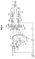
- FIG. 1 is a circuit diagram illustrating a first embodiment of a rotation stopped detection sensor according to the present invention.
- a rotation disk 22 (referred to hereunder simply as a disk 22) serving as a rotation body which is axially supported on a rotation shaft 21, is provided on an outer peripheral portion thereof with transparent portions X 1 , X 2 , X 3 , X 4 serving as optical guide portions which pass light beams PB1, PB2, and opaque portions Y 1 , Y 2 , Y 3 , Y 4 serving as light shut off portions which do not pass light, having approximately equal width around the circumferential direction.
- a plurality (in this case two) optical sensors 23A, 23B incorporate light sources 24A, 24B serving as respective light emitting devices, light receiving elements 25A, 25B serving as respective light receiving devices, and output circuits 26A, 26B respectively connected to the respective light receiving elements 25A, 25B.
- the respective light sources 24A, 24B are respectively connected to a signal generator 27 which generates an AC signal of frequency f1.
- the light sources 24A, 24B and the light receiving elements 25A, 25B are positioned facing each other on opposite sides of the disk 22, and when the disk 22 is stopped, one or other of the optical sensors 23A, 23B is opposite the location of one of the transparent portions X 1 , X 2 , X 3 , X 4 of the disk 22.
- Outputs a, a' from the output circuits 26A, 26B are rectified by respective rectifying circuits 28A, 28B.
- a rectified output b from the rectifying circuit 28A is input to an on-delay circuit 29A, while a rectified output b' from the rectifying circuit 28B is input to an on-delay circuit 29B.
- the rectifying circuits 28A, 28B have the function of rectifying the output signal of frequency f1 from the signal generator 27.
- Respective delay outputs c, c' from the on-delay circuits 29A, 29B are input to an OR circuit 30 serving as a logical sum circuit, and a logical output d from the OR circuit 30 is then used for controlling the illumination or extinguishing of an indicator lamp 31.
- the rectifying circuits 28A, 28B are heretofore known voltage doubler rectifying circuits such as disclosed in U.S. Pat. No. 5,345,138. These voltage doubler rectifying circuits, as shown in FIG. 2, comprise two capacitors C 1 , C 2 and two diodes D 1 , D 2 , configured such that an output signal is output clamped at a constant voltage Vcc.
- the on-delay circuits 29A, 29B are heretofore known devices such as disclosed in WO94/23303, comprising a PUT oscillation circuit and a self hold circuit which uses a fail-safe window comparator/AND gate. These have a fail-safe construction in that only when an input signal equal to or greater than a predetermined level is applied, and the PUT oscillation circuit is operating normally producing an oscillating output, is a high level delay output generated, while at the time of a fault, an output is not produced.
- the transparent portions X 1 , X 2 , X 3 , X 4 of the disk 22 intersect one or other of the light beams PB1 and PB2 of the respective optical sensors 23A and 23B. Consequently, during rotation of the disk 22, the outputs a, a' of the output circuits 26A, 26B of the optical sensors 23A, 23B, as shown by the time chart of FIG. 3, switch alternately on and off (received/shut off). Furthermore, the respective outputs a, a' during the ON period in FIG. 3 become AC signals of frequency f1.
- the two rectifying circuits 28A, 28B respectively rectify the AC signals of frequency f1 which are produced alternately from the output circuits 26A, 26B based on the output frequency of the signal generator 27.
- envelope detection of an AC signal of frequency f1 is carried out by the rectifying circuits 28A, 28B.
- Rectified outputs b, b' with alternate high levels as shown in the time chart of FIG. 3 are thus generated alternately from the rectifying circuits 28A, 28B.
- the output b' on the rectifying circuit 28B side is maintained at a high level condition.
- the on-delay circuits 29A, 29B generate an output voltage signal when the output signals from the rectifying circuits 28A, 28B continue at a high level condition for longer than a predetermined time T ON . Consequently, in this case at the point in time when the high level condition of the rectified output b' on the rectifying circuit 28B side, continues for the predetermined time T ON , the output c' from the on-delay circuit 29B becomes a high level.
- the logical output d from the OR circuit 30 becomes a logic value 1 (high level) and the indicator lamp 31 comes on advising that the disk 22 has stopped.
- the stopping of the disk 22 can be advised by illumination of the indicator lamp 31, without including a NOT circuit (without carrying out a NOT operation).
- both of the light sources 24A, 24B have a fault so that the light beams PB1, PB2 are not produced, or if both of the light receiving elements 25A, 25B have a disconnection fault, then the outputs a, a' from the output circuits 26A, 26B both become a low level and hence the indicator lamp 31 does not come on. Furthermore, if the light receiving elements 25A, 25B have a short circuit fault, then the outputs from the output circuits 26A, 26B do not change, remaining at a constant value. Therefore outputs from the rectifying circuits 28A, 28B are not produced (outputs b, b' are a low level) and hence the indicator lamp 31 does not come on.
- the rectifying circuits 28A, 28B and the on-delay circuits 29A, 29B have a fail safe construction such that an output is not produced at the time of a fault, then also if a fault occurs in these circuits, the indicator lamp 31 will not come on.
- the rotation stopped detection sensor of this embodiment has a fail safe construction in that at the time of a sensor fault, the indicator lamp 31 will not come on.
- the rotation stopped detection sensor of this embodiment is configured as a dual system which uses only one indicator lamp (i.e. the indicator lamp on the side including the NOT operation of the conventional circuit which is not used).
- the construction is such that an AC signal is applied to the light sources 24A, 24B to give illumination, however a DC signal may instead be used.
- the rectifying circuits 28A, 28B can be omitted.
- a DC signal is used, then if a short circuit fault occurs for example in the light receiving elements 25A, 25B, there is the possibility of a high level output being generated from the on-delay circuits 29A, 29B.
- FIG. 4 illustrates a second embodiment of the present invention having a fail-safe construction using a DC signal.
- Components the same as those of the first embodiment illustrated in FIG. 1 are denoted by the same symbol and description is omitted.
- a DC signal Vcc is applied to light sources 24A, 24B.
- a checking signal generator 41 Also applied to the light sources 24A, 24B from a checking signal generator 41 is a light extinguishing pulse signal serving as a checking signal, and having a pulse width of a time t sufficiently shorter than a receiving time in which the light receiving elements 25A, 25B are receiving light beams PB1, PB2 when the disk 22 is rotating.
- An output e from the checking signal generator 41 is input to a NOT circuit 42, and an output e' from the NOT circuit 42 is respectively input to OR circuits 43A, 43B serving as first logical sum circuits into which is respectively input outputs a, a' from optical sensors 23A, 23B.
- Logical outputs b, b' from the respective OR circuits 43A, 43B are input to on-delay circuits 29A, 29B having the same construction as with the first embodiment.
- Outputs c, c' from the on-delay circuits 29A, 29B are input to an OR circuit 30 serving as a second logical sum circuit the same as with the first embodiment, and an indicator lamp 31 is then controlled by an output d from the OR circuit 30.
- the OR circuits 43A, 43B serving as first logical sum circuits, are constructed as shown in FIG. 5. Since these both have the same construction, only that of the OR circuit 43A is given in FIG. 5.
- This comprises two coupling capacitors C 3 , C 4 , two clamping diodes D 3 , D 5 for clamping the input signals which are respectively transmitted via the coupling capacitors C 3 , C 4 , at a constant voltage Vcc, and two rectifying diodes D 4 , D 6 .
- the construction is such that an output a from the optical sensors 23A and an output e' from the NOT circuit 42 are input via the coupling capacitors C 3 , C 4 which serve as respective AC coupling devices, and output terminals of the rectifying diodes D 4 , D 6 are connected to give a wired OR circuit.
- the outputs a, a' from the optical sensors 23A, 23B become alternate high levels following the rotation of the disk 22.
- a pulse signal (a signal of pulse width t) is generated from the checking signal generator 41, while a transparent portion X 1 , X 2 , X 3 or X 4 is intersecting a light beam PB1 or PB2, then as shown by the time chart of FIG. 6, the output a, or a' of the respective optical sensors 23A, 23B becomes a low level.
- the OR circuits 43A, 43B then generate logical sum outputs b, b' for the outputs a, a' from the optical sensors 23A, 23B and the NOT output e' from the NOT circuit 42 which is based on the pulse signal e. While the disk 22 is rotating, the periods of the high level conditions for the logical sum outputs b, b' from the OR circuits 43A, 43B, are shorter than the delay times T ON of the on-delay circuits 29A, 29B. Therefore the outputs c, c' from the on-delay circuits 29A, 29B both become a low level and the indicator lamp 31 is not illuminated.
- the output a' from the optical sensor 23B is maintained at a high level.
- the light source 24B is extinguished by the pulse signal of pulse width t from the checking signal generator 41, this output a' becomes a low level, and at this time, the NOT output e' from the NOT circuit 42 becomes a high level.
- the output a' from the optical sensor 23B is synchronized with the generation of the pulse signal (a signal of pulse width t) serving as the checking signal, and thus intermittently becomes a low level.
- the NOT output e' from the NOT circuit 42 also is synchronized with the generation of the pulse signal, becoming a high level. Both outputs a' and e' are then input to the OR circuit 43B. Consequently, when the disk 22 stops in the condition of FIG. 4, the logical output b' from the OR circuit 43B is maintained at a high level condition corresponding to logic value 1, and if this continues for longer than the delay time T ON of the on-delay circuit 29B, then the output c' from the on-delay circuit 29B becomes a high level and the indicator lamp 31 comes on thus advising that the disk 22 has stopped.
- the logical output b from the OR circuit 43A is also synchronized with the pulse signal (the signal of pulse width t) from the checking signal generator 41, becoming a high level. However, since this is for a sufficiently shorter time than the delay time T ON of the on-delay circuit 29A (t ⁇ T ON ), then the output c from the on-delay circuit 29A remains at a low level condition.
- the outputs b, b' from the OR circuits 43A, 43B become intermittent high levels synchronized with the outputs a, a' from the optical sensors 23A, 23B.
- the delay time T ON of the on-delay circuits 29A, 29B is set longer than the generation interval T (T ON > T) of the pulse signal (the signal of pulse width t)
- the outputs c, c' from the on-delay circuits 29A, 29B will remain at a low level and the indicator lamp 31 will thus become extinguished indicating that the disk 22 is rotating (danger).
- the construction is such that the light beams from the light sources pass through the disk and are received by the light receiving elements.
- the light beams in the first and second embodiments can instead be reflected by the disk and the reflected beams then received by the light receiving elements.
- FIG. 7 shows a construction for the case where the light beams are reflected. Components the same as in the beforementioned embodiments are indicated by the same symbols and description is omitted.
- a disk 22' axially supported on a rotation shaft 21' has instead of the transparent portions X 1 , X 2 , X 3 , X 4 and the opaque portions Y 1 , Y 2 , Y3, Y4 of the first and second embodiments, reflection portions X 1 ', X 2 ', X 3 ', X 4 ' serving as optical guide portions for reflecting light beams PB1, PB2, and non reflection portions Y 1 ', Y 2 ', Y 3 ', Y 4 ' serving as light shut off portions which do not reflect the light beams PB1, PB2, each having approximately equal width around the circumferential direction of an outer peripheral portion of the disk 22'.
- Respective optical sensors 23A, 23B are constructed with respective light sources 24A, 24B and light receiving elements 25A, 25B located on the same side of the disk 22' so that the light receiving element 25A receives the reflected light of the light beam from the light source 24A, and the light receiving element 25B receives the reflected light of the light beam from the light source 24B. Moreover, the optical sensors 23A, 23B are located such that when the disk 22' is stopped, one or other receives reflected light from one of the reflecting portions X 1 ', X 2 ', X 3 ', X 4 ' . Respective outputs a, a' from respective output circuits 26A, 26B are processed using the same circuit configuration as shown in FIG. 1. Furthermore, in the case where instead of the signal generating circuit 27, a DC signal Vcc is used, then the respective outputs a, a' can be processed using the same circuit configuration as shown in FIG. 4.
- the construction has been for two optical sensors and two light beams, however obviously three or more optical sensors can be used.
- the number of inputs to the respective OR circuits corresponding to first logical sum circuits can be increased to correspond to the number of optical sensors.
Landscapes
- Physics & Mathematics (AREA)
- General Physics & Mathematics (AREA)
- Optical Transform (AREA)
- Indicating Or Recording The Presence, Absence, Or Direction Of Movement (AREA)
Applications Claiming Priority (5)
| Application Number | Priority Date | Filing Date | Title |
|---|---|---|---|
| JP322060/95 | 1995-12-11 | ||
| JP32206095 | 1995-12-11 | ||
| JP334510/95 | 1995-12-22 | ||
| JP7334510A JPH09222435A (ja) | 1995-12-11 | 1995-12-22 | 回転停止センサ |
| PCT/JP1996/003511 WO1997022008A1 (fr) | 1995-12-11 | 1996-11-29 | Capteur d'arret de rotation |
Publications (2)
| Publication Number | Publication Date |
|---|---|
| EP0809114A1 true EP0809114A1 (de) | 1997-11-26 |
| EP0809114A4 EP0809114A4 (de) | 1999-03-10 |
Family
ID=26570674
Family Applications (1)
| Application Number | Title | Priority Date | Filing Date |
|---|---|---|---|
| EP96939330A Withdrawn EP0809114A4 (de) | 1995-12-11 | 1996-11-29 | Drehstoppmessaufnehmer |
Country Status (4)
| Country | Link |
|---|---|
| US (1) | US6002249A (de) |
| EP (1) | EP0809114A4 (de) |
| JP (1) | JPH09222435A (de) |
| WO (1) | WO1997022008A1 (de) |
Cited By (1)
| Publication number | Priority date | Publication date | Assignee | Title |
|---|---|---|---|---|
| EP1806563A4 (de) * | 2004-10-28 | 2013-07-03 | Mitsubishi Electric Corp | Codierer |
Families Citing this family (10)
| Publication number | Priority date | Publication date | Assignee | Title |
|---|---|---|---|---|
| US6563109B1 (en) * | 2000-11-27 | 2003-05-13 | Kir Kupplungstechnik Gmbh | Apparatus for optoelectronically determining power using a light source being of annular design |
| CN100462688C (zh) * | 2005-04-06 | 2009-02-18 | 夏普株式会社 | 光电式编码器及电子设备 |
| JP4002581B2 (ja) * | 2005-04-06 | 2007-11-07 | シャープ株式会社 | 光電式エンコーダおよび電子機器 |
| FR2909450B1 (fr) * | 2006-12-01 | 2009-01-09 | Siemens Vdo Automotive Sas | Procede et dispositif de determination de l'etat rotatif d'une roue d'un vehicule equipee d'un capteur actif de mouvement adapte pour delivrer un signal de sortie oscillatoire lors d'une rotation de la dite roue |
| JP4808197B2 (ja) * | 2007-09-06 | 2011-11-02 | シャープ株式会社 | 光学式エンコーダおよびそれを備えた電子機器 |
| FR3007276B1 (fr) | 2013-06-21 | 2015-06-19 | Oreal | Procede de coloration d'oxydation mettant en œuvre un pretraitement a base de composition riche en corps gras et de catalyseurs metalliques |
| FR3007281B1 (fr) | 2013-06-21 | 2015-07-24 | Oreal | Procede de coloration d'oxydation mettant en oeuvre une composition riche en corps gras comprenant des catalyseurs metalliques, et des coupleurs |
| FR3007280B1 (fr) | 2013-06-21 | 2015-06-19 | Oreal | Procede de coloration d'oxydation mettant en oeuvre des corps gras, des catalyseurs metalliques, et moins de bases d'oxydations que de coupleurs |
| ES2831716T3 (es) * | 2015-09-10 | 2021-06-09 | Inventio Ag | Instalación de transporte de personas con un dispositivo para la determinación del estado de funcionamiento |
| JP7491807B2 (ja) * | 2020-10-20 | 2024-05-28 | オークマ株式会社 | エンコーダ異常診断装置 |
Family Cites Families (6)
| Publication number | Priority date | Publication date | Assignee | Title |
|---|---|---|---|---|
| DD160244A3 (de) * | 1980-12-29 | 1983-05-18 | Schultze Karl Heinz | Stillstandsueberwachung |
| JPH02294960A (ja) * | 1989-05-10 | 1990-12-05 | Toshiba Corp | 回転停止検出装置 |
| JP2610542B2 (ja) * | 1990-07-16 | 1997-05-14 | 日本信号株式会社 | 作業の安全システム構成方法 |
| US5148020A (en) * | 1991-04-17 | 1992-09-15 | Hewlett-Packard Company | Optical encoder with photodetectors of width equal to and one-half of code wheel's window and spoke width |
| DE69318837T2 (de) * | 1993-03-31 | 1998-09-24 | Nippon Signal Co Ltd | Schaltung zur Überwachung der Drehung eines Motors sowie Vorrichtung mit einer solchen Schaltungzur Bestätigung des Anhaltens eines Motors |
| EP0665405B1 (de) * | 1993-06-04 | 1999-04-07 | Kao Corporation | Sicherheitshalteeinrichtung |
-
1995
- 1995-12-22 JP JP7334510A patent/JPH09222435A/ja active Pending
-
1996
- 1996-11-29 US US08/875,937 patent/US6002249A/en not_active Expired - Fee Related
- 1996-11-29 EP EP96939330A patent/EP0809114A4/de not_active Withdrawn
- 1996-11-29 WO PCT/JP1996/003511 patent/WO1997022008A1/ja not_active Ceased
Cited By (1)
| Publication number | Priority date | Publication date | Assignee | Title |
|---|---|---|---|---|
| EP1806563A4 (de) * | 2004-10-28 | 2013-07-03 | Mitsubishi Electric Corp | Codierer |
Also Published As
| Publication number | Publication date |
|---|---|
| JPH09222435A (ja) | 1997-08-26 |
| EP0809114A4 (de) | 1999-03-10 |
| WO1997022008A1 (fr) | 1997-06-19 |
| US6002249A (en) | 1999-12-14 |
Similar Documents
| Publication | Publication Date | Title |
|---|---|---|
| US6002249A (en) | Rotation detection sensor | |
| KR940007470B1 (ko) | 광 파이버 링크용 중복 안전 연동 장치와 중복 안전 연동 동작의 제공 방법 | |
| US6356202B1 (en) | Circuit for monitoring trouble-free state and/or detecting incorrect state of an installation | |
| US4731528A (en) | Failsafe logic circuit wherein the phototransistor of a preceding optocoupler is connected in series with the photodiode of a succeeding optocoupler | |
| US5905354A (en) | Motor stopped verification sensor | |
| US5905933A (en) | Document detecting apparatus | |
| JPH06162390A (ja) | 信号灯制御システム | |
| JPH0530787U (ja) | 光電スイツチ | |
| JPH06251669A (ja) | 反射形光電スイッチ | |
| JP2911369B2 (ja) | 多光軸光電センサ | |
| JP3570519B2 (ja) | 光線式安全装置のセルフチェックシステム | |
| US5825144A (en) | Drive control apparatus for a rotating machine | |
| JPH0651061A (ja) | 物体検知センサ装置 | |
| KR940001496Y1 (ko) | 전자교환기용 호출신호발생장치의 출력고장검출회로 | |
| JPH04147085A (ja) | フォトセンサ | |
| JPH02285277A (ja) | 相互干渉防止機能付光電スイッチ | |
| JP3446190B2 (ja) | アラーム付き光センサー | |
| KR960012981B1 (ko) | 전송시스템의 장애 발생/해제 실시간 처리회로 | |
| GB2159988A (en) | Safety device | |
| JPH0783701A (ja) | ロータリエンコーダ | |
| JPS6325750Y2 (de) | ||
| JPS6272022A (ja) | Lsiシステムクロック監視装置 | |
| EP1046089A1 (de) | Positives sicherheitssteuerungssystem | |
| JPH02312116A (ja) | リレー動作監視回路 | |
| JPS63234625A (ja) | 反射形光電スイツチ装置 |
Legal Events
| Date | Code | Title | Description |
|---|---|---|---|
| PUAI | Public reference made under article 153(3) epc to a published international application that has entered the european phase |
Free format text: ORIGINAL CODE: 0009012 |
|
| 17P | Request for examination filed |
Effective date: 19970807 |
|
| AK | Designated contracting states |
Kind code of ref document: A1 Designated state(s): DE FR GB |
|
| A4 | Supplementary search report drawn up and despatched |
Effective date: 19990127 |
|
| AK | Designated contracting states |
Kind code of ref document: A4 Designated state(s): DE FR GB |
|
| 17Q | First examination report despatched |
Effective date: 20020306 |
|
| STAA | Information on the status of an ep patent application or granted ep patent |
Free format text: STATUS: THE APPLICATION IS DEEMED TO BE WITHDRAWN |
|
| 18D | Application deemed to be withdrawn |
Effective date: 20020717 |