EP0807935B1 - Gleichzeitiges Lese- und Schreibeverfahren von Daten in einem RAM-Speicher - Google Patents
Gleichzeitiges Lese- und Schreibeverfahren von Daten in einem RAM-Speicher Download PDFInfo
- Publication number
- EP0807935B1 EP0807935B1 EP97107981A EP97107981A EP0807935B1 EP 0807935 B1 EP0807935 B1 EP 0807935B1 EP 97107981 A EP97107981 A EP 97107981A EP 97107981 A EP97107981 A EP 97107981A EP 0807935 B1 EP0807935 B1 EP 0807935B1
- Authority
- EP
- European Patent Office
- Prior art keywords
- address
- data
- random access
- access memory
- register
- Prior art date
- Legal status (The legal status is an assumption and is not a legal conclusion. Google has not performed a legal analysis and makes no representation as to the accuracy of the status listed.)
- Expired - Lifetime
Links
Images

Classifications
-
- G—PHYSICS
- G11—INFORMATION STORAGE
- G11C—STATIC STORES
- G11C8/00—Arrangements for selecting an address in a digital store
-
- G—PHYSICS
- G11—INFORMATION STORAGE
- G11C—STATIC STORES
- G11C7/00—Arrangements for writing information into, or reading information out from, a digital store
- G11C7/10—Input/output [I/O] data interface arrangements, e.g. I/O data control circuits, I/O data buffers
- G11C7/1078—Data input circuits, e.g. write amplifiers, data input buffers, data input registers, data input level conversion circuits
Definitions
- the present invention relates to a method for providing modification and retrieval of data stored in a random access memory at a plurality of locations, each having a corresponding address, the method comprising the steps of:
- the present invention relates further to a system for providing modification and retrieval of data stored in a random access memory at a plurality of locations, each having an associated address, the system comprising:
- the present invention relates generally to a system and method for modifying data stored in a random access memory (RAM) without interrupting the reading of the RAM.
- RAM random access memory
- Satellite power consumption must be carefully monitored and controlled to provide consistent, high quality communication over the intended satellite coverage area, i.e. its footprint, throughout the useful life of the satellite. Power requirements also indirectly affect the weight of the satellite due to the necessary energy storage capacity of the batteries so that sufficient energy may be provided during periods when solar energy is reduced or unavailable.
- component weight and power consumption are two important parameters of the many considerations during design and implementation of any satellite application. It is desirable to reduce or minimize both component weight and power consumption to improve the efficiency and reduce the cost of construction and/or operation of the satellite based on its intended mission.
- RAM random access memory
- Data is stored in RAM by "writing" the data to a particular location within the RAM which has an associated address.
- This process includes providing the address on one or more address lines, providing the data on one or more data lines (one or more of which may be coincident with the address lines), and asserting a write enable line.
- the stored data may then be retrieved from the RAM by "reading" the data from a particular address.
- the read cycle proceeds in a similar fashion as the write cycle where an address is provided, the read enable is asserted, and the memory provides the data stored in the location indicated by the address on the one or more data lines.
- a memory "access” may involve a read, a write, or both.
- Single-ported RAMs typically allow either a read or a write, but not both, during any particular memory access. This limitation reduces the number of gates and the complexity of control circuitry required for implementation with an associated reduction in power consumption. Dual-ported RAMs allow reading and writing of data during the same memory access, i.e. at substantially the same time. This increased functionality requires more complex control circuitry and more gates to implement than a similarly sized single-ported RAM.
- a dual-ported RAM is known from document WO 91/07754.
- the random access memory device comprises a comparator for detecting when the write address and the read address are the same, and a bypass circuit for sending the write input data to the read data output line when the read address and the write address are the same. In other words, if a new data word is to be written into the RAM at a certain location, and if at the same time a read access is made to the same location, then the read access will retrieve the new data word to be written into the RAM in the same cycle.
- Document US-A-4,573,116 is also concerned with a multiword data register array having simultaneous read-write capability.
- the RAM array is designed so as to allow data to be written into the register on a first half cycle of a clock signal, and read out of memory on the second half cycle of the same clock signal. If the writing and the reading of the data relate to the same address in the register array, the data may be read directly from the input circuit.
- reading and writing of data at substantially the same time leads to an increased functionality which requires more complex control circuitry and more gates to implement than a similarly sized single-ported RAM which allows in one clock cycle either a write or a read access.
- One alternative to a dual ported RAM is a ping-pong RAM.
- Ping-pong style RAMs require almost twice as much RAM space as a single-ported or dual-ported RAM.
- This arrangement utilizes first and second RAMs having corresponding addresses. Data in the first RAM is updated (written) while data in the second RAM is being read. When the writes are completed, the function of the RAMs is switched such that the first RAM is read while the second RAM is updated.
- the same RAM locations must be updated in each RAM such that each modification of data actually requires two memory accesses. In the case of a satellite where those modifications are transmitted over a slow link, this may result in a significant throughput loss.
- additional complexity of the on-board processor may be required to issue the same modifications to each RAM.
- the ping-pong arrangement also results in additional power consumption and added weight over that of a single-ported RAM.
- Another object of the present invention is to provide a system and method which utilizes a single-ported random access memory to provide the functionality of a dual-ported random access memory with reduced power consumption.
- Yet another object of the present invention is to provide a system and method for controlling data routing and configuration in a communications satellite using a random access memory.
- a still further object of the present invention is to provide a system and method for controlling access to a random access memory which allows updating the memory without interrupting continuous sequential reading of the memory.
- said random access memory is a single-ported random access memory and wherein the modification data is stored in the second register until the first address corresponds to the second address.
- a method for simultaneously reading and writing data to a random access memory includes storing a modification address corresponding to one of a plurality of locations in the random access memory, storing modification data corresponding to the modification address at a location other than the plurality of locations, receiving a request to retrieve stored data from the memory at the modification address, retrieving the modification data, and substantially simultaneously storing the modification data in the memory at the modification address.
- a system for simultaneously reading and writing data to a random access memory includes generally an address register for storing a modification address, a data register for storing modification data corresponding to the modification address, and a current read address generator.
- the system also includes address comparison logic to compare the modification address to an address generated by the current read address generator and a multiplexer to select data for output from either the data register or the memory based on the comparison.
- the address comparison logic is operative to generate a write enable signal such that the modification data is written to the memory while simultaneously output through the multiplexer.
- the present invention provides the functionality of a dual-ported RAM utilizing a single-ported RAM with relatively simple logic construct and control circuitry which reduces the number of gates required for implementation and consequently power consumption.
- the present invention provides a circuit which simplifies testing after installation when compared to prior art approaches. When this approach is applied throughout a system, such as in a communications satellite, a corresponding reduction in weight may also be realized since only about half as many RAMS would be required to control data routing and configuration compared to conventional design and implementation.
- the logic construct of the present invention provides for writing to a RAM while avoiding the implementational complexity and overhead of the prior art systems and methods.
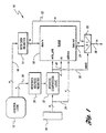
- system 10 is implemented in an application specific integrated circuit (ASIC).
- Control logic 12 communicates with new data register 14 via one or more ( m ) data lines 16.
- New data register 14 communicates with random access memory (RAM) 18 and multiplexer 20 via modifying data lines 22.
- RAM 18 is preferably a single-ported RAM implemented with low-power logic, such as CMOS or the like.
- Multiplexer 20 also communicates with RAM 18 via data output lines 24.
- control logic 12 communicates with a new data address register 26 via new data address lines 28.
- the number of address lines ( n ) will vary according to the size or number of locations of RAM 18 and whether any address and data lines are coincident.
- An address generator 30 communicates with address comparison logic 32 and RAM 18 via address lines 34.
- Address comparison logic 32 communicates with RAM 18 and multiplexer 20 via select/enable line 36.
- Chip select line 40 provides a logic "high level" signal to RAM 18 which is used to enable memory accesses.
- address generator 30 continuously generates an address on address lines 34 to read data from RAM 18. This data is provided to multiplexer 20 via data output lines 24. When no modifying data is present in new data register 14, or when modifying data is present but the address produced by address generator 30 does not match the address in new data address register 26, select/enable line 36 provides a signal to multiplexer 20 such that data read from RAM 18 is passed to system output lines 38.
- control logic 12 is operative to temporarily store the new data in new data register 14 while storing its associated address in new data address register 26.
- Writing (storing) data in new data address register 26 sets a flag which remains set until the data is written to RAM 18.
- New data register 14 provides the new data to RAM 18 and also to multiplexer 20 via modifying data lines 22.
- the new data address is provided to address comparison logic 32 where it is compared to each of the address provided by address generator 30. When the new data address matches the current address provided by address generator 30, address comparison logic asserts select/enable line 36 which is connected to the write enable input of RAM 18 and the select input of multiplexer 20.
- the data present in new data register 14 is written into RAM 18 at the location indicated by the current address provided by address generator 30 (which is the new data address).
- Assertion of select/enable line 36 also provides a signal to multiplexer 20 such that the data in new data register 14 is passed to system output lines 38.
- the new data is provided to the system output lines 38 substantially simultaneously as it is written into RAM 18.
- This allows an uninterrupted data stream at system output lines 38 while also allowing modification of data in memory.
- the only limitation to the implementation illustrated is that it requires a delay between accesses to RAM 18 for the number of clock cycles equal to the size or depth of RAM 18.
- this limitation does not impact system performance.
- system 10 may be used in a space-based, mobile to mobile communications satellite to control data routing and configuration.
- RAM 18 may be a 64x8, for example, which is used to constantly route data.
- the addresses provided by address generator 30 would have sequentially cycling values corresponding to locations zero through sixty-three.
- the value of data on system output lines 38 would then represent another address which would be used to access a second RAM (not specifically illustrated).
- Data stored in RAM 18 may then be used to read call data from various programmable locations in the second RAM. Occasionally, this routing information, i.e. the data in RAM 18, needs to be updated or modified.
- one write to RAM 18 may be completed every sixty-four clock cycles. This limitation does not impact the performance of the system because requests to modify data stored in RAM 18 occur at a rate which is significantly slower than the required delay period.
- FIG. 2 a timing diagram illustrating operation of the system of Figure 1 according to the present invention is shown.
- the timing of a signal representing a current address provided by address generator 30 on address lines 34 is indicated generally by reference numeral 50.
- the values of that signal at various times t 1 through t 4 are indicated generally by A n through A m+2 .
- the timing of a signal representing a new data address provided on new data address lines 28 is indicated generally by reference numeral 52.
- the timing of a signal on select/enable line 36 is indicated generally by reference numeral 54 and the timing of a signal representing data on system output lines 38 is indicated generally by reference numeral 56.
- the values of the data at times t 1 through t 4 are represented by D n through D m+2 , respectively, where ND m+1 represents the value of the new data corresponding to address NA m+1 which is written into location A m+1 during the access cycle between times t 3 and t4.
- data D n+1 is read from memory location A n+1 and provided on system output lines 38 through multiplexer 20 since select/enable line 36 is not asserted as indicated by select/enable timing 54.
- a new data address (NA m+1 ) is placed in new data address register 26 as shown by new address timing 52. Modifying data is also placed in new data register 14 although not specifically illustrated.
- Data continues to be read from RAM 18 until time t 3 where the current address (A m+1 ) is equal to the new data address (NA m+1 ) at which time the select/enable line 36 is asserted as shown by timing 54.
- a memory read is simulated by providing the new data while actually performing a memory write substantially simultaneously to update the current location.
- system output timing 56 data is continuously provided on system output lines.
- FIG. 3 a flowchart illustrating a system and method for simultaneously reading and writing data to a random access memory is shown.
- One of ordinary skill in the art will recognize that the sequence of steps illustrated in the flowchart is not necessarily important to the operation of the present invention but is shown for ease of illustration and description.
- blocks representing operations or steps may be interchanged or performed simultaneously.
- blocks 60 and 62 may be interchanged or performed simultaneously while still achieving the objects of the present invention.
- the operations or steps represented by the blocks of Figure 3 may be performed by hardware, software, or a combination thereof without departing from the spirit or scope of the present invention.
- a modification address corresponding to one of the locations within the RAM is stored as represented by block 60.
- the modification address is stored in a register external to the RAM, such as new data address register 26 ( Figure 1), which is in communication with control logic which controls the memory access.
- the modification address register is preferably implemented on or in combination with an ASIC along with the RAM.
- the modification address is also preferably communicated to comparison logic which determines when the current address corresponds to the modification address.
- Modification or "new" data is stored in a new data register as represented by block 62. Similar to the modification address register, the modification data register is preferably separate from the RAM but may be implemented in the same ASIC.
- a request to read data from the RAM is received as represented by block 64. When the address corresponding to the request to retrieve data is the same as, or corresponds to, the modification address, the modification data is retrieved from the modification data register as represented by block 66. Substantially simultaneously, i.e. during the same memory access, the modification data is stored in the RAM as represented by block 68.
Landscapes
- Engineering & Computer Science (AREA)
- Microelectronics & Electronic Packaging (AREA)
- Radio Relay Systems (AREA)
- Mobile Radio Communication Systems (AREA)
Claims (9)
- Verfahren zur Modifikation und Wiedergewinnung von Daten (D), die in einem Speicher (18) mit wahlfreiem Zugriff an einer Vielzahl von Orten gespeichert sind, die jeweils eine entsprechende Adresse (A) besitzen, wobei das Verfahren die Schritte aufweist:dadurch gekennzeichnet, daßSpeichern (60) einer ersten Adresse (NAm+1) entsprechend einem der Vielzahl von Orten in einem ersten Register (26);Speichern (62) von Modifikationsdaten (NDm+1), die der ersten Adresse (NAm+1) zugeordnet sind, in einem zweiten Register (14);Empfangen (64) einer Anforderung, gespeicherte Daten (D) aus dem Speicher (18) mit wahlfreiem Zugriff an einer zweiten Adresse (A) wiederzugewinnen, die dem einen der Vielzahl von Orten entspricht;Vergleichen (32) der zweiten Adresse (A) mit der ersten Adresse (NAm+1);Wiedergewinnen der gespeicherten Daten (D) aus dem Speicher (18) mit wahlfreiem Zugriff, wenn der Vergleichsschritt anzeigt, daß die erste Adresse (NAm+1) der zweiten Adresse (A) nicht entspricht; undWiedergewinnen (66) der Modifikationsdaten (NDm+1) aus dem zweiten Register (14) und Speichern (68) der Modifikationsdaten (NDm+1) in dem Speicher (18) mit wahlfreiem Zugriff, wenn der Vergleichsschritt anzeigt, daß die erste Adresse (NAm+1) der zweiten Adresse (A) entspricht,
der Speicher (18) mit wahlfreiem Zugriff ein Ein-Port-Speicher mit wahlfreiem Zugriff ist und daß die Modifikationsdaten (NDm+1) in dem zweiten Register (14) solange gespeichert werden, bis die erste Adresse (NAm+1) der zweiten Adresse (A) entspricht. - Verfahren nach Anspruch 1, dadurch gekennzeichnet, daß der Vergleichsschritt (32) beinhaltet zu bestimmen, wenn die erste und die zweite Adresse (NAm+1, A) demselben einen Ort der Vielzahl von Orten entsprechen.
- Verfahren nach Anspruch 2, dadurch gekennzeichnet, daß der Vergleichsschritt (32) beinhaltet zu bestimmen, wenn die erste und die zweite Adresse (NAm+1, A) identisch sind.
- Verfahren nach einem der Ansprüche 1 bis 3, dadurch gekennzeichnet, daß die Schritte des Wiedergewinnens der gespeicherten Daten (D) und des Wiedergewinnens (66) der Modifikationsdaten (NAm+1) wechselseitig ausschließlich durchgeführt werden.
- Verfahren nach Anspruch 2, gekennzeichnet durch wechselseitiges ausschließliches Auswählen (20) entweder der gespeicherten Daten (D) oder der Modifikationsdaten (NDm+1) zur Ausgabe, und zwar auf der Grundlage des Vergleichsschrittes (32).
- Verfahren nach einem der Ansprüche 1 bis 5, dadurch gekennzeichnet, daß das Wiedergewinnen (66) der Modifikationsdaten (NDm+1) aus dem zweiten Register (14) und das Speichern (68) der Modifikationsdaten (NDm+1) in den Speicher (18) mit wahlfreiem Zugriff während eines einzigen Speicherzugriffszyklus durchgeführt werden.
- System (10) zur Modifikation und Wiedergewinnung von Daten (D), die in einem Speicher (18) mit wahlfreiem Zugriff an einer Vielzahl von Orten gespeichert sind, die jeweils eine zugeordnete Adresse (A) aufweisen, wobei das System aufweist:dadurch gekennzeichnet, daßein zweites Register (14), das mit dem Speicher (18) mit wahlfreiem Zugriff in Verbindung steht, und zwar zur Speicherung von Modifikationsdaten (NDm+1);ein erstes Register (26) zur Speicherung einer Modifikationsdatenadresse (NAm+1), die den Modifikationsdaten (NDm+1) zugeordnet ist;Logik (32), die mit dem ersten Register (26) und dem Speicher (18) mit wahlfreiem Zugriff in Verbindung steht, zum Bestimmen, wenn eine Wiedergewinnungsanforderung (64) der Modifikationsdatenadresse (NAm+1) entspricht; undeinen Multiplexer (20), der mit dem Speicher (18) mit wahlfreiem Zugriff, der Logik (32) und dem zweiten Register (14) in Verbindung steht, zum Auswählen entweder der Modifikationsdaten (NDm+1) oder der Daten (D), die in dem Speicher (18) mit wahlfreiem Zugriff gespeichert sind, zur Ausgabe (38), und zwar auf der Grundlage der Bestimmung der Logik (32),
der Speicher (18) mit wahlfreiem Zugriff ein Ein-Port-Speicher (18) ist und daß die Modifikationsdaten (NDm+1) solange in dem zweiten Register (14) gespeichert werden, bis die erste Adresse (NAm+1) der zweiten Adresse (A) entspricht. - System nach Anspruch 7, gekennzeichnet durch einen Adressgenerator (30), der mit der Logik (32) und dem Speicher (18) mit wahlfreiem Zugriff in Verbindung steht, zum Bereitstellen einer Adresse (A), die der Wiedergewinnungsanforderung (64) zugeordnet ist.
- System nach Anspruch 7 oder 8, dadurch gekennzeichnet, daß der Speicher (18) mit wahlfreiem Zugriff, das erste (14) und das zweite (26) Register und die Logik (32) in einer einzelnen integrierten Schaltung (10) implementiert sind.
Applications Claiming Priority (2)
| Application Number | Priority Date | Filing Date | Title |
|---|---|---|---|
| US648792 | 1996-05-16 | ||
| US08/648,792 US5802579A (en) | 1996-05-16 | 1996-05-16 | System and method for simultaneously reading and writing data in a random access memory |
Publications (3)
| Publication Number | Publication Date |
|---|---|
| EP0807935A2 EP0807935A2 (de) | 1997-11-19 |
| EP0807935A3 EP0807935A3 (de) | 1998-11-04 |
| EP0807935B1 true EP0807935B1 (de) | 2002-11-13 |
Family
ID=24602265
Family Applications (1)
| Application Number | Title | Priority Date | Filing Date |
|---|---|---|---|
| EP97107981A Expired - Lifetime EP0807935B1 (de) | 1996-05-16 | 1997-05-16 | Gleichzeitiges Lese- und Schreibeverfahren von Daten in einem RAM-Speicher |
Country Status (3)
| Country | Link |
|---|---|
| US (1) | US5802579A (de) |
| EP (1) | EP0807935B1 (de) |
| DE (1) | DE69716997T2 (de) |
Families Citing this family (26)
| Publication number | Priority date | Publication date | Assignee | Title |
|---|---|---|---|---|
| US6457177B1 (en) * | 1992-05-01 | 2002-09-24 | Digitalconvergence.Com Inc. | Dual port interactive media system |
| JPH1055674A (ja) * | 1996-08-09 | 1998-02-24 | Nec Corp | 半導体記憶装置 |
| JPH1173371A (ja) * | 1997-08-28 | 1999-03-16 | Mitsubishi Electric Corp | レジスタのプロテクト回路 |
| US5978889A (en) * | 1997-11-05 | 1999-11-02 | Timeplex, Inc. | Multiple device data transfer utilizing a multiport memory with opposite oriented memory page rotation for transmission and reception |
| JP3871813B2 (ja) * | 1998-08-10 | 2007-01-24 | 株式会社ルネサステクノロジ | マルチポートメモリ、データプロセッサ及びデータ処理システム |
| US6738072B1 (en) * | 1998-11-09 | 2004-05-18 | Broadcom Corporation | Graphics display system with anti-flutter filtering and vertical scaling feature |
| US7446774B1 (en) | 1998-11-09 | 2008-11-04 | Broadcom Corporation | Video and graphics system with an integrated system bridge controller |
| US6573905B1 (en) | 1999-11-09 | 2003-06-03 | Broadcom Corporation | Video and graphics system with parallel processing of graphics windows |
| US6636222B1 (en) | 1999-11-09 | 2003-10-21 | Broadcom Corporation | Video and graphics system with an MPEG video decoder for concurrent multi-row decoding |
| US6768774B1 (en) | 1998-11-09 | 2004-07-27 | Broadcom Corporation | Video and graphics system with video scaling |
| US6661422B1 (en) | 1998-11-09 | 2003-12-09 | Broadcom Corporation | Video and graphics system with MPEG specific data transfer commands |
| US7982740B2 (en) | 1998-11-09 | 2011-07-19 | Broadcom Corporation | Low resolution graphics mode support using window descriptors |
| US6798420B1 (en) * | 1998-11-09 | 2004-09-28 | Broadcom Corporation | Video and graphics system with a single-port RAM |
| US6853385B1 (en) | 1999-11-09 | 2005-02-08 | Broadcom Corporation | Video, audio and graphics decode, composite and display system |
| US9668011B2 (en) | 2001-02-05 | 2017-05-30 | Avago Technologies General Ip (Singapore) Pte. Ltd. | Single chip set-top box system |
| US6975324B1 (en) | 1999-11-09 | 2005-12-13 | Broadcom Corporation | Video and graphics system with a video transport processor |
| US6144604A (en) * | 1999-11-12 | 2000-11-07 | Haller; Haggai Haim | Simultaneous addressing using single-port RAMs |
| US20020085525A1 (en) * | 2000-12-28 | 2002-07-04 | Junpei Ikegawa | Wireless transmission system |
| US6976114B1 (en) * | 2001-01-25 | 2005-12-13 | Rambus Inc. | Method and apparatus for simultaneous bidirectional signaling in a bus topology |
| US6917536B1 (en) | 2002-09-13 | 2005-07-12 | Lattice Semiconductor Corporation | Memory access circuit and method for reading and writing data with the same clock signal |
| US8063916B2 (en) | 2003-10-22 | 2011-11-22 | Broadcom Corporation | Graphics layer reduction for video composition |
| JP2005259320A (ja) * | 2004-03-15 | 2005-09-22 | Nec Electronics Corp | パーシャル・デュアル・ポート・メモリ及び該メモリを用いた電子機器 |
| JP2005259321A (ja) * | 2004-03-15 | 2005-09-22 | Nec Electronics Corp | フレキシブル・マルチエリア・メモリ及び該メモリを用いた電子機器 |
| US7417907B1 (en) * | 2004-12-23 | 2008-08-26 | Sun Microsystems, Inc. | Systems and methods for resolving memory address collisions |
| JP2007226380A (ja) * | 2006-02-22 | 2007-09-06 | Ricoh Co Ltd | 不揮発性メモリカード |
| US7665003B2 (en) * | 2006-12-15 | 2010-02-16 | Qualcomm Incorporated | Method and device for testing memory |
Family Cites Families (11)
| Publication number | Priority date | Publication date | Assignee | Title |
|---|---|---|---|---|
| US4573116A (en) * | 1983-12-20 | 1986-02-25 | Honeywell Information Systems Inc. | Multiword data register array having simultaneous read-write capability |
| JP2615088B2 (ja) * | 1987-11-06 | 1997-05-28 | 株式会社日立製作所 | 半導体記憶装置 |
| US4933909A (en) * | 1988-12-19 | 1990-06-12 | Bull Hn Information Systems Inc. | Dual read/write register file memory |
| US5001671A (en) * | 1989-06-27 | 1991-03-19 | Vitelic Corporation | Controller for dual ported memory |
| WO1991007754A1 (en) * | 1989-11-13 | 1991-05-30 | Cray Research, Inc. | Read-while-write-memory |
| US5371877A (en) * | 1991-12-31 | 1994-12-06 | Apple Computer, Inc. | Apparatus for alternatively accessing single port random access memories to implement dual port first-in first-out memory |
| JP4018159B2 (ja) * | 1993-06-28 | 2007-12-05 | 株式会社ルネサステクノロジ | 半導体集積回路 |
| US5375089A (en) * | 1993-10-05 | 1994-12-20 | Advanced Micro Devices, Inc. | Plural port memory system utilizing a memory having a read port and a write port |
| US5479128A (en) * | 1994-03-16 | 1995-12-26 | Industrial Technology Research Institute | Single ram multiple-delay variable delay circuit |
| US5666494A (en) * | 1995-03-31 | 1997-09-09 | Samsung Electronics Co., Ltd. | Queue management mechanism which allows entries to be processed in any order |
| US5568443A (en) * | 1995-09-08 | 1996-10-22 | Smithills Multimedia Systems, Inc. | Combination dual-port random access memory and multiple first-in-first-out (FIFO) buffer memories |
-
1996
- 1996-05-16 US US08/648,792 patent/US5802579A/en not_active Expired - Lifetime
-
1997
- 1997-05-16 DE DE69716997T patent/DE69716997T2/de not_active Expired - Lifetime
- 1997-05-16 EP EP97107981A patent/EP0807935B1/de not_active Expired - Lifetime
Also Published As
| Publication number | Publication date |
|---|---|
| EP0807935A2 (de) | 1997-11-19 |
| DE69716997T2 (de) | 2003-07-17 |
| US5802579A (en) | 1998-09-01 |
| DE69716997D1 (de) | 2002-12-19 |
| EP0807935A3 (de) | 1998-11-04 |
Similar Documents
| Publication | Publication Date | Title |
|---|---|---|
| EP0807935B1 (de) | Gleichzeitiges Lese- und Schreibeverfahren von Daten in einem RAM-Speicher | |
| US5838631A (en) | Fully synchronous pipelined ram | |
| US5781558A (en) | Diagnostic memory access | |
| US4954988A (en) | Memory device wherein a shadow register corresponds to each memory cell | |
| US7796462B2 (en) | Data flow control in multiple independent port | |
| US5956748A (en) | Asynchronous, dual-port, RAM-based FIFO with bi-directional address synchronization | |
| KR100915554B1 (ko) | 반도체기억장치 | |
| KR100254752B1 (ko) | 메모리 확장을 위한 로직을 갖는 동기식 sram | |
| JPH05210567A (ja) | メモリ装置及びメモリのデータ読取り/書込み方法 | |
| US6205084B1 (en) | Burst mode flash memory | |
| US5787273A (en) | Multiple parallel identical finite state machines which share combinatorial logic | |
| JPH0383299A (ja) | 半導体記憶装置 | |
| KR100377708B1 (ko) | 저소비 전력화가 가능한 파이프라인 방식의 반도체 기억장치 | |
| EP0493138B1 (de) | Speicherschaltung | |
| US5577228A (en) | Digital circuit for performing multicycle addressing in a digital memory | |
| JPH07248962A (ja) | ランダムアクセスメモリのメモリチップ拡張制御方法及び装置 | |
| EP1416494A2 (de) | Halbleiterspeicheranordnung zur Hochgeschwindigkeitsverarbeitung | |
| US6445634B2 (en) | Serial access memory and data write/read method | |
| JP2954286B2 (ja) | 半導体記憶装置 | |
| US7353330B2 (en) | Method and apparatus for performing repeated content addressable memory searches | |
| US6757752B2 (en) | Micro controller development system | |
| US6744833B1 (en) | Data resynchronization between modules sharing a common clock | |
| JP3003283B2 (ja) | 半導体記憶装置 | |
| KR100281548B1 (ko) | 선입선출장치 | |
| JPH05189340A (ja) | データ遅延制御方式 |
Legal Events
| Date | Code | Title | Description |
|---|---|---|---|
| PUAI | Public reference made under article 153(3) epc to a published international application that has entered the european phase |
Free format text: ORIGINAL CODE: 0009012 |
|
| AK | Designated contracting states |
Kind code of ref document: A2 Designated state(s): DE FR GB |
|
| PUAL | Search report despatched |
Free format text: ORIGINAL CODE: 0009013 |
|
| AK | Designated contracting states |
Kind code of ref document: A3 Designated state(s): DE FR GB |
|
| RAP1 | Party data changed (applicant data changed or rights of an application transferred) |
Owner name: HUGHES ELECTRONICS CORPORATION |
|
| 17P | Request for examination filed |
Effective date: 19990416 |
|
| GRAG | Despatch of communication of intention to grant |
Free format text: ORIGINAL CODE: EPIDOS AGRA |
|
| 17Q | First examination report despatched |
Effective date: 20020411 |
|
| GRAG | Despatch of communication of intention to grant |
Free format text: ORIGINAL CODE: EPIDOS AGRA |
|
| GRAH | Despatch of communication of intention to grant a patent |
Free format text: ORIGINAL CODE: EPIDOS IGRA |
|
| GRAH | Despatch of communication of intention to grant a patent |
Free format text: ORIGINAL CODE: EPIDOS IGRA |
|
| GRAA | (expected) grant |
Free format text: ORIGINAL CODE: 0009210 |
|
| AK | Designated contracting states |
Kind code of ref document: B1 Designated state(s): DE FR GB |
|
| REG | Reference to a national code |
Ref country code: GB Ref legal event code: FG4D |
|
| REF | Corresponds to: |
Ref document number: 69716997 Country of ref document: DE Date of ref document: 20021219 |
|
| ET | Fr: translation filed | ||
| PLBE | No opposition filed within time limit |
Free format text: ORIGINAL CODE: 0009261 |
|
| STAA | Information on the status of an ep patent application or granted ep patent |
Free format text: STATUS: NO OPPOSITION FILED WITHIN TIME LIMIT |
|
| 26N | No opposition filed |
Effective date: 20030814 |
|
| REG | Reference to a national code |
Ref country code: FR Ref legal event code: PLFP Year of fee payment: 20 |
|
| PGFP | Annual fee paid to national office [announced via postgrant information from national office to epo] |
Ref country code: GB Payment date: 20160527 Year of fee payment: 20 Ref country code: DE Payment date: 20160527 Year of fee payment: 20 |
|
| PGFP | Annual fee paid to national office [announced via postgrant information from national office to epo] |
Ref country code: FR Payment date: 20160530 Year of fee payment: 20 |
|
| REG | Reference to a national code |
Ref country code: DE Ref legal event code: R071 Ref document number: 69716997 Country of ref document: DE |
|
| REG | Reference to a national code |
Ref country code: GB Ref legal event code: PE20 Expiry date: 20170515 |
|
| PG25 | Lapsed in a contracting state [announced via postgrant information from national office to epo] |
Ref country code: GB Free format text: LAPSE BECAUSE OF EXPIRATION OF PROTECTION Effective date: 20170515 |