EP0802706A1 - Uni-Kontaktfläche für oberflächenmontierte Bauteilpackung - Google Patents
Uni-Kontaktfläche für oberflächenmontierte Bauteilpackung Download PDFInfo
- Publication number
- EP0802706A1 EP0802706A1 EP97302410A EP97302410A EP0802706A1 EP 0802706 A1 EP0802706 A1 EP 0802706A1 EP 97302410 A EP97302410 A EP 97302410A EP 97302410 A EP97302410 A EP 97302410A EP 0802706 A1 EP0802706 A1 EP 0802706A1
- Authority
- EP
- European Patent Office
- Prior art keywords
- distance
- surface mount
- pad
- terminals
- uni
- Prior art date
- Legal status (The legal status is an assumption and is not a legal conclusion. Google has not performed a legal analysis and makes no representation as to the accuracy of the status listed.)
- Withdrawn
Links
Images
Classifications
-
- H—ELECTRICITY
- H05—ELECTRIC TECHNIQUES NOT OTHERWISE PROVIDED FOR
- H05K—PRINTED CIRCUITS; CASINGS OR CONSTRUCTIONAL DETAILS OF ELECTRIC APPARATUS; MANUFACTURE OF ASSEMBLAGES OF ELECTRICAL COMPONENTS
- H05K3/00—Apparatus or processes for manufacturing printed circuits
- H05K3/30—Assembling printed circuits with electric components, e.g. with resistors
- H05K3/32—Assembling printed circuits with electric components, e.g. with resistors electrically connecting electric components or wires to printed circuits
- H05K3/34—Assembling printed circuits with electric components, e.g. with resistors electrically connecting electric components or wires to printed circuits by soldering
- H05K3/341—Surface mounted components
- H05K3/3431—Leadless components
- H05K3/3442—Leadless components having edge contacts, e.g. leadless chip capacitors, chip carriers
-
- H—ELECTRICITY
- H05—ELECTRIC TECHNIQUES NOT OTHERWISE PROVIDED FOR
- H05K—PRINTED CIRCUITS; CASINGS OR CONSTRUCTIONAL DETAILS OF ELECTRIC APPARATUS; MANUFACTURE OF ASSEMBLAGES OF ELECTRICAL COMPONENTS
- H05K1/00—Printed circuits
- H05K1/02—Details
- H05K1/0286—Programmable, customizable or modifiable circuits
- H05K1/0295—Programmable, customizable or modifiable circuits adapted for choosing between different types or different locations of mounted components
-
- H—ELECTRICITY
- H05—ELECTRIC TECHNIQUES NOT OTHERWISE PROVIDED FOR
- H05K—PRINTED CIRCUITS; CASINGS OR CONSTRUCTIONAL DETAILS OF ELECTRIC APPARATUS; MANUFACTURE OF ASSEMBLAGES OF ELECTRICAL COMPONENTS
- H05K1/00—Printed circuits
- H05K1/02—Details
- H05K1/11—Printed elements for providing electric connections to or between printed circuits
- H05K1/111—Pads for surface mounting, e.g. lay-out
-
- H—ELECTRICITY
- H05—ELECTRIC TECHNIQUES NOT OTHERWISE PROVIDED FOR
- H05K—PRINTED CIRCUITS; CASINGS OR CONSTRUCTIONAL DETAILS OF ELECTRIC APPARATUS; MANUFACTURE OF ASSEMBLAGES OF ELECTRICAL COMPONENTS
- H05K2201/00—Indexing scheme relating to printed circuits covered by H05K1/00
- H05K2201/09—Shape and layout
- H05K2201/09818—Shape or layout details not covered by a single group of H05K2201/09009 - H05K2201/09809
- H05K2201/09954—More mounting possibilities, e.g. on same place of PCB, or by using different sets of edge pads
-
- H—ELECTRICITY
- H05—ELECTRIC TECHNIQUES NOT OTHERWISE PROVIDED FOR
- H05K—PRINTED CIRCUITS; CASINGS OR CONSTRUCTIONAL DETAILS OF ELECTRIC APPARATUS; MANUFACTURE OF ASSEMBLAGES OF ELECTRICAL COMPONENTS
- H05K2201/00—Indexing scheme relating to printed circuits covered by H05K1/00
- H05K2201/10—Details of components or other objects attached to or integrated in a printed circuit board
- H05K2201/10613—Details of electrical connections of non-printed components, e.g. special leads
- H05K2201/10621—Components characterised by their electrical contacts
- H05K2201/10636—Leadless chip, e.g. chip capacitor or resistor
-
- Y—GENERAL TAGGING OF NEW TECHNOLOGICAL DEVELOPMENTS; GENERAL TAGGING OF CROSS-SECTIONAL TECHNOLOGIES SPANNING OVER SEVERAL SECTIONS OF THE IPC; TECHNICAL SUBJECTS COVERED BY FORMER USPC CROSS-REFERENCE ART COLLECTIONS [XRACs] AND DIGESTS
- Y02—TECHNOLOGIES OR APPLICATIONS FOR MITIGATION OR ADAPTATION AGAINST CLIMATE CHANGE
- Y02P—CLIMATE CHANGE MITIGATION TECHNOLOGIES IN THE PRODUCTION OR PROCESSING OF GOODS
- Y02P70/00—Climate change mitigation technologies in the production process for final industrial or consumer products
- Y02P70/50—Manufacturing or production processes characterised by the final manufactured product
Definitions
- This invention relates to electrical component surface mount technology, and in particular to the bonding pads on printed wiring boards which support the components.
- PWBs printed wiring boards
- This technology provided tremendous advantages over point-to-point wiring, but it still used a relatively large area because the discrete components were essentially designed for point-to point wiring assembly.
- solder paste is screened by a squeegee through a stencil, typically stainless steel, which has photolithographically defined holes which correspond to pad areas on the PWB.
- the solder paste is a mixture of solder particles of predetermined composition and melting point. The particles are contained in a viscous medium of soldering flux, solvent, and viscousifiers or other agents which improve the screening operation and provide a tacky surface onto which the terminals of the surface mount component are set.
- the components are usually presented in a tape or cartridge and a programmed pick-and-place machine lifts them from their container with a vacuum chuck, orients and aligns them over the correct pads, and places them onto the soldering paste.
- the viscous flux holds the components in place over the pads which are typically solder coated copper.
- the terminals on each end of the surface mount component are also solder coated and the flux in the paste dissolves any oxide which may be present and ensures that the solder particles will wet the component terminals and their corresponding pads.
- This reflow process is done in an oven and the solder is usually a tin-lead alloy, near the eutectic composition, which melts at 183 degrees centigrade. Other alloy compositions can be used to melt at different temperatures which are well known in the art.
- the present invention relates to a uni-pad which is a structure on the surface of a PWB comprising a pair of complimentary pads, arranged on an axis, whose dimensions are selected to support the terminals of a plurality of surface mount component sizes.
- the width of each pad is the width of the widest anticipated surface mount component which may be substituted.
- a first distance, denoting the separation of the inner edges of each pad, is selected as the minimum distance between inner edges of the terminals of the anticipated surface mount components.
- a second distance, denoting the distance between outer edges of the complimentary pads is selected as the maximum distance between outer edges of the terminals of anticipated surface mount components.
- a manufacturing tolerance may be incorporated into each of these dimensions.
- a manufacturing tolerance may be subtracted from that distance.
- a manufacturing tolerance may be added for the second distance between the outer edges of the complimentary pads and the width.
- a single uni-pad may thus support surface mount components of varying sizes.
- a PWB supports at least one uni-pad whose structure and dimensions are described above so that the uni-pad may support varying sizes of surface mount components.
- the complimentary pads are conductors, typically a metal such as copper which may be solder coated.
- the PWB may also support metal traces which interconnect the uni-pad to other structures on the PWB.
- the advantage of the uni-pad structure is that a variety of surface mount component sizes may be accommodated by one PWB design to improve the selection of the components for price, availability, function, or reliability. The cost and delay of redesigning and manufacturing a new PWB are avoided.
- a printed wiring board adapted to support surface mount components comprising:
- a printed wiring board adapted to support surface mount components of at least two different sizes comprising:
- a method of designing a uni-pad described herein which supports terminals of at least two surface mount components of different sizes comprising:
- a uni-pad for a printed wiring board to support the terminals of one or more surface mount components and providing interconnecting electrical surfaces cooperating with other structures on said board comprising a pair of complementary pads, wherein each complementary pad has common width, and inner edge, and an outer edge; and the distance between inner and outer edges being adapted to support the terminals of at least one surface mount component.
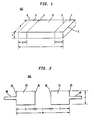
- a typical surface mount component 100, having a width, W, a height, H, and a length, L.
- Each end of the surface mount component is comprised of a terminal 4 having inner edge 6 and an outer edge 8. The inner and outer edges of each terminal are separated by a distance, A.
- the interior of the surface mount component is body 12 which contains a discrete electrical component such as a resistor, capacitor, inductor, or diode.
- the terminals are metallic conductors and are typically coated with solder, for example a solder of a lead-tin alloy of a specific ratio and melting point.
- a uni-pad, 200 which is a structure comprising a pair of complimentary pads 20, supported by an upper or a lower surface of a PWB.
- Each pad has an inner edge 26 and an outer edge 28 separated by a distance, D.
- the inner edges are separated by a distance, E, which is a first distance.
- the distance between the outer edges, shown as M, is a second distance.
- the pads function to support a surface mount component. They are typically made of an electrical conductor and they are formed by photolithographic processes which are well known.
- the conductor may be a noble metal, or alloy thereof, such as gold, palladium, silver or their alloys.
- the conductor also may be a refractory metal such as titanium or tungsten or silicides thereof. These metals are typical where the PWB substrate is made of a ceramic or silicon.
- the most common substrate is an organic material which supports a foil of copper which is photolithographically defined to form complimentary pads 20 and other structures such as traces 40 which emanate from each pad 20, and other conductors, pads, terminals, and the like, which are common to PWBs.
- the goal of the uni-pad is to accommodate at least two standard sizes of surface mount components having dimensions W, A, and L as shown in Fig. 1. This will provide the advantage of being able to switch components for price, availability, or design changes for performance, upgrades, and reliability without the need to redesign the PWB. This provides a competitive advantage in terms of costs saved and design time.
- Several conditions must be met to accomplish this: first, the terminals 4 of each surface mount component size which is anticipated as a substitute must be sufficiently supported by the uni-pad to ensure reliable bonding; second, manufacturing tolerances arising form component size, placement, and pad etching dimensions must be considered, especially for the smaller components where the A dimension in Fig. 1 is 15 mils and L is only 60 mils.
- Manufacturing tolerances for component dimension, placement, and pad etching may also be added to K. A typical tolerance to accommodate these effects may be 2.5 mils.
- E [L-2A] min .
- the manufacturing tolerances must be subtracted from the first distance.
- the solution is to lessen the contact area below the component, so the dimension E may be increased by 6 mils. This compensation in the design dimensions has been experimentally determined to eliminate "tombstoning" yet provide a reliable bond to the PWB.
- the design process for a uni-pad therefore comprises the steps of: selecting a width which is the maximum width of anticipated surface mount components, selecting a first distance which is the minimum of the terminal inner edge distance of the anticipated surface mount components, and selecting a second distance which is the maximum of the terminal outer edges distance of anticipated surface mount components.
- a manufacturing tolerance to account for dimensional variations in the components, pick-and-place errors, and pad etching errors may be used to adjust each dimension. The adjustment is added to the width and second dimension and subtracted from the first dimension. Further, a compensation in the first distance may be added for the case of small surface mount components to eliminate the effect of "tombstoning".
Landscapes
- Engineering & Computer Science (AREA)
- Microelectronics & Electronic Packaging (AREA)
- Manufacturing & Machinery (AREA)
- Electric Connection Of Electric Components To Printed Circuits (AREA)
- Manufacturing Of Printed Wiring (AREA)
- Lead Frames For Integrated Circuits (AREA)
Applications Claiming Priority (2)
| Application Number | Priority Date | Filing Date | Title |
|---|---|---|---|
| US63448696A | 1996-04-18 | 1996-04-18 | |
| US634486 | 1996-04-18 |
Publications (1)
| Publication Number | Publication Date |
|---|---|
| EP0802706A1 true EP0802706A1 (de) | 1997-10-22 |
Family
ID=24544002
Family Applications (1)
| Application Number | Title | Priority Date | Filing Date |
|---|---|---|---|
| EP97302410A Withdrawn EP0802706A1 (de) | 1996-04-18 | 1997-04-08 | Uni-Kontaktfläche für oberflächenmontierte Bauteilpackung |
Country Status (4)
| Country | Link |
|---|---|
| EP (1) | EP0802706A1 (de) |
| JP (1) | JPH1041614A (de) |
| AU (1) | AU717601B2 (de) |
| CA (1) | CA2200122C (de) |
Cited By (1)
| Publication number | Priority date | Publication date | Assignee | Title |
|---|---|---|---|---|
| ES2154593A1 (es) * | 1999-06-08 | 2001-04-01 | Mecanismos Aux Es Ind S L | Diseño de patterns de componentes electronicos sobre una capa de cobre de 400 micras en los circuitos impresos. |
Families Citing this family (2)
| Publication number | Priority date | Publication date | Assignee | Title |
|---|---|---|---|---|
| JP2003017840A (ja) * | 2001-06-29 | 2003-01-17 | Toshiba Corp | プリント基板 |
| JP4852111B2 (ja) * | 2009-01-15 | 2012-01-11 | 三菱電機株式会社 | プリント配線基板 |
Citations (5)
| Publication number | Priority date | Publication date | Assignee | Title |
|---|---|---|---|---|
| US4645114A (en) * | 1985-06-17 | 1987-02-24 | Northern Telecom Limited | Shaped solder pad for surface mounting electronic devices and a surface mounting position incorporating such shaped pads |
| JPS6464393A (en) * | 1987-09-04 | 1989-03-10 | Mitsubishi Electric Corp | Mounting apparatus for circuit device |
| JPH05102648A (ja) * | 1991-10-04 | 1993-04-23 | Hitachi Ltd | プリント基板 |
| US5303122A (en) * | 1991-10-31 | 1994-04-12 | Ford Motor Company | Printed circuit board having a commonized mounting pad which different sized surface mounted devices can be mounted |
| JPH0864956A (ja) * | 1994-08-23 | 1996-03-08 | Hitachi Ltd | 制御装置 |
-
1997
- 1997-03-17 CA CA002200122A patent/CA2200122C/en not_active Expired - Fee Related
- 1997-04-08 EP EP97302410A patent/EP0802706A1/de not_active Withdrawn
- 1997-04-14 AU AU17868/97A patent/AU717601B2/en not_active Ceased
- 1997-04-18 JP JP9101138A patent/JPH1041614A/ja active Pending
Patent Citations (5)
| Publication number | Priority date | Publication date | Assignee | Title |
|---|---|---|---|---|
| US4645114A (en) * | 1985-06-17 | 1987-02-24 | Northern Telecom Limited | Shaped solder pad for surface mounting electronic devices and a surface mounting position incorporating such shaped pads |
| JPS6464393A (en) * | 1987-09-04 | 1989-03-10 | Mitsubishi Electric Corp | Mounting apparatus for circuit device |
| JPH05102648A (ja) * | 1991-10-04 | 1993-04-23 | Hitachi Ltd | プリント基板 |
| US5303122A (en) * | 1991-10-31 | 1994-04-12 | Ford Motor Company | Printed circuit board having a commonized mounting pad which different sized surface mounted devices can be mounted |
| JPH0864956A (ja) * | 1994-08-23 | 1996-03-08 | Hitachi Ltd | 制御装置 |
Non-Patent Citations (3)
| Title |
|---|
| PATENT ABSTRACTS OF JAPAN vol. 13, no. 277 (E - 778) 26 June 1989 (1989-06-26) * |
| PATENT ABSTRACTS OF JAPAN vol. 17, no. 453 (E - 1417) 19 August 1993 (1993-08-19) * |
| PATENT ABSTRACTS OF JAPAN vol. 96, no. 7 31 July 1996 (1996-07-31) * |
Cited By (1)
| Publication number | Priority date | Publication date | Assignee | Title |
|---|---|---|---|---|
| ES2154593A1 (es) * | 1999-06-08 | 2001-04-01 | Mecanismos Aux Es Ind S L | Diseño de patterns de componentes electronicos sobre una capa de cobre de 400 micras en los circuitos impresos. |
Also Published As
| Publication number | Publication date |
|---|---|
| AU717601B2 (en) | 2000-03-30 |
| CA2200122A1 (en) | 1997-10-18 |
| CA2200122C (en) | 2001-10-30 |
| AU1786897A (en) | 1997-10-23 |
| JPH1041614A (ja) | 1998-02-13 |
Similar Documents
| Publication | Publication Date | Title |
|---|---|---|
| US5401910A (en) | Electronic component | |
| US5973932A (en) | Soldered component bonding in a printed circuit assembly | |
| EP0947125B1 (de) | Verfahren zum herstellen einer leiterplatteranordnung mit zinn/bleischicht | |
| US6264093B1 (en) | Lead-free solder process for printed wiring boards | |
| JP4181759B2 (ja) | 電子部品の実装方法および実装構造体の製造方法 | |
| US20090199400A1 (en) | Electronic apparatus and method of manufacturing the same | |
| JP2000509203A (ja) | はんだバンプの形成方法 | |
| US4972989A (en) | Through the lead soldering | |
| TW590836B (en) | Method of mounting electronic parts with Sn-Zn solder free of Pb without reduction in bonding strength | |
| JP2639280B2 (ja) | 高密度回路モジュールの製造方法 | |
| CA2200122C (en) | Uni-pad surface mount component package | |
| JP4143280B2 (ja) | 実装構造体、該実装構造体の製造方法、印刷用マスク、および印刷方法 | |
| EP1103995A1 (de) | Elektronikbauteil und dieser enthaltendes elektronisches gerät und herstellungsverfahren | |
| EP0568087A2 (de) | Einbau von elektronischen Komponenten auf Montageplatten mit Hilfe der Reflow-Technik | |
| JP3189209B2 (ja) | 電子部品の表面実装方法 | |
| JPH04243187A (ja) | プリント基板 | |
| JPS6333319B2 (de) | ||
| JPH0536302Y2 (de) | ||
| JPH0774448A (ja) | プリント配線板 | |
| JPH11177224A (ja) | メタルマスク及びプリント配線板 | |
| JPH05259632A (ja) | プリント配線板およびその製造方法 | |
| JPH0547997B2 (de) | ||
| JPH07106751A (ja) | 耐ストレスチップ部品及びその実装方法 | |
| JPH0729662Y2 (ja) | 面実装型電子部品を使用した基板装置 | |
| JPH05327164A (ja) | 面実装用電子部品の端子構造 |
Legal Events
| Date | Code | Title | Description |
|---|---|---|---|
| PUAI | Public reference made under article 153(3) epc to a published international application that has entered the european phase |
Free format text: ORIGINAL CODE: 0009012 |
|
| AK | Designated contracting states |
Kind code of ref document: A1 Designated state(s): DE ES FR GB IT |
|
| 17P | Request for examination filed |
Effective date: 19980409 |
|
| 17Q | First examination report despatched |
Effective date: 20001005 |
|
| STAA | Information on the status of an ep patent application or granted ep patent |
Free format text: STATUS: THE APPLICATION IS DEEMED TO BE WITHDRAWN |
|
| 18D | Application deemed to be withdrawn |
Effective date: 20030325 |