EP0801418A2 - Herstellungsverfahren einer T-förmigen Gate-Elektrode in einem Halbleiterbauelement, und die T-förmige Gate-Elektrode - Google Patents
Herstellungsverfahren einer T-förmigen Gate-Elektrode in einem Halbleiterbauelement, und die T-förmige Gate-Elektrode Download PDFInfo
- Publication number
- EP0801418A2 EP0801418A2 EP97105617A EP97105617A EP0801418A2 EP 0801418 A2 EP0801418 A2 EP 0801418A2 EP 97105617 A EP97105617 A EP 97105617A EP 97105617 A EP97105617 A EP 97105617A EP 0801418 A2 EP0801418 A2 EP 0801418A2
- Authority
- EP
- European Patent Office
- Prior art keywords
- resist
- gate electrode
- shaped gate
- semiconductor device
- forming
- Prior art date
- Legal status (The legal status is an assumption and is not a legal conclusion. Google has not performed a legal analysis and makes no representation as to the accuracy of the status listed.)
- Granted
Links
Images
Classifications
-
- H—ELECTRICITY
- H10—SEMICONDUCTOR DEVICES; ELECTRIC SOLID-STATE DEVICES NOT OTHERWISE PROVIDED FOR
- H10D—INORGANIC ELECTRIC SEMICONDUCTOR DEVICES
- H10D30/00—Field-effect transistors [FET]
- H10D30/01—Manufacture or treatment
- H10D30/061—Manufacture or treatment of FETs having Schottky gates
- H10D30/0612—Manufacture or treatment of FETs having Schottky gates of lateral single-gate Schottky FETs
-
- H—ELECTRICITY
- H10—SEMICONDUCTOR DEVICES; ELECTRIC SOLID-STATE DEVICES NOT OTHERWISE PROVIDED FOR
- H10D—INORGANIC ELECTRIC SEMICONDUCTOR DEVICES
- H10D64/00—Electrodes of devices having potential barriers
- H10D64/01—Manufacture or treatment
- H10D64/012—Manufacture or treatment of electrodes comprising a Schottky barrier to a semiconductor
- H10D64/0124—Manufacture or treatment of electrodes comprising a Schottky barrier to a semiconductor to Group III-V semiconductors
- H10D64/0125—Manufacture or treatment of electrodes comprising a Schottky barrier to a semiconductor to Group III-V semiconductors characterised by the sectional shape, e.g. T or inverted T
-
- H—ELECTRICITY
- H10—SEMICONDUCTOR DEVICES; ELECTRIC SOLID-STATE DEVICES NOT OTHERWISE PROVIDED FOR
- H10P—GENERIC PROCESSES OR APPARATUS FOR THE MANUFACTURE OR TREATMENT OF DEVICES COVERED BY CLASS H10
- H10P76/00—Manufacture or treatment of masks on semiconductor bodies, e.g. by lithography or photolithography
- H10P76/20—Manufacture or treatment of masks on semiconductor bodies, e.g. by lithography or photolithography of masks comprising organic materials
- H10P76/202—Manufacture or treatment of masks on semiconductor bodies, e.g. by lithography or photolithography of masks comprising organic materials for lift-off processes
-
- Y—GENERAL TAGGING OF NEW TECHNOLOGICAL DEVELOPMENTS; GENERAL TAGGING OF CROSS-SECTIONAL TECHNOLOGIES SPANNING OVER SEVERAL SECTIONS OF THE IPC; TECHNICAL SUBJECTS COVERED BY FORMER USPC CROSS-REFERENCE ART COLLECTIONS [XRACs] AND DIGESTS
- Y10—TECHNICAL SUBJECTS COVERED BY FORMER USPC
- Y10S—TECHNICAL SUBJECTS COVERED BY FORMER USPC CROSS-REFERENCE ART COLLECTIONS [XRACs] AND DIGESTS
- Y10S438/00—Semiconductor device manufacturing: process
- Y10S438/942—Masking
- Y10S438/948—Radiation resist
- Y10S438/949—Energy beam treating radiation resist on semiconductor
-
- Y—GENERAL TAGGING OF NEW TECHNOLOGICAL DEVELOPMENTS; GENERAL TAGGING OF CROSS-SECTIONAL TECHNOLOGIES SPANNING OVER SEVERAL SECTIONS OF THE IPC; TECHNICAL SUBJECTS COVERED BY FORMER USPC CROSS-REFERENCE ART COLLECTIONS [XRACs] AND DIGESTS
- Y10—TECHNICAL SUBJECTS COVERED BY FORMER USPC
- Y10S—TECHNICAL SUBJECTS COVERED BY FORMER USPC CROSS-REFERENCE ART COLLECTIONS [XRACs] AND DIGESTS
- Y10S438/00—Semiconductor device manufacturing: process
- Y10S438/942—Masking
- Y10S438/948—Radiation resist
- Y10S438/951—Lift-off
Definitions
- the present invention relates to a manufacturing method of T-shaped gate electrode in a semiconductor device, comprising the steps of: 1) forming a first resist on a semiconductor substrate on which source and drain electrodes are provided; 2) forming a first gate opening on said first resist between said source and drain electrodes; 3) deforming said first resist by baking; 4) forming a second resist overlaying said first resist and said first gate opening; 5) forming a second gate opening on said second resist above said first gate opening, said second gate opening being larger than said first gate opening; 6) depositing electrode metal for forming the T-shaped gate electrode on said second gate opening; and 7) removing said first and second resist.
- the present invention also relates to T-shaped gate electrode in a semiconductor device.
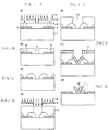
- Figs. 2A to 2G show a method for forming a T-shaped gate electrode with a conventional two resist layers. As shown in Fig. 2A, a source/drain electrode 2 is formed on a semiconductor substrate 1, and a first resist 3 is subsequently formed. As shown in Fig.
- a first gate opening 6 is subsequently formed by developing the exposed first resist 3.
- the first resist 3 is deformed by baking, at 180°C for 3 minutes for example, and as shown in Fig. 2D, a second resist 7 is formed, and exposure light 9 is emitted through a photomask 8 to expose the second resist 7.
- a second gate opening 10 is formed by developing the exposed second resist 7.
- gate electrode metal 11 is deposited on the overall surface of the second resist 7, and subsequently, as shown in Fig.
- the gate electrode metal 11 is removed to produce a T-shaped gate electrode.
- it is essential to bake the first resist 3 to cure (step shown in Fig. 2C) after patterning the first resist 3 so that the width of the first gate opening 6 in the first resist 3 is constant after the baking step.
- the baking step causes deformation of the first resist 3, which greatly affects the shape of the finally obtained gate electrode.
- a rise angle ⁇ (shown in Fig. 2G) of the gate electrode is determined by the shape of the first resist 3.
- the rise angle ⁇ decreases, so the distance between the gate electrode 12 and the semiconductor substrate 1 except for contact portion thereof narrows. Therefore, to obtain a T-shaped gate electrode in a semiconductor device which has a large rise angle, particularly 30 degrees or more, is difficult.
- the space between the electrode 12 and the semiconductor 1 has capacitance, which is so-called parasitic capacitance.
- Enlarging the distance between the gate electrode 12 and the semiconductor substrate 1 reduces parasitic capacitance i.e., improve transistor characteristics such as a cut-off frequency, and so forth. In other words, the deformation of the first resist 3 increases parasitic capacitance i.e., deteriorate the transistor characteristics.
- the ultraviolet curing technique As means to prevent the deformation of the first resist 3, it is possible to use an ultraviolet curing technique which emits ultraviolet light to the first resist 3 to cure in advance after the step shown in Fig. 2B.
- the ultraviolet curing technique is not preferable because it requires expensive equipment and long processing time, which increases a cost of producing semiconductor devices.
- the foregoing object is achieved through the provision of a manufacturing method above mentioned kind, which is characterized in that a pair of dummy openings are formed on said first resist in proximity to both sides of said first gate opening, and a pair of first resist convex portions are formed when said first resist are deformed by baking.
- a lift-off technique may be performed to remove said first and second resist.
- said first resist convex portions have a pattern such that said T-shaped gate electrode is formed being analogous to V-shape.
- the T-shaped gate electrode may be formed such that a rise angle thereof is 30 degrees or more with respect to the surface of said semiconductor substrate. Preferably, said rise angle of said T-shaped gate electrode is 45 degrees or more.
- the second resist may be baked at a temperature lower than a temperature at which the first resist is baked.
- the semiconductor device which has the T-shaped gate electrode may be a field effect transistor.
- the foregoing object is achieved through the provision of a T-shaped gate electrode in a semiconductor device, which is characterized in that the T-shaped gate electrode is analogous to V-shape and a rise angle thereof is 30 degrees or more with respect to the surface of said semiconductor substrate. Preferably, the rise angle thereof is 45 degrees or more.
- the semiconductor device in this aspect of the invention may be a field effect transistor as well.
- the dummy openings in proximity to both sides of the first gate opening, deformation of the first resist can be prevented, and the first resist convex portions rising steeply can be formed between the first gate opening and the dummy openings.
- the T-shaped gate electrode which has a large rise angle with respect to the surface of the semiconductor substrate.
- the reason why the second resist is preferably baked at a temperature lower than a temperature at which the first resist is baked is to prevent intermixing of the first resist and the second resist while they are being baked, and to prevent deformation of the first resist.
- the distance between the gate electrode and the semiconductor substrate except for contact portion thereof can be increased, so that parasitic capacitance can be reduced, and a field-effect transistor with preferable characteristics such as a cut-off frequency and so forth can finally be obtained.
- the parasitic capacitance can further be reduced to improve field-effect transistor characteristics.
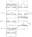
- Figs. 1A to 1G show one embodiment of the present invention.
- the same reference numerals as those in Figs. 2A to 2G denote the same or corresponding portions.
- a positive photoresist such as PFi26A (produced by Sumitomo Chemical Co., Ltd.) is coated to be approximately 1 ⁇ m thick by spin coating, and the coated photoresist is baked at 90°C for 90 seconds to form a first resist 3.
- an i-line stepper to emit exposure light 5 onto the first resist 3 through a photo mask 4' having a gate pattern and a dummy pattern with a pattern width of 0.5 ⁇ m, the first resist 3 is exposed.
- a first gate opening 6 and dummy openings 6' are formed in the first resist 3.
- an ordinary alkaline developer for example, SD-1 produced by Tokuyamasotatsu Co., Ltd.
- the first resist pattern is formed so that, for example, when the first gate opening 6 is 0.5 ⁇ m wide, the distance between the first gate opening 6 and the dummy opening 6' is appropriately set to approximately 3 ⁇ m.
- the width of the dummy opening 6' may be arbitrary.
- the first resist 3 is baked.
- the first resist 3 is appropriately baked by an air-circulating oven at 180°C for 15 minutes or by a hot plate at 180°C for 3 minutes.
- the baking softens the first resist 3, but its surface tension forms convex shapes (Fig. 1C) which rise steeply between the first gate opening and the dummy openings, which does not cause conventional broad deformation as shown in Fig. 2C.
- Table 1 shows relationships of the thickness of the first resist 3 and the distance between the first gate opening 6 and the dummy opening 6' with respect to a rise angle ⁇ in a T-shaped gate electrode when the first gate opening 6 is 0.5 ⁇ m wide.
- the rise angle ⁇ in the T-shaped gate electrode can be controlled.
- the rise angle ⁇ was 25°.
- a second resist 7 is formed so as to include the first gate opening and to overlay the first resist convex portions which rise steeply, and exposure light 9 is emitted through a photomask 8 to expose the second resist 7.
- the second resist 7 preferably has an overhang shape (Fig. 1E) in which a lift-off technique is easily performed after development
- the second resist 7 is preferably comprised of AZ5214E (produced by Hoechst Ltd.) by which the overhang shape is easily obtained.
- a second gate opening 10 which is larger than the first gate opening 6 is formed on the second resist 7 above the first gate opening 6.
- the second resist 7 preferably has the overhang shape.
- a gate electrode metal 11 is formed by vacuum deposition on the sides of the convex portions of the first resist 3 which rise steeply from the bottom of the first gate opening 6 through the second gate opening 10 so as to comprise Ti of 1000 ⁇ thick, Pt of 500 ⁇ and Au of 3000 ⁇ .
- the first resist 3 and the second resist 7 are dissolved and removed using an organic solvent or the like, and the gate electrode metal 11 on the second resist 7 is removed to provide a T-shaped gate electrode 12' which has a large rise angle compared with the conventional structure.
- first resist 3 in baking after the first resist 3 is formed can be prevented.
- the first resist 3 after baked can have convex shapes which rise steeply between the first gate opening 6 and the dummy openings 6', and the rise angle ⁇ of the finally obtained T-shaped gate electrode can be increased more than the rise angle ⁇ of the conventional T-shaped gate electrode.
- the parasitic capacitance generated between the semiconductor substrate 1 and the gate electrode 12' can be reduced.
- the process according to this embodiment do not require an expensive ultraviolet curing method, thus, the above-described advantages can be obtained at the same cost as that in the conventional manufacturing process.
Landscapes
- Junction Field-Effect Transistors (AREA)
- Electrodes Of Semiconductors (AREA)
- Exposure And Positioning Against Photoresist Photosensitive Materials (AREA)
- Internal Circuitry In Semiconductor Integrated Circuit Devices (AREA)
- Exposure Of Semiconductors, Excluding Electron Or Ion Beam Exposure (AREA)
- Photosensitive Polymer And Photoresist Processing (AREA)
Applications Claiming Priority (3)
| Application Number | Priority Date | Filing Date | Title |
|---|---|---|---|
| JP8801096 | 1996-04-10 | ||
| JP8088010A JPH09283621A (ja) | 1996-04-10 | 1996-04-10 | 半導体装置のt型ゲート電極形成方法およびその構造 |
| JP88010/96 | 1996-04-10 |
Publications (3)
| Publication Number | Publication Date |
|---|---|
| EP0801418A2 true EP0801418A2 (de) | 1997-10-15 |
| EP0801418A3 EP0801418A3 (de) | 1998-07-29 |
| EP0801418B1 EP0801418B1 (de) | 2001-09-26 |
Family
ID=13930864
Family Applications (1)
| Application Number | Title | Priority Date | Filing Date |
|---|---|---|---|
| EP97105617A Expired - Lifetime EP0801418B1 (de) | 1996-04-10 | 1997-04-04 | Herstellungsverfahren einer T-förmigen Gate-Elektrode in einem Halbleiterbauelement, und die T-förmige Gate-Elektrode |
Country Status (5)
| Country | Link |
|---|---|
| US (1) | US5804474A (de) |
| EP (1) | EP0801418B1 (de) |
| JP (1) | JPH09283621A (de) |
| KR (1) | KR100239994B1 (de) |
| DE (1) | DE69706910T2 (de) |
Cited By (2)
| Publication number | Priority date | Publication date | Assignee | Title |
|---|---|---|---|---|
| EP1182700A3 (de) * | 2000-08-23 | 2004-05-19 | Tyco Electronics Corporation | Verfahren zur selektiven Herstellung eines T-förmigen Gatters |
| WO2022159354A1 (en) * | 2021-01-20 | 2022-07-28 | Raytheon Company | Asymmetrically angled gate structure and method for making same |
Families Citing this family (32)
| Publication number | Priority date | Publication date | Assignee | Title |
|---|---|---|---|---|
| SG142150A1 (en) | 2000-07-16 | 2008-05-28 | Univ Texas | High-resolution overlay alignment systems for imprint lithography |
| KR100827741B1 (ko) | 2000-07-17 | 2008-05-07 | 보드 오브 리전츠, 더 유니버시티 오브 텍사스 시스템 | 임프린트 리소그래피 공정을 위한 자동 유체 분배 방법 및시스템 |
| CN100365507C (zh) * | 2000-10-12 | 2008-01-30 | 德克萨斯州大学系统董事会 | 用于室温下低压微刻痕和毫微刻痕光刻的模板 |
| US6964793B2 (en) | 2002-05-16 | 2005-11-15 | Board Of Regents, The University Of Texas System | Method for fabricating nanoscale patterns in light curable compositions using an electric field |
| JP2003240997A (ja) * | 2002-02-21 | 2003-08-27 | Fujitsu Ltd | 空間反射型構造を有する光集積回路の製造方法 |
| JP3742030B2 (ja) | 2002-04-23 | 2006-02-01 | 富士通株式会社 | 平面光導波回路デバイスの製造方法 |
| US7077992B2 (en) | 2002-07-11 | 2006-07-18 | Molecular Imprints, Inc. | Step and repeat imprint lithography processes |
| US6932934B2 (en) * | 2002-07-11 | 2005-08-23 | Molecular Imprints, Inc. | Formation of discontinuous films during an imprint lithography process |
| US6916584B2 (en) | 2002-08-01 | 2005-07-12 | Molecular Imprints, Inc. | Alignment methods for imprint lithography |
| US7071088B2 (en) | 2002-08-23 | 2006-07-04 | Molecular Imprints, Inc. | Method for fabricating bulbous-shaped vias |
| US8349241B2 (en) | 2002-10-04 | 2013-01-08 | Molecular Imprints, Inc. | Method to arrange features on a substrate to replicate features having minimal dimensional variability |
| US6929762B2 (en) | 2002-11-13 | 2005-08-16 | Molecular Imprints, Inc. | Method of reducing pattern distortions during imprint lithography processes |
| US6871558B2 (en) | 2002-12-12 | 2005-03-29 | Molecular Imprints, Inc. | Method for determining characteristics of substrate employing fluid geometries |
| US7122079B2 (en) | 2004-02-27 | 2006-10-17 | Molecular Imprints, Inc. | Composition for an etching mask comprising a silicon-containing material |
| US7136150B2 (en) | 2003-09-25 | 2006-11-14 | Molecular Imprints, Inc. | Imprint lithography template having opaque alignment marks |
| US7906180B2 (en) * | 2004-02-27 | 2011-03-15 | Molecular Imprints, Inc. | Composition for an etching mask comprising a silicon-containing material |
| US7803308B2 (en) | 2005-12-01 | 2010-09-28 | Molecular Imprints, Inc. | Technique for separating a mold from solidified imprinting material |
| US7906058B2 (en) | 2005-12-01 | 2011-03-15 | Molecular Imprints, Inc. | Bifurcated contact printing technique |
| MY144847A (en) | 2005-12-08 | 2011-11-30 | Molecular Imprints Inc | Method and system for double-sided patterning of substrates |
| US7670530B2 (en) | 2006-01-20 | 2010-03-02 | Molecular Imprints, Inc. | Patterning substrates employing multiple chucks |
| US8850980B2 (en) | 2006-04-03 | 2014-10-07 | Canon Nanotechnologies, Inc. | Tessellated patterns in imprint lithography |
| US7780893B2 (en) | 2006-04-03 | 2010-08-24 | Molecular Imprints, Inc. | Method of concurrently patterning a substrate having a plurality of fields and a plurality of alignment marks |
| US8142850B2 (en) | 2006-04-03 | 2012-03-27 | Molecular Imprints, Inc. | Patterning a plurality of fields on a substrate to compensate for differing evaporation times |
| US7802978B2 (en) | 2006-04-03 | 2010-09-28 | Molecular Imprints, Inc. | Imprinting of partial fields at the edge of the wafer |
| US8012395B2 (en) | 2006-04-18 | 2011-09-06 | Molecular Imprints, Inc. | Template having alignment marks formed of contrast material |
| US7547398B2 (en) | 2006-04-18 | 2009-06-16 | Molecular Imprints, Inc. | Self-aligned process for fabricating imprint templates containing variously etched features |
| JP2010067692A (ja) * | 2008-09-09 | 2010-03-25 | Toshiba Corp | 半導体装置及び半導体装置の製造方法 |
| KR20110133828A (ko) * | 2010-06-07 | 2011-12-14 | 삼성전자주식회사 | 포토레지스트 패턴 형성 방법 |
| JP2013258368A (ja) * | 2012-06-14 | 2013-12-26 | Toshiba Corp | 半導体装置 |
| US11881506B2 (en) * | 2021-07-27 | 2024-01-23 | Globalfoundries U.S. Inc. | Gate structures with air gap isolation features |
| KR102949188B1 (ko) | 2021-12-10 | 2026-04-06 | 엘지디스플레이 주식회사 | 박막 트랜지스터 및 이를 포함하는 표시장치 |
| JP2024049166A (ja) * | 2022-09-28 | 2024-04-09 | 国立大学法人東海国立大学機構 | 半導体装置の製造方法 |
Family Cites Families (14)
| Publication number | Priority date | Publication date | Assignee | Title |
|---|---|---|---|---|
| US4253888A (en) * | 1978-06-16 | 1981-03-03 | Matsushita Electric Industrial Co., Ltd. | Pretreatment of photoresist masking layers resulting in higher temperature device processing |
| US4497684A (en) * | 1983-02-22 | 1985-02-05 | Amdahl Corporation | Lift-off process for depositing metal on a substrate |
| JPS63137481A (ja) * | 1986-11-28 | 1988-06-09 | Nec Corp | 半導体装置の製造方法 |
| US5171718A (en) * | 1987-11-27 | 1992-12-15 | Sony Corporation | Method for forming a fine pattern by using a patterned resist layer |
| JPH07111966B2 (ja) * | 1989-12-22 | 1995-11-29 | 株式会社東芝 | 半導体装置の製造方法 |
| JPH04360543A (ja) * | 1991-06-06 | 1992-12-14 | Mitsubishi Electric Corp | 化合物半導体装置の製造方法 |
| JP2735718B2 (ja) * | 1991-10-29 | 1998-04-02 | 三菱電機株式会社 | 化合物半導体装置及びその製造方法 |
| US5300403A (en) * | 1992-06-18 | 1994-04-05 | International Business Machines Corporation | Line width control in a radiation sensitive polyimide |
| JP3119957B2 (ja) * | 1992-11-30 | 2000-12-25 | 株式会社東芝 | 半導体装置の製造方法 |
| JPH0815161B2 (ja) * | 1993-03-03 | 1996-02-14 | 日本電気株式会社 | 半導体装置の製造方法 |
| JP2565119B2 (ja) * | 1993-11-30 | 1996-12-18 | 日本電気株式会社 | パターン形成方法 |
| JP3077524B2 (ja) * | 1994-09-12 | 2000-08-14 | 株式会社村田製作所 | 半導体装置の製造方法 |
| KR0135024B1 (en) * | 1994-11-15 | 1998-04-20 | Korea Electronics Telecomm | Fabrication method of self-aligned t-gare gaas metal semiconductor field effect transistor |
| US5648198A (en) * | 1994-12-13 | 1997-07-15 | Kabushiki Kaisha Toshiba | Resist hardening process having improved thermal stability |
-
1996
- 1996-04-10 JP JP8088010A patent/JPH09283621A/ja active Pending
-
1997
- 1997-04-04 DE DE69706910T patent/DE69706910T2/de not_active Expired - Lifetime
- 1997-04-04 US US08/820,507 patent/US5804474A/en not_active Expired - Lifetime
- 1997-04-04 EP EP97105617A patent/EP0801418B1/de not_active Expired - Lifetime
- 1997-04-10 KR KR1019970013188A patent/KR100239994B1/ko not_active Expired - Lifetime
Cited By (5)
| Publication number | Priority date | Publication date | Assignee | Title |
|---|---|---|---|---|
| EP1182700A3 (de) * | 2000-08-23 | 2004-05-19 | Tyco Electronics Corporation | Verfahren zur selektiven Herstellung eines T-förmigen Gatters |
| WO2022159354A1 (en) * | 2021-01-20 | 2022-07-28 | Raytheon Company | Asymmetrically angled gate structure and method for making same |
| US11682721B2 (en) | 2021-01-20 | 2023-06-20 | Raytheon Company | Asymmetrically angled gate structure and method for making same |
| KR20230125827A (ko) * | 2021-01-20 | 2023-08-29 | 레이던 컴퍼니 | 비대칭으로 각진 게이트 구조물 및 이의 제조 방법 |
| JP2024503863A (ja) * | 2021-01-20 | 2024-01-29 | レイセオン カンパニー | 非対称に傾斜したゲート構造及びその製造方法 |
Also Published As
| Publication number | Publication date |
|---|---|
| EP0801418B1 (de) | 2001-09-26 |
| JPH09283621A (ja) | 1997-10-31 |
| EP0801418A3 (de) | 1998-07-29 |
| DE69706910T2 (de) | 2002-03-28 |
| KR100239994B1 (ko) | 2000-01-15 |
| US5804474A (en) | 1998-09-08 |
| DE69706910D1 (de) | 2001-10-31 |
Similar Documents
| Publication | Publication Date | Title |
|---|---|---|
| EP0801418B1 (de) | Herstellungsverfahren einer T-förmigen Gate-Elektrode in einem Halbleiterbauelement, und die T-förmige Gate-Elektrode | |
| US6204105B1 (en) | Method for fabricating a polycide semiconductor device | |
| US6042975A (en) | Alignment techniques for photolithography utilizing multiple photoresist layers | |
| US6153499A (en) | Method of manufacturing semiconductor device | |
| US6635404B1 (en) | Structure and process method of gamma gate for HEMT | |
| JP3049490B2 (ja) | 半導体装置の製造方法 | |
| US5970328A (en) | Fabrication method of T-shaped gate electrode in semiconductor device | |
| JPH05206025A (ja) | 微細加工方法 | |
| JP3612533B2 (ja) | 半導体装置の製造方法 | |
| US4935377A (en) | Method of fabricating microwave FET having gate with submicron length | |
| JP3330214B2 (ja) | 多層レジストパターンの形成方法,及び半導体装置の製造方法 | |
| EP0978869B1 (de) | Verfahren zur Herstellung eines kleinen Resistmusters sowie Verfahren zur Herstellung einer Gateelektrode | |
| US5512500A (en) | Method of fabricating semiconductor device | |
| US6734528B2 (en) | Transistor with pi-gate structure and method for producing the same | |
| JP3071481B2 (ja) | GaAsデバイス及びT字型ゲート電極の作成方法 | |
| KR100521700B1 (ko) | 반도체소자의 티형 게이트 형성방법 | |
| US20030022489A1 (en) | Method of fabricating high melting point metal wiring layer, method of fabricating semiconductor device and semiconductor device | |
| JPH0265139A (ja) | 半導体装置用電極の形成方法 | |
| KR19990005824A (ko) | 폴리사이드게이트구조를 갖는 더블 폴리 커페시터 형성방법 | |
| JP3024237B2 (ja) | 電界効果トランジスタの製造方法 | |
| KR100205349B1 (ko) | 트랜지스터의 제조방법 | |
| JPH07240425A (ja) | 半導体装置の製造方法 | |
| KR19990005825A (ko) | 폴리사이드게이트구조를 갖는 더블 폴리 커페시터 형성방법 | |
| JPH1167792A (ja) | 半導体装置の製造方法 | |
| JPH06151459A (ja) | 薄膜トランジスタの製造方法 |
Legal Events
| Date | Code | Title | Description |
|---|---|---|---|
| PUAI | Public reference made under article 153(3) epc to a published international application that has entered the european phase |
Free format text: ORIGINAL CODE: 0009012 |
|
| AK | Designated contracting states |
Kind code of ref document: A2 Designated state(s): DE FI FR GB SE |
|
| PUAL | Search report despatched |
Free format text: ORIGINAL CODE: 0009013 |
|
| AK | Designated contracting states |
Kind code of ref document: A3 Designated state(s): DE FI FR GB SE |
|
| 17P | Request for examination filed |
Effective date: 19980701 |
|
| 17Q | First examination report despatched |
Effective date: 19991027 |
|
| GRAG | Despatch of communication of intention to grant |
Free format text: ORIGINAL CODE: EPIDOS AGRA |
|
| GRAG | Despatch of communication of intention to grant |
Free format text: ORIGINAL CODE: EPIDOS AGRA |
|
| GRAH | Despatch of communication of intention to grant a patent |
Free format text: ORIGINAL CODE: EPIDOS IGRA |
|
| GRAH | Despatch of communication of intention to grant a patent |
Free format text: ORIGINAL CODE: EPIDOS IGRA |
|
| GRAA | (expected) grant |
Free format text: ORIGINAL CODE: 0009210 |
|
| AK | Designated contracting states |
Kind code of ref document: B1 Designated state(s): DE FI FR GB SE |
|
| REF | Corresponds to: |
Ref document number: 69706910 Country of ref document: DE Date of ref document: 20011031 |
|
| REG | Reference to a national code |
Ref country code: GB Ref legal event code: IF02 |
|
| ET | Fr: translation filed | ||
| PLBE | No opposition filed within time limit |
Free format text: ORIGINAL CODE: 0009261 |
|
| STAA | Information on the status of an ep patent application or granted ep patent |
Free format text: STATUS: NO OPPOSITION FILED WITHIN TIME LIMIT |
|
| 26N | No opposition filed | ||
| REG | Reference to a national code |
Ref country code: FR Ref legal event code: PLFP Year of fee payment: 20 |
|
| PGFP | Annual fee paid to national office [announced via postgrant information from national office to epo] |
Ref country code: FI Payment date: 20160413 Year of fee payment: 20 Ref country code: GB Payment date: 20160421 Year of fee payment: 20 Ref country code: DE Payment date: 20160421 Year of fee payment: 20 |
|
| PGFP | Annual fee paid to national office [announced via postgrant information from national office to epo] |
Ref country code: SE Payment date: 20160420 Year of fee payment: 20 Ref country code: FR Payment date: 20160421 Year of fee payment: 20 |
|
| REG | Reference to a national code |
Ref country code: DE Ref legal event code: R071 Ref document number: 69706910 Country of ref document: DE |
|
| REG | Reference to a national code |
Ref country code: GB Ref legal event code: PE20 Expiry date: 20170403 |
|
| PG25 | Lapsed in a contracting state [announced via postgrant information from national office to epo] |
Ref country code: GB Free format text: LAPSE BECAUSE OF EXPIRATION OF PROTECTION Effective date: 20170403 |