EP0800269A2 - Résonateur piézoélectrique et composant électronique en faisant usage - Google Patents
Résonateur piézoélectrique et composant électronique en faisant usage Download PDFInfo
- Publication number
- EP0800269A2 EP0800269A2 EP97105313A EP97105313A EP0800269A2 EP 0800269 A2 EP0800269 A2 EP 0800269A2 EP 97105313 A EP97105313 A EP 97105313A EP 97105313 A EP97105313 A EP 97105313A EP 0800269 A2 EP0800269 A2 EP 0800269A2
- Authority
- EP
- European Patent Office
- Prior art keywords
- piezoelectric resonator
- piezoelectric
- electrodes
- base member
- resonator
- Prior art date
- Legal status (The legal status is an assumption and is not a legal conclusion. Google has not performed a legal analysis and makes no representation as to the accuracy of the status listed.)
- Granted
Links
- 230000005684 electric field Effects 0.000 claims abstract description 24
- 239000000758 substrate Substances 0.000 claims description 46
- 238000004519 manufacturing process Methods 0.000 claims description 7
- 238000005520 cutting process Methods 0.000 claims description 5
- 238000010030 laminating Methods 0.000 abstract description 2
- 230000008878 coupling Effects 0.000 description 13
- 238000010168 coupling process Methods 0.000 description 13
- 238000005859 coupling reaction Methods 0.000 description 13
- 230000010287 polarization Effects 0.000 description 9
- 230000008859 change Effects 0.000 description 8
- 239000000919 ceramic Substances 0.000 description 7
- 238000000034 method Methods 0.000 description 6
- 239000000853 adhesive Substances 0.000 description 5
- 230000001070 adhesive effect Effects 0.000 description 5
- 239000011810 insulating material Substances 0.000 description 5
- 239000011347 resin Substances 0.000 description 5
- 229920005989 resin Polymers 0.000 description 5
- KDLHZDBZIXYQEI-UHFFFAOYSA-N Palladium Chemical compound [Pd] KDLHZDBZIXYQEI-UHFFFAOYSA-N 0.000 description 4
- 238000013461 design Methods 0.000 description 4
- 229910052751 metal Inorganic materials 0.000 description 4
- 239000002184 metal Substances 0.000 description 4
- BQCADISMDOOEFD-UHFFFAOYSA-N Silver Chemical compound [Ag] BQCADISMDOOEFD-UHFFFAOYSA-N 0.000 description 3
- 238000007373 indentation Methods 0.000 description 3
- 239000000463 material Substances 0.000 description 3
- 229910052709 silver Inorganic materials 0.000 description 3
- 239000004332 silver Substances 0.000 description 3
- 239000011230 binding agent Substances 0.000 description 2
- 230000005540 biological transmission Effects 0.000 description 2
- 239000004020 conductor Substances 0.000 description 2
- 238000009826 distribution Methods 0.000 description 2
- 229910052763 palladium Inorganic materials 0.000 description 2
- 238000004544 sputter deposition Methods 0.000 description 2
- 238000013459 approach Methods 0.000 description 1
- 239000003990 capacitor Substances 0.000 description 1
- 229910010293 ceramic material Inorganic materials 0.000 description 1
- 230000007423 decrease Effects 0.000 description 1
- 238000010586 diagram Methods 0.000 description 1
- 230000001747 exhibiting effect Effects 0.000 description 1
- 230000005484 gravity Effects 0.000 description 1
- 230000012447 hatching Effects 0.000 description 1
- 238000003475 lamination Methods 0.000 description 1
- 238000005259 measurement Methods 0.000 description 1
- 238000012986 modification Methods 0.000 description 1
- 230000004048 modification Effects 0.000 description 1
- 230000010355 oscillation Effects 0.000 description 1
- 238000005498 polishing Methods 0.000 description 1
- 238000000926 separation method Methods 0.000 description 1
- 238000005476 soldering Methods 0.000 description 1
- 238000009966 trimming Methods 0.000 description 1
Images


Classifications
-
- H—ELECTRICITY
- H03—ELECTRONIC CIRCUITRY
- H03H—IMPEDANCE NETWORKS, e.g. RESONANT CIRCUITS; RESONATORS
- H03H9/00—Networks comprising electromechanical or electro-acoustic devices; Electromechanical resonators
- H03H9/46—Filters
- H03H9/54—Filters comprising resonators of piezoelectric or electrostrictive material
- H03H9/58—Multiple crystal filters
- H03H9/60—Electric coupling means therefor
- H03H9/605—Electric coupling means therefor consisting of a ladder configuration
-
- H—ELECTRICITY
- H03—ELECTRONIC CIRCUITRY
- H03H—IMPEDANCE NETWORKS, e.g. RESONANT CIRCUITS; RESONATORS
- H03H9/00—Networks comprising electromechanical or electro-acoustic devices; Electromechanical resonators
- H03H9/02—Details
- H03H9/05—Holders; Supports
- H03H9/10—Mounting in enclosures
- H03H9/1007—Mounting in enclosures for bulk acoustic wave [BAW] devices
- H03H9/1014—Mounting in enclosures for bulk acoustic wave [BAW] devices the enclosure being defined by a frame built on a substrate and a cap, the frame having no mechanical contact with the BAW device
-
- H—ELECTRICITY
- H03—ELECTRONIC CIRCUITRY
- H03H—IMPEDANCE NETWORKS, e.g. RESONANT CIRCUITS; RESONATORS
- H03H9/00—Networks comprising electromechanical or electro-acoustic devices; Electromechanical resonators
- H03H9/15—Constructional features of resonators consisting of piezoelectric or electrostrictive material
- H03H9/17—Constructional features of resonators consisting of piezoelectric or electrostrictive material having a single resonator
- H03H9/178—Constructional features of resonators consisting of piezoelectric or electrostrictive material having a single resonator of a laminated structure of multiple piezoelectric layers with inner electrodes
Definitions
- the present invention relates to a piezoelectric resonator which uses the mechanical resonance of a piezoelectric member, and more particularly, to a piezoelectric resonator comprising a base member having a longitudinal direction, an active section composed of polarized piezoelectric member and constituting at least a part of said base member, and a pair of external electrodes provided with said active section.
- the present invention also provides an electronic component using the piezoelectric resonator, such as an oscillator, a discriminator, and a filter.
- the present invention also provides a manufacturing method of the piezoelectric resonator.
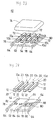
- Fig. 39 is a perspective view of a conventional piezoelectric resonator.
- a piezoelectric resonator 1 includes a piezoelectric substrate 2 having, for example, a rectangular plate shape viewed from the top.
- the piezoelectric substrate 2 is polarized in the thickness direction.
- electrodes 3 are formed on both surfaces of the piezoelectric substrate 2.
- a signal is input between the electrodes 3, an electrical field is applied to the piezoelectric substrate 2 in the thickness direction and the piezoelectric substrate 2 vibrates in the longitudinal direction.
- Fig. 40 there is shown a piezoelectric resonator 1 in which electrodes 3 are formed on both surfaces of a piezoelectric substrate 2 having a square plate shape viewed from the top.
- the piezoelectric substrate 2 of the piezoelectric resonator 1 is polarized in the thickness direction.
- a signal is input between the electrodes 3 in the piezoelectric resonator 1, an electrical field is applied to the piezoelectric substrate 2 in the thickness direction and the piezoelectric substrate 2 vibrates in square-type vibration mode (in the plane direction).
- These piezoelectric resonators are of an unstiffened type, in which the vibration direction differs from the direction of polarization and the electrical field.
- the electromechanical coupling coefficient of such an unstiffened piezoelectric resonator is lower than that of a stiffened piezoelectric resonator, in which the vibration direction, the direction of polarization, and the direction in which an electrical field is applied are the same.
- An unstiffened piezoelectric resonator has a relatively small frequency difference ⁇ F between the resonant frequency and the antiresonant frequency. This leads to a drawback in which a frequency-band width in use is narrow when an unstiffened frequency resonator is used as an oscillator or a filter. Therefore, the degree of freedom in characteristics design is low in such a piezoelectric resonator and electronic components using the same.
- the piezoelectric resonator shown in Fig. 39 uses the first-order resonance in the longitudinal mode. It also generates due to its structure large spurious resonances in odd-number-order harmonic modes, such as the third-order and fifth-order modes, and in width mode. To suppress these spurious resonances, some measures are considered, such as polishing, increasing mass, and changing the shape of the electrode. These measures increase manufacturing cost.
- the piezoelectric substrate since when viewed from the top the piezoelectric substrate has a rectangular plate shape, the substrate cannot be thinner due to restrictions in strength. Therefore, the distance between the electrodes cannot be reduced and a capacitance between terminals cannot be made large. This is extremely inconvenient for achieving impedance matching with an external circuit.
- the electrodes are only partially made, the difference ⁇ F between the resonant frequency and the antiresonant frequency as well as the capacitance is reduced.
- the resonators connected in parallel are accordingly required to have small ⁇ F. As a result, the piezoelectricity of the piezoelectric substrate is not effectively used, and the transmission band width of the filter cannot be increased.
- a piezoelectric resonator of the above mentioned kind which is characterized in that an inactive section, which is not polarized and/or not energized by an electric field, constitutes the other part of said base member.
- the inactive section is provided at both ends of said active section, and said active section occupies 50% of said base member or more in longitudinal direction. at least one pair of internal electrodes is disposed in said active section such
- the above mentioned piezoelectric resonaror may be a piezoelectric resonaror which is characterized in that the internal electrodes are perpendicular to the longitudinal direction of said base member and are connected to said pair of external electrodes respectively, said active section is polarized in the longitudinal direction of said base member, and said base member excites a longitudinal mode basic vibration when an electric field is applied to the longitudinal direction of said base member via said internal electrodes.
- the piezoelectric resonator may further include a support member at a center of said base member in the longitudinal direction.
- an electronic component for use with the above mentioned piezoelectric resonators which is characterized in that said support member is provided on a insulating substrate, and a pattern electrode is provided on said insulating substrate and connected to said external electrodes of said piezoelectric resonator.
- a cap may be disposed on the insulating substrate so as to cover the base member.
- the electronic component may be a ladder filter in which a plurality of said pattern electrodes are provided on said insulating substrate and connected to said external electrodes of a plurality of said piezoelectric resonators such that said piezoelectric resonators are connected to each other in a ladder shape.
- a cap may also be disposed on the insulating substrate so as to cover the base member.
- This invention also provides an electronic component for use with the above piezoelectric resonator, which is characterized in that a mounting member is provided with said support member, and said piezoelectric resonator is fixed in a case by said mounting member.
- the forgoing object is achieved in still another aspect of the present invention through the provision of a manufacturing method of the above mentioned electronic components, comprising the steps of: 1)preparing a laminated member in which a plurality of piezoelectric layers and a plurality of internal electrodes are laminated, 2)forming an external electrode on a surface of said laminated member at which ends of said internal electrodes are exposed, 3)cutting said laminated member perpendicular to said surface of said laminated member.
- the laminated member may be prepared in such a way that said internal electrodes are alternately exposed at opposite sides of said piezoelectric layers, one pair of polarizing electrodes are formed on said opposite sides of said piezoelectric layers and electrically connected to every other said internal electrodes respectively, said piezoelectric layers are polarized by applying a DC voltage via said polarizing electrodes and said internal electrodes, and said piezoelectric member and said internal electrodes are cut perpendicularly to a laminated direction thereof.
- the frequency difference ⁇ F is adjusted by adjusting the inactive section, the frequency-band width of the piezoelectric resonator can be changed.
- the piezoelectric resonator according to the present invention is of a stiffened type, and has an active section in which the vibration direction, the direction of polarization, and the direction in which an electrical field is applied are the same. Therefore, as compared with an unstiffened piezoelectric resonator, in which the vibration direction differs from the direction of polarization and electrical field, the stiffened piezoelectric resonator has a larger electromechanical coupling coefficient and a larger frequency difference ⁇ F between the resonant frequency and the antiresonant frequency. In addition, vibrations in modes such as the width and thickness modes, which are different from the basic vibration, are unlikely to occur in a stiffened piezoelectric resonator. Furthermore, the capacitance can be adjusted by changing the number of electrodes which are used for applying an electric field to the active section, the distances thereof, and the size thereof. The frequency difference ⁇ F can be adjusted by trimming an inactive section provided or by adding mass to the section.
- the piezoelectric resonator When electronic components such as an oscillator, a discriminator, and a filter are made using the piezoelectric resonator, the piezoelectric resonator is mounted on an insulating substrate on which pattern electrodes are formed and is covered by a cap to form chip-type (surface mount) electronic components.
- the frequency difference ⁇ F between the resonant frequency and the antiresonant frequency is large as compared with a conventional piezoelectric resonator, and thus a wide-frequency-band resonator is obtained
- a chip-type electronic component can be made using the piezoelectric resonator, it is easy to mount the component on a circuit board. It is also easy to achieve impedance matching between such an electronic component and an external circuit by adjusting the capacitance of the piezoelectric resonator.
- attenuation in the filter can be adjusted by changing the ratio of the capacitance of the piezoelectric resonator connected in series to that of the piezoelectric resonator connected in parallel.
- Fig. 1 is a perspective view of a piezoelectric resonator according to the present invention.
- Fig. 2 is a view showing the structure of the piezoelectric resonator shown in Fig. 1.
- Fig. 3 is a perspective view indicating how ceramic green sheets are laminated in order to produce the piezoelectric resonator shown in Fig. 1.
- Fig. 4 is a view showing a laminated block formed by the ceramic green sheets shown in Fig. 3.
- Fig. 5 is a view showing portions where the laminated block shown in Fig. 4 is cut.
- Fig. 6 is a view showing a plate-shaped block made by cutting the laminated block shown in Fig. 5.
- Fig. 7 is a view showing the condition in which a resin insulating material is applied to the plate-shaped block shown in Fig. 6 and external electrodes are formed.
- Fig. 8 is a perspective view of an unstiffened piezoelectric resonator which vibrates in the longitudinal direction, which is shown for comparison.
- Fig. 9 is a perspective view of a stiffened piezoelectric resonator which vibrates in the longitudinal direction.
- Fig. 10 is a perspective view of an unstiffened piezoelectric resonator which vibrates in the plane direction (square-type vibration), which is shown for comparison.
- Fig. 11 is a chart showing the relationship between the frequency and the impedance of the piezoelectric resonator according to the present invention.
- Fig. 12 is a chart showing the relationship between the frequency and the impedance of a conventional piezoelectric resonator.
- Fig. 13 is a view of a piezoelectric resonator in which the distribution of an active section and inactive sections is changed in a base member.
- Fig. 14 is a chart indicating the relationship between the distribution of an active section and capacitance, and ⁇ F/Fa.
- Fig. 15 is a chart showing the relationship between an active-section ratio and ⁇ F.
- Fig. 16 is a view showing a modified piezoelectric resonator according to the present invention.
- Fig. 17 is a view showing another modified piezoelectric resonator according to the present invention.
- Fig. 18 is a view showing still another piezoelectric resonator according to the present invention.
- Fig. 19 is a view indicating the gap between the end of an internal electrode and a side face of a base member in the piezoelectric resonator shown in Fig. 18.
- Fig. 20 is a chart indicating the relationships between the capacitance and ⁇ F, and the gap between an internal electrode and a side face of the base member.
- Fig. 21 is a plan showing modified piezoelectric layers of the piezoelectric resonator shown in Fig. 18.
- Fig. 22 is a view showing a piezoelectric resonator having the piezoelectric layers shown in Fig. 21.
- Fig. 23 is a view showing a modified inactive section of a piezoelectric resonator.
- Fig. 24 is a view showing another modified inactive section of a piezoelectric resonator.
- Fig. 25 is a view showing an electrode formed at an end of a base member.
- Fig. 26 is a perspective view of an electronic component using the above-described piezoelectric resonator.
- Fig. 27 is a perspective view of an insulating substrate used in the electronic component shown in Fig. 26.
- Fig. 28 is an exploded perspective view of the electronic component shown in Fig. 26.
- Fig. 29 is a view indicating another method for mounting the piezoelectric resonator to the insulating substrate.
- Fig. 30 is a side view showing the method for mounting the piezoelectric resonator, shown in Fig. 29.
- Fig. 31 is a view indicating still another method for mounting the piezoelectric resonator to the insulating substrate.
- Fig. 32 is a side view showing the method for mounting the piezoelectric resonator, shown in Fig. 31.
- Fig. 33 is an exploded perspective view of a ladder filter using the piezoelectric resonators according to the present invention.
- Fig. 34 is a perspective view of an insulating substrate and the piezoelectric resonators in the ladder filter shown in Fig. 33.
- Fig. 35 is an equivalent circuit diagram of the ladder filter shown in Fig. 33.
- Fig. 36 is a view showing an electronic component in which a piezoelectric resonator having different-shaped external electrodes is mounted on an insulating substrate.
- Fig. 37 is an exploded perspective view of a two-terminal electronic component.
- Fig. 38 is a chart indicating the relationship between Cf and ⁇ F/Fa, and other parameters.
- Fig. 39 is a view of a conventional unstiffened piezoelectric resonator.
- Fig. 40 is a view of another conventional unstiffened piezoelectric resonator.
- Fig. 1 is a perspective view of a piezoelectric resonator according to an embodiment of the present invention.
- Fig. 2 shows the internal structure of the piezoelectric resonator.
- the piezoelectric resonator 10 includes a base member 12 having, for example, a cubic shape.
- the base member 12 is made from, for example, a piezoelectric, ceramic material.
- a plurality of electrodes 14 is formed in the base member 12 such that the surfaces of the electrodes 14 are perpendicular to the longitudinal direction of the base member 12.
- the base member 12 is polarized in the longitudinal direction such that the directions of polarization oppose each other at both sides of one electrode 14.
- a plurality of insulating films 16 and 18 is formed, respectively.
- the insulating film 16 covers the exposed section of every other electrode 14.
- the insulating film 18 covers the exposed section of every other electrode 14 not covered by the insulating film 16 on the above-described side face.
- some electrodes 14 disposed near both ends of the base member 12 are successively covered by the insulating film 16 and 18.
- three consecutive electrodes 14 from each end of the base member 12 are covered by the insulating film 16, and two consecutive electrodes 14 from each end of the base member 12 are covered by the insulating film 18.
- the side faces of the base member 12 on which the insulating film 16 and 18 is formed serve as connection sections to external electrodes, which will be described later.
- connection sections namely, the side faces of the base member 12 on which the insulating films 16 and 18 are formed.
- the electrode 20 connects to electrodes 14 which are not covered by the insulating film 16, and the electrode 22 connects to electrodes 14 which are not covered by the insulating film 18.
- two adjacent electrodes 14 are connected to the electrodes 20 and 22, respectively, except that some of the electrodes 14 disposed at both ends of the base member 12 are not connected to the external electrodes 20 and 22.
- the piezoelectric resonator 10 uses the external electrodes 20 and 22 as input and output electrodes.
- the base member 12 is piezoelectrically active because an electric field is applied between adjacent electrodes 14.
- the base member 12 is piezoelectrically inactive at both ends because an electric field is not applied between adjacent electrodes 14 since the electrodes 14 are insulated. Therefore, an active section 24 for input signals is formed at the center of the base member 12 as shown by hatching in Fig. 2.
- Inactive sections 26 for input signals are also formed at both ends of the base member 12.
- green sheets 30 made from piezoelectric ceramic are first prepared as shown in Fig. 3.
- electrically conductive paste including, for example, silver, palladium, and an organic binder, is applied to form an electrically conductive paste layer 32 over almost the entire area of each green sheet 30 excluding an end portion.
- a plurality of green sheets 30 is laminated such that the end portions where the electrically conductive paste layers 32 are not formed on the green sheets are placed alternately in opposite directions.
- the laminated member with electrically conductive paste applied to opposite side faces is baked to form a laminated block 34 shown in Fig. 4.
- the laminated block 34 has a plurality of internal electrodes 36, which have been made by baking the electrically conductive layers 32. External electrodes 38 and 40 formed on opposite side faces are connected to every other internal electrode 36, respectively, since the internal electrodes 36 are alternately exposed on opposite side faces of the laminated block 34.
- a DC voltage is applied to the external electrodes 38 and 40, the laminated block 34 is polarized.
- a high DC electric field is applied between adjacent internal electrodes 36 alternately in opposite directions. Therefore, the laminated block 34 is polarized in the opposite directions at both sides of the internal electrodes 36 as shown by arrows in Fig. 4.
- the laminated block 34 is surface-ground to the desired thickness since the antiresonant frequency of the resonator is determined by the thickness of the laminated block 34.
- the laminated block 34 is cut by a dicing machine along dotted lines shown in Fig. 5 such that the cutting planes are perpendicular to the plurality of internal electrodes 36.
- a plate-shaped block 42 shown in Fig. 6 is obtained.
- a resin insulating material 44 is applied to both surfaces of the plate-shaped block 42 as shown in Fig. 7 such that the material 44 is applied to every other internal electrode 36 on one surface and every other internal electrode 36 to which the material 44 is not applied, on the other surface.
- the resin insulating material 44 is applied to the internal electrodes 36 collectively.
- External electrodes 48 are formed on the plate-shaped block 42. Then, the resultant block is cut perpendicularly to the internal electrodes 36 to form the piezoelectric resonator 10 shown in Fig. 1.
- the piezoelectric resonator 10 vibrates in the longitudinal direction in basic mode, in which the center of the base member 12 is served as a node.
- the piezoelectric resonator 10 In the piezoelectric resonator 10, the polarization direction of the active section 24, the applied electric field direction due to a signal, and the direction of vibration in the active section 24 are all the same.
- the piezoelectric resonator 10 is of stiffened type.
- the stiffened piezoelectric resonator 10 has a larger electromagnetic coupling coefficient than an unstiffened piezoelectric resonator, in which the direction of vibration differs from the direction of polarization and electric field. Therefore, the piezoelectric resonator 10 has a larger frequency difference ⁇ F between the resonant frequency and the antiresonant frequency than the conventional piezoelectric resonator. This means that the piezoelectric resonator 10 obtains wide-frequency-band characteristics.
- piezoelectric resonators shown in Figs. 8, 9, and 10 were made.
- the piezoelectric resonator shown in Fig. 8 was made by forming electrodes on both surfaces in the thickness direction of a piezoelectric substrate measuring 4.0 mm by 1.0 mm by 0.38 mm. This piezoelectric resonator was polarized in the thickness direction and vibrated in the longitudinal direction when a signal was applied to the electrodes.
- the piezoelectric resonator shown in Fig. 9 had the same dimensions as the piezoelectric resonator shown in Fig. 8. Electrodes were formed on both surfaces in the longitudinal direction of a piezoelectric substrate.
- the piezoelectric resonator was polarized in the longitudinal direction and vibrated in the longitudinal direction when a signal was applied to the electrodes.
- the piezoelectric resonator shown in Fig. 10 was made by forming electrodes on both surfaces in the thickness direction of a piezoelectric substrate measuring 4.7 mm by 4.7 mm by 0.38 mm. This piezoelectric resonator was polarized in the thickness direction and vibrated in the plane direction when a signal was applied to the electrodes.
- the piezoelectric resonators shown in Figs. 8 and 10 were of unstiffened type and the piezoelectric resonator shown in Fig. 9 was of stiffened type.
- Table 1 indicates the measured results of the piezoelectric resonator shown in Fig. 8.
- Table 2 indicates the measured results of the piezoelectric resonator shown in Fig. 9.
- Table 3 indicates the measured results of the piezoelectric resonator shown in Fig. 10.
- a stiffened piezoelectric resonator has a larger electromagnetic coupling coefficient K than an unstiffened piezoelectric resonator, and therefore has a larger frequency difference ⁇ F between the resonant frequency and the antiresonant frequency.
- the largest spurious vibration in a stiffened piezoelectric resonator is of longitudinal triple-wave type and the electromagnetic coupling coefficient K is 12.2% during vibration.
- the electromagnetic coupling coefficient K is 4.0%.
- the electromagnetic coupling coefficient K during width-mode vibration is 25.2% in an unstiffened longitudinal-vibration piezoelectric resonator.
- the electromagnetic coupling coefficient K is as large as 23.3% during thickness-mode vibration. Therefore, it is understood that a stiffened piezoelectric resonator has smaller spurious vibrations than an unstiffened piezoelectric resonator.
- the inactive section 26 is formed at both ends of the base member 12.
- the inactive section is changed to adjust the resonant frequency and the difference ⁇ F between the resonant frequency and the antiresonant frequency. In other words, by grinding the end faces in the longitudinal direction of the base member 12 or by adding mass, the band width of the piezoelectric resonator 10 can be adjusted.
- the capacitance of the resonator can be adjusted by, for example, changing the number of layers in the active section 24.
- the active section 24 piezoelectric layers and electrodes 14 are alternately stacked and electrically connected in parallel.
- Capacitance of resonator ⁇ (the number of layers in active section/thickness of a layer) ⁇ (the number of layers in active section) 2
- the capacitance of the resonator is proportional to the square of the number of layers in the active section 24. Therefore, the number of layers in the active section 24 is changed to adjust the capacitance of the piezoelectric resonator 10. This means that the piezoelectric resonator 10 has a large degree of freedom in capacitance design. Therefore, it is easy to achieve impedance matching with an external circuit when the piezoelectric resonator 10 is mounted on a circuit board.
- Electrically conductive paste including, for example, silver, palladium, and an organic binder, was applied to one surface of each green sheet 30 made from piezoelectric ceramic.
- a plurality of such green sheets were stacked alternately and baked integrally at 1200 °C to form a laminated block 34 measuring 20 mm by 30 mm by 3.9 mm.
- External electrodes 38 and 40 were formed by sputtering.
- a high DC electric field was applied between adjacent internal electrodes 36 to polarize the laminated block such that the directions of polarization in adjacent piezoelectric layers were alternately opposed.
- the thickness of the laminated block 34 was changed.
- the laminated block 34 was cut to form a plate-shaped block 42 measuring 1.5 mm by 30 mm by 3.8 mm.
- Every other electrodes 36 exposed at the side faces of the plate-shaped block 42 were covered by a resin insulating material 44 and a silver electrode was formed on it by sputtering.
- the resultant block was cut by a dicing machine to obtain a piezoelectric resonator 10 measuring 1.5 mm by 1.5 mm by 3.8 mm.
- the piezoelectric resonator 10 had nineteen electrodes 14 in the base member 12, the electrodes 14 being disposed at an almost equal interval of 0.19 mm. Insulting films 16 and 18 were formed so as to avoid applying an electric field to three piezoelectric layers disposed at both ends of the base member 12. An active section 24 included 14 piezoelectric layers disposed at the center of the base member 12, and an inactive section 26 had three piezoelectric layers at both ends.
- the piezoelectric resonator 10 had a capacitance of 830 pF and the frequency characteristics shown in Fig. 11. For comparison, the frequency characteristics of a square-type vibration piezoelectric resonator is shown in Fig. 12. It is found from Figs. 11 and 12 that the piezoelectric resonator 10 according to the present invention has much less spurious vibration than the square-shaped piezoelectric resonator.
- Inactive sections 26 can be formed, for example as shown in Fig. 13, at both ends and the center of the base member 12.
- the finite element method was used to calculate changes in capacitance Cf and frequency difference ⁇ F in the piezoelectric resonator in a case in which the positions where active sections were formed change, where "a" indicates the distance between the center and an end of the piezoelectric resonator 10, "b” indicates the distance between the center and the center of gravity of an active section 24, "c” indicates the length of the active sections 24, W indicates the width of the base member 12, and T indicates the thickness of the base member 12.
- the frequency difference ⁇ F can be changed in the piezoelectric resonator 10 by changing the ratio of the active sections 24 to the inactive sections 26.
- a changing active-section ratio which is a ratio of the length of the active section 24 to that of the base member 12 in the piezoelectric resonator 10 shown in Figs. 1 and 2, the resonant frequency Fr, the antiresonant frequency Fa, the frequency difference ⁇ F, and its rate of change were measured and are indicated in Table 4 and Fig. 15.
- Fig. 15 shows the relationship between the active-section ratio and change in ⁇ F under the condition in which ⁇ F is set to 100% when the active-section ratio is 100%, namely when an inactive section does not exist. It is found from Fig. 15 that ⁇ F is large at an active-section ratio of 65% to 85% with the peak ⁇ F being obtained at an active-section ratio of 75%. The peak value is larger by about 10% than the ⁇ F obtained when the active-section ratio is 100%, in other words, when an inactive section does not exist. The same ⁇ F is obtained at active-section ratios of 50% and 100%. Therefore, to obtain a piezoelectric resonator having a large ⁇ F, it is necessary to set the active-section ratio to 50%.
- the capacitance In the piezoelectric resonator 10, when 14 piezoelectric layers constituted the active section 24 among 20 layers, the capacitance was 830 pF. In contrast, when the active-section ratio was set to 100%, which means that only one piezoelectric layer was used, in other words, when electrodes were formed at both end faces of the base member 12, with the same material and the same dimensions, the capacitance was 3.0 pF. When all of the 24 piezoelectric layers constituted the active section 24, the capacitance was 1185.6 pF. By changing the number of layers in the piezoelectric resonator 10, the capacitance can be changed within a range of about 400-times difference between the minimum and maximum. Therefore, by changing the lamination structure of the piezoelectric resonator 10, the capacitance can be selected from a wide range which provides a large degree of freedom in capacitance design.
- insulating film 16 and 18 having windows 50 may be provided such that every other electrode 14 is exposed as shown in Fig. 16.
- the external electrodes 20 and 22 are formed on the insulating film 16 and 18, and the electrodes 14 connect to the two external electrodes 20 and 22 alternately.
- Two external electrodes 20 and 22 may be formed on one side face of the base member 12 as shown in Fig. 17.
- Insulating films 16 and 18 are formed on one side face of the base member 12 in a two-row manner and two rows of connection sections are formed. These two rows of insulating film 16 and 18 are formed respectively on every other electrode 14. On these two rows of insulating film 16 and 18, two rows of external electrodes 20 and 22 are formed, respectively.
- the piezoelectric resonators having these modifications can achieve the same advantages as the above-described piezoelectric resonator.
- Internal electrodes 14 may reach the opposite side faces of the base member 12 alternately as shown in Fig. 18. On the opposite side faces of the base member 12, it is necessary to form external electrodes 20 and 22. In such a piezoelectric resonator 10, since the electrodes 14 formed inside are exposed alternately, the internal electrodes 14 are connected to the external electrodes 20 and 22 by forming the external electrodes 20 and 22 on the side faces of the base member 12. Therefore, there is no need to form insulating film on the side faces of the base member 12.
- An electrode 14 is not formed on the entire area of a cross section of the base member 12 in this piezoelectric resonator 10. Therefore, the opposing area of adjacent electrodes 14 is smaller than that of adjacent electrodes 14 formed in the entire cross section. By the opposing area, the capacitance and ⁇ F of the piezoelectric resonator 10 can be adjusted.
- the antiresonant frequency Fa, capacitance Cf, and ⁇ F of a piezoelectric resonator having a base member 12 which is 3.74 mm long, 0.8 mm wide, 1.0 mm thick, and having an active section 24 3.6 mm long, inactive sections 26 disposed at both ends 0.07 mm long and 20 piezoelectric layers each 0.18 mm thick were calculated.
- the results are shown in Table 5 and Fig. 20. It is found from Table 5 and Fig. 20 that Cf and ⁇ F become smaller as the gap G increases, in other words, as the opposite area of the electrodes 14 becomes smaller.
- Electrodes 14 may be formed such that they reach different end faces on the same side of piezoelectric layers as shown in Fig. 21 in a piezoelectric resonator 10 which is a modified example of the above-described piezoelectric resonator 10.
- a piezoelectric resonator 10 which is a modified example of the above-described piezoelectric resonator 10.
- two rows of electrodes 14 are exposed on one side face of the base member 12 as shown in Fig. 22. Therefore, by forming external electrodes 20 and 22 at portions where the electrodes 14 are exposed, the electrodes 14 are alternately connected to the external electrodes 20 and 22.
- each electrode 14 is formed over the entire cross section of the base member 12 as shown in Fig. 2
- the electromagnetic coupling coefficient of the resonator is large and thus ⁇ F is large.
- the capacitance of the piezoelectric resonator 10 is also large.
- resonators having different cross sections, different areas, and different capacitances are obtained from the same piezoelectric, ceramic, laminated block.
- Resonators having various capacitances and various ⁇ F can be obtained according to which electrode end section has insulating film. As described above, many types of piezoelectric resonators can be obtained from the same laminated block.
- An inactive section 26 may be formed such that an electric field is not applied by not forming electrodes 14 at an end of the base member 12 as shown in Fig. 23.
- the end of the base member 12 may be polarized or may not be polarized. As shown in Fig. 24, only the end of the base member 12 may not be polarized. In this case, even if an electric field is applied between the electrodes 14, a portion not polarized is piezoelectrically inactive. In other words, only when a piezoelectric layer is polarized and an electric field is applied, the layer becomes piezoelectrically active, otherwise it is inactive. In this configuration, the capacitor is formed in the inactive section, and the capacitance can be increased.
- a small electrode 52 may be formed on an end face of the base member 12 as shown in Fig. 25 in order to adjust the frequency or to connect to an external circuit.
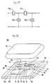
- Fig. 26 is a perspective view of an electronic component 60.
- the electronic component 60 includes an insulating substrate 62. At opposing end portions of the insulating substrate 62, two indentations 64 are formed, respectively. On one surface of the insulating substrate 62, two pattern electrodes 66 and 68 are formed as shown in Fig. 27.
- One pattern electrode 66 is formed between opposing indentations and extends in an L-shaped manner from a point near one end toward the center of the insulating substrate 62.
- the other pattern electrode 68 is formed between opposing indentations 64 and extends straight from a point near the other end toward the center of the insulating substrate 62.
- the pattern electrodes 66 and 68 are formed such that they are routed in a roundabout fashion from the ends of the insulating substrate 62 to the opposite ends.
- a protrusion 70 (served as a support member) is formed with electrically conductive adhesive.
- the above-described piezoelectric resonator 10 is mounted on the protrusion 70 such that the center of the base member 12 is disposed on the protrusion 70.
- An external electrode 22 of the piezoelectric resonator 10 is, for example, connected to the protrusion 70.
- the other external electrode 20 is connected to a pattern electrode 68 with electrically conductive wire 72.
- the electrically conductive wire 72 is connected to the center of the external electrode 20 of the piezoelectric resonator 10.
- a metal cap 74 is placed on the insulating substrate 62 to complete the electronic component 60.
- insulating resin is applied to the insulating substrate 62 and the pattern electrodes 66 and 68 in advance.
- the electronic component 60 uses the pattern electrodes 66 and 68, which are formed such that they are routed to the rear surface from ends of the insulating substrate 62, as input and output terminals for connecting to external circuits.
- the center of the piezoelectric resonator 10 is connected to the protrusion 70 in this electronic component 60, the ends of the piezoelectric resonator 10 are disposed separately from the insulating substrate 62 so vibration is not prevented. Excited longitudinal vibration is not weakened because the center of the piezoelectric resonator, which serves as a node, is secured to the protrusion 70 and is connected to the electrically conductive wire 72.
- the electronic component 60 is mounted on a circuit board together with IC chips and other components to form an oscillator and a discriminator. Since the electronic component 60 is sealed and protected by the metal cap 74, it can be used as a chip-type (surface mount) component which can be mounted by reflow soldering.
- the electronic component 60 When the electronic component 60 is used for a discriminator, a wide peak-separation range is provided due to a large ⁇ F of the resonator. In addition, since the resonator provides a wide capacitance range, it is easy to achieve impedance matching with an external circuit.
- the piezoelectric resonator 10 may be mounted on the insulating substrate 62 so that two protrusions 70 made from an electrically conductive material such as electrically conductive adhesive are formed on both pattern electrodes 66 and 68, and the external electrodes 20 and 22 of the piezoelectric resonator 10 are connected to the two protrusions 70, as shown in Figs. 29 and 30.
- the piezoelectric resonator 10 may also be mounted on the insulating substrate 62 in a way shown in Figs. 31 and 32 in which two protrusions 70 made from an insulating material such as insulating adhesive are formed on the insulating substrate 62 and the external electrodes 20 and 22 are connected to the pattern electrodes 66 and 68 with electrically conductive wire 72.
- a ladder filter can be made using a plurality of the piezoelectric resonators 10. As shown in Figs. 33 and 34, three pattern electrodes 76, 78, and 80 are formed on an insulating substrate 62 in this electronic component 60. Protrusions 82 and 86 are formed with electrically conductive adhesive on both-end pattern electrodes 76 and 80. On the center pattern electrode 78, two protrusions 84 and 88 are formed with electrically conductive adhesive.
- One external electrode 22 for each of piezoelectric resonators 10a, 10b, 10c, and 10d is mounted to each of the protrusions 82, 84, 86, and 88, respectively.
- the other external electrodes 20 for piezoelectric resonators 10a, 10b, and 10c are connected to each other with electrically conductive wire 72.
- the other external electrode 20 of a piezoelectric resonator 10d is connected to the pattern electrode 80 with electrically conductive wire 72.
- a metal cap 74 is placed on the insulating substrate 62.
- the electronic component 60 is used as a ladder filter having a ladder-shaped circuit shown in Fig. 35.
- Two piezoelectric resonators 10a and 10c serve as series resonators and the other two piezoelectric resonator 10c and 10d serve as parallel resonators.
- the parallel piezoelectric resonators 10b and 10d are designed to have substantially larger capacitances than the series piezoelectric resonators 10a and 10c.
- Attenuation in the ladder filter is determined by the capacitance ratio between the series resonators and the parallel resonators.
- the capacitance can be adjusted by changing the number of laminated layers used in the piezoelectric resonators 10a to 10d. Therefore, a ladder filter having a larger attenuation with fewer resonators is implemented by changing the capacitances of the piezoelectric resonators, as compared with a case where the conventional unstiffened piezoelectric resonators are used. Since the piezoelectric resonators 10a to 10d have a larger ⁇ F than the conventional piezoelectric resonator, a wider transmission frequency band is implemented as compared with the conventional piezoelectric resonator.
- Fig. 36 shows such an electronic component 60 in which two electrodes 14 are formed inside the base member 12 of the piezoelectric resonator 10.
- the inactive sections 26 occupy 25% (12.5% each) of the base member 12 in length.
- External electrodes 20 and 22 are formed such that they extend from the internal electrodes 14 to the centers of side faces of the base member 12, respectively.
- the shapes of the external electrodes 20 and 22 are adjusted according to the number of the internal electrodes 14 and their forming conditions.
- a two-terminal electronic component 60 such as a ceramic resonator and a ceramic discriminator can be produced with a piezoelectric resonator 10 as shown in Fig. 37.
- Two terminals 90 made from an electrically conductive material are prepared to produce such a two-terminal component 60. These terminals 90 are formed such that they extend from hoops 92. Practically, a plurality of terminals 90 are formed on each hoop 92 in line.
- a terminal 90 is provided with a fold section 94 at the intermediate portion and an H-shaped support member 96 at the end. The support member 96 is bent and is provided with a protruded mounting member 98 at the center.
- the two terminals 90 are disposed such that their mounting members 98 oppose each other.
- the piezoelectric resonator 10 is supported between the mounting members 98.
- the mounting members 98 abut against the external electrodes 20 and 22 at the center of the piezoelectric resonator in the longitudinal direction. Since the terminals 90 have fold sections 94, which serve as spring elements, the piezoelectric resonator 10 is spring-supported by the terminals 90.
- a case 100 having an opening at one end is placed on the piezoelectric resonator 10. The opening of the case 100 is closed with paper and then resin-sealed.
- the terminals 90 are cut from the hoops 92 to complete the electronic component 60.
- the electronic component 60 having a shape other than a chip-shape can thus be made.
- the resonator Since the present invention employs a stiffened piezoelectric resonator, the resonator has a larger ⁇ F and a wider frequency band than the conventional unstiffened piezoelectric resonator. In addition, the stiffened piezoelectric resonator has small spurious vibrations. Since the base member 12 has a laminated structure, the capacitance can be set to any desired value and it is easy to achieve impedance matching with an external circuit. Furthermore, by adjusting the sizes and positions of the active section and the inactive sections, ⁇ F can be changed. Since the electronic component 60 according to the present invention has a simple structure, it can be produced at a low cost while exhibiting the above-described features of the piezoelectric resonator 10.
- the piezoelectric resonator 10 since the piezoelectric resonator 10 according to the present invention includes more parameters which can be designed than the conventional piezoelectric resonator, various characteristics can be implemented. The relationships between these parameters, ⁇ F/Fa and capacitance Cf are indicated in Fig. 38. It is understood from Fig. 38 that these parameters extend the degree of freedom in designing the characteristics of the piezoelectric resonator 10.
Landscapes
- Physics & Mathematics (AREA)
- Acoustics & Sound (AREA)
- Chemical & Material Sciences (AREA)
- Crystallography & Structural Chemistry (AREA)
- Piezo-Electric Or Mechanical Vibrators, Or Delay Or Filter Circuits (AREA)
Applications Claiming Priority (3)
| Application Number | Priority Date | Filing Date | Title |
|---|---|---|---|
| JP11047596 | 1996-04-05 | ||
| JP11047596A JP3271517B2 (ja) | 1996-04-05 | 1996-04-05 | 圧電共振子およびそれを用いた電子部品 |
| JP110475/96 | 1996-04-05 |
Publications (3)
| Publication Number | Publication Date |
|---|---|
| EP0800269A2 true EP0800269A2 (fr) | 1997-10-08 |
| EP0800269A3 EP0800269A3 (fr) | 1998-02-04 |
| EP0800269B1 EP0800269B1 (fr) | 2003-12-10 |
Family
ID=14536662
Family Applications (1)
| Application Number | Title | Priority Date | Filing Date |
|---|---|---|---|
| EP97105313A Expired - Lifetime EP0800269B1 (fr) | 1996-04-05 | 1997-03-27 | Résonateur piézoélectrique et composant électronique en faisant usage |
Country Status (6)
| Country | Link |
|---|---|
| US (1) | US5925970A (fr) |
| EP (1) | EP0800269B1 (fr) |
| JP (1) | JP3271517B2 (fr) |
| CN (1) | CN1085908C (fr) |
| DE (1) | DE69726636T2 (fr) |
| NO (1) | NO971560L (fr) |
Cited By (9)
| Publication number | Priority date | Publication date | Assignee | Title |
|---|---|---|---|---|
| EP0802629A2 (fr) * | 1996-04-18 | 1997-10-22 | Murata Manufacturing Co., Ltd. | Composant électronique et filtre en échelle |
| EP0818881A2 (fr) * | 1996-07-10 | 1998-01-14 | Murata Manufacturing Co., Ltd. | Résonateur piézoélectrique et composant électronique en faisant usage |
| EP0820144A2 (fr) * | 1996-07-18 | 1998-01-21 | Murata Manufacturing Co., Ltd. | Résonateur piézoélectrique et composant électrique en faisant usage |
| EP0821482A2 (fr) * | 1996-07-26 | 1998-01-28 | Murata Manufacturing Co., Ltd. | Résonateur piézoélectrique et composant électrique utilisant ce résonateur |
| EP0823781A2 (fr) * | 1996-08-05 | 1998-02-11 | Murata Manufacturing Co., Ltd. | Résonateur piézoélectrique, son procédé de fabrication et composant électronique utilisant ce résonateur |
| EP0827273A2 (fr) * | 1996-08-27 | 1998-03-04 | Murata Manufacturing Co., Ltd. | Résonateur piézoélectrique et composant électronique utilisant ce résonateur |
| EP0829957A2 (fr) * | 1996-09-12 | 1998-03-18 | Murata Manufacturing Co., Ltd. | Résonateur piézoélectrique et composant électronique en faisant usage |
| EP0845859A2 (fr) * | 1996-11-28 | 1998-06-03 | Murata Manufacturing Co., Ltd. | Résonateur piézoélectrique et composant électronique utilisant ce résonateur |
| EP1006596A2 (fr) * | 1998-12-01 | 2000-06-07 | Murata Manufacturing Co., Ltd. | Elément multicouche piézo-électrique |
Families Citing this family (10)
| Publication number | Priority date | Publication date | Assignee | Title |
|---|---|---|---|---|
| JP3368214B2 (ja) * | 1997-10-01 | 2003-01-20 | 株式会社村田製作所 | ラダーフィルタおよび通信機器 |
| JP3262076B2 (ja) * | 1997-10-03 | 2002-03-04 | 株式会社村田製作所 | 圧電共振子、圧電共振子の周波数調整方法および通信機器 |
| JPH11341838A (ja) * | 1998-05-20 | 1999-12-10 | Tokin Ceramics Corp | 積層型圧電アクチュエータ |
| JP3669431B2 (ja) * | 2001-08-20 | 2005-07-06 | 株式会社村田製作所 | 圧電型電気音響変換器 |
| US6800986B2 (en) * | 2002-01-23 | 2004-10-05 | Tdk Corporation | Piezoelectric sensor |
| US6811385B2 (en) * | 2002-10-31 | 2004-11-02 | Hewlett-Packard Development Company, L.P. | Acoustic micro-pump |
| US7235916B2 (en) * | 2004-06-03 | 2007-06-26 | Zippy Technology Corp. | Piezoelectric blades anchoring structure |
| US7728716B2 (en) * | 2007-08-01 | 2010-06-01 | China Steel Corporation | Piezoelectric buzzer |
| DE102012215774A1 (de) * | 2012-09-06 | 2014-03-06 | Robert Bosch Gmbh | Piezoelektrischer Aktor |
| CH713460A2 (de) * | 2017-02-15 | 2018-08-15 | Digi Sens Ag | Schwingsaitensensor und Schwingsaite für einen Schwingsaitensensor. |
Citations (3)
| Publication number | Priority date | Publication date | Assignee | Title |
|---|---|---|---|---|
| GB2087184A (en) * | 1980-10-22 | 1982-05-19 | Ngk Spark Plug Co | Ladder-type piezoelectric filters |
| US4503352A (en) * | 1982-12-24 | 1985-03-05 | Murata Manufacturing Co., Ltd. | Grooved piezoelectric ceramic resonator with two poling directions |
| DE4429132A1 (de) * | 1993-08-17 | 1995-02-23 | Murata Manufacturing Co | Abzweigfilter |
Family Cites Families (50)
| Publication number | Priority date | Publication date | Assignee | Title |
|---|---|---|---|---|
| US2157665A (en) * | 1935-10-16 | 1939-05-09 | Telefunken Gmbh | Crystal mounting with temperature compensation |
| US2998535A (en) * | 1958-04-29 | 1961-08-29 | Acoustica Associates Inc | Composite electro-acoustic transducer configuration |
| US3187207A (en) * | 1960-08-08 | 1965-06-01 | Giannini Controls Corp | Transducers |
| US3185869A (en) * | 1961-12-01 | 1965-05-25 | Endevco Corp | Transducer |
| US3297889A (en) * | 1964-01-15 | 1967-01-10 | Breskend Sam | Clock driver |
| CH429228A (de) * | 1964-12-10 | 1967-01-31 | Kistler Instrumente Ag | Piezoelektrischer Einbaukörper zum Einbau in einen piezoelektrischen Wandler |
| US3401275A (en) * | 1966-04-14 | 1968-09-10 | Clevite Corp | Composite resonator |
| GB1207974A (en) * | 1966-11-17 | 1970-10-07 | Clevite Corp | Frequency selective apparatus including a piezoelectric device |
| CH607336A5 (fr) * | 1975-09-22 | 1978-12-15 | Siemens Ag | |
| US4193009A (en) * | 1976-01-26 | 1980-03-11 | Durley Benton A Iii | Ultrasonic piezoelectric transducer using a rubber mounting |
| GB2044527B (en) * | 1978-12-27 | 1983-05-25 | Murata Manufacturing Co | Piezoelectric unit and device |
| DE3004878C2 (de) * | 1979-02-09 | 1984-04-19 | Ricoh Co., Ltd., Tokio/Tokyo | Einrichtung zur Bestimmung der Scharfeinstellung einer Kamera |
| US4398117A (en) * | 1981-03-23 | 1983-08-09 | Sperry Corporation | Bellows support for surface acoustic wave device |
| CA1214835A (fr) * | 1982-12-28 | 1986-12-02 | Murata Manufacturing Co., Ltd. | Resonateur piezoelectrique |
| JPS601877A (ja) * | 1983-06-20 | 1985-01-08 | Nippon Soken Inc | 積層型圧電体 |
| US4564782A (en) * | 1983-09-02 | 1986-01-14 | Murata Manufacturing Co., Ltd. | Ceramic filter using multiple thin piezoelectric layers |
| JPS6086880A (ja) * | 1983-10-19 | 1985-05-16 | Nec Corp | 電歪効果素子 |
| JPS60124108A (ja) * | 1983-12-08 | 1985-07-03 | Murata Mfg Co Ltd | 圧電共振子および圧電共振部品 |
| JPS60169927U (ja) * | 1984-04-17 | 1985-11-11 | 株式会社村田製作所 | ラダ−型フイルタ |
| JPS60174312U (ja) * | 1984-04-27 | 1985-11-19 | 京セラ株式会社 | 水晶発振器 |
| US4542315A (en) * | 1984-05-15 | 1985-09-17 | Murata Manufacturing Co., Ltd. | Chip-shaped piezoelectric vibrator mount |
| JPS61139112A (ja) * | 1984-12-10 | 1986-06-26 | Murata Mfg Co Ltd | 周波数調整可能な積層型圧電素子 |
| US4752712A (en) * | 1985-06-10 | 1988-06-21 | Nippon Soken, Inc. | Piezoelectric laminate stack |
| US4885498A (en) * | 1985-06-19 | 1989-12-05 | Ngk Spark Plug Co., Ltd. | Stacked type piezoelectric actuator |
| JPH0732273B2 (ja) * | 1986-05-22 | 1995-04-10 | 日本電気株式会社 | 電歪効果素子 |
| US5045744A (en) * | 1988-12-23 | 1991-09-03 | Murata Mfg. Co. | Energy-trapping-by-frequency-lowering-type piezoelectric-resonance device |
| US5118982A (en) * | 1989-05-31 | 1992-06-02 | Nec Corporation | Thickness mode vibration piezoelectric transformer |
| JP3041952B2 (ja) * | 1990-02-23 | 2000-05-15 | セイコーエプソン株式会社 | インクジェット式記録ヘッド、圧電振動体、及びこれらの製造方法 |
| JP2965602B2 (ja) * | 1990-02-26 | 1999-10-18 | 日立金属株式会社 | 積層型変位素子 |
| US5126618A (en) * | 1990-03-06 | 1992-06-30 | Brother Kogyo Kabushiki Kaisha | Longitudinal-effect type laminar piezoelectric/electrostrictive driver, and printing actuator using the driver |
| JPH04214686A (ja) * | 1990-10-05 | 1992-08-05 | Nec Corp | 電歪効果素子 |
| DE4201937C2 (de) * | 1991-01-25 | 1997-05-22 | Murata Manufacturing Co | Piezoelektrisches laminiertes Stellglied |
| JP3185226B2 (ja) * | 1991-01-30 | 2001-07-09 | 株式会社村田製作所 | 圧電バイモルフ素子の駆動方法及び圧電バイモルフ素子 |
| JP3064458B2 (ja) * | 1991-04-02 | 2000-07-12 | 日本電気株式会社 | 厚み縦振動圧電磁器トランスとその駆動方法 |
| JPH04333295A (ja) * | 1991-05-09 | 1992-11-20 | Nec Corp | 電歪効果素子およびその製造方法 |
| US5225731A (en) * | 1991-06-13 | 1993-07-06 | Southwest Research Institute | Solid body piezoelectric bender transducer |
| JPH05160459A (ja) * | 1991-12-09 | 1993-06-25 | Hitachi Metals Ltd | 積層型変位素子 |
| JPH05264391A (ja) * | 1992-03-19 | 1993-10-12 | Unisia Jecs Corp | 圧力センサ |
| US5250870A (en) * | 1992-03-25 | 1993-10-05 | Motorola, Inc. | Ultra-thin surface mount crystal package |
| JPH06209228A (ja) * | 1993-01-12 | 1994-07-26 | Murata Mfg Co Ltd | ラダー型フィルタ |
| US5381067A (en) * | 1993-03-10 | 1995-01-10 | Hewlett-Packard Company | Electrical impedance normalization for an ultrasonic transducer array |
| US5648746A (en) * | 1993-08-17 | 1997-07-15 | Murata Manufacturing Co., Ltd. | Stacked diezoelectric resonator ladder-type filter with at least one width expansion mode resonator |
| JPH07106905A (ja) * | 1993-10-06 | 1995-04-21 | Matsushita Electric Ind Co Ltd | 発振子 |
| US5585687A (en) * | 1994-02-23 | 1996-12-17 | Citizen Watch Co., Ltd. | Piezolelectric oscillator |
| JPH07240660A (ja) * | 1994-02-25 | 1995-09-12 | Murata Mfg Co Ltd | ラダー型フィルタ |
| JPH0818382A (ja) * | 1994-06-27 | 1996-01-19 | Murata Mfg Co Ltd | 圧電部品 |
| JP3221253B2 (ja) * | 1994-09-13 | 2001-10-22 | 株式会社村田製作所 | 複合電子部品の製造方法 |
| JP3114526B2 (ja) * | 1994-10-17 | 2000-12-04 | 株式会社村田製作所 | チップ型圧電共振部品 |
| US5572082A (en) * | 1994-11-14 | 1996-11-05 | Sokol; Thomas J. | Monolithic crystal strip filter |
| JP3141723B2 (ja) * | 1995-04-11 | 2001-03-05 | 株式会社村田製作所 | 幅モードを利用した共振子及び共振部品 |
-
1996
- 1996-04-05 JP JP11047596A patent/JP3271517B2/ja not_active Expired - Fee Related
-
1997
- 1997-03-27 EP EP97105313A patent/EP0800269B1/fr not_active Expired - Lifetime
- 1997-03-27 DE DE69726636T patent/DE69726636T2/de not_active Expired - Lifetime
- 1997-03-31 US US08/829,597 patent/US5925970A/en not_active Expired - Lifetime
- 1997-04-04 NO NO971560A patent/NO971560L/no not_active Application Discontinuation
- 1997-04-04 CN CN97104997A patent/CN1085908C/zh not_active Expired - Fee Related
Patent Citations (3)
| Publication number | Priority date | Publication date | Assignee | Title |
|---|---|---|---|---|
| GB2087184A (en) * | 1980-10-22 | 1982-05-19 | Ngk Spark Plug Co | Ladder-type piezoelectric filters |
| US4503352A (en) * | 1982-12-24 | 1985-03-05 | Murata Manufacturing Co., Ltd. | Grooved piezoelectric ceramic resonator with two poling directions |
| DE4429132A1 (de) * | 1993-08-17 | 1995-02-23 | Murata Manufacturing Co | Abzweigfilter |
Non-Patent Citations (1)
| Title |
|---|
| HIDEKI TOMINAGA ET AL: "dEVICES USING HIGH COUPLING PIEZOELECTRIC CRYSTALS" FUJITSU-SCIENTIFIC AND TECHNICAL JOURNAL., vol. 24, no. 2, 1988, KAWASAKI JP, pages 71-99, XP000048152 * |
Cited By (18)
| Publication number | Priority date | Publication date | Assignee | Title |
|---|---|---|---|---|
| EP0802629A2 (fr) * | 1996-04-18 | 1997-10-22 | Murata Manufacturing Co., Ltd. | Composant électronique et filtre en échelle |
| EP0818881A3 (fr) * | 1996-07-10 | 1998-09-02 | Murata Manufacturing Co., Ltd. | Résonateur piézoélectrique et composant électronique en faisant usage |
| EP0818881A2 (fr) * | 1996-07-10 | 1998-01-14 | Murata Manufacturing Co., Ltd. | Résonateur piézoélectrique et composant électronique en faisant usage |
| EP0820144A2 (fr) * | 1996-07-18 | 1998-01-21 | Murata Manufacturing Co., Ltd. | Résonateur piézoélectrique et composant électrique en faisant usage |
| EP0820144A3 (fr) * | 1996-07-18 | 1998-09-02 | Murata Manufacturing Co., Ltd. | Résonateur piézoélectrique et composant électrique en faisant usage |
| EP0821482A3 (fr) * | 1996-07-26 | 1998-09-02 | Murata Manufacturing Co., Ltd. | Résonateur piézoélectrique et composant électrique utilisant ce résonateur |
| EP0821482A2 (fr) * | 1996-07-26 | 1998-01-28 | Murata Manufacturing Co., Ltd. | Résonateur piézoélectrique et composant électrique utilisant ce résonateur |
| EP0823781A2 (fr) * | 1996-08-05 | 1998-02-11 | Murata Manufacturing Co., Ltd. | Résonateur piézoélectrique, son procédé de fabrication et composant électronique utilisant ce résonateur |
| EP0823781A3 (fr) * | 1996-08-05 | 1998-09-02 | Murata Manufacturing Co., Ltd. | Résonateur piézoélectrique, son procédé de fabrication et composant électronique utilisant ce résonateur |
| EP0827273A2 (fr) * | 1996-08-27 | 1998-03-04 | Murata Manufacturing Co., Ltd. | Résonateur piézoélectrique et composant électronique utilisant ce résonateur |
| EP0827273A3 (fr) * | 1996-08-27 | 1998-09-02 | Murata Manufacturing Co., Ltd. | Résonateur piézoélectrique et composant électronique utilisant ce résonateur |
| EP0829957A2 (fr) * | 1996-09-12 | 1998-03-18 | Murata Manufacturing Co., Ltd. | Résonateur piézoélectrique et composant électronique en faisant usage |
| EP0829957A3 (fr) * | 1996-09-12 | 1998-09-02 | Murata Manufacturing Co., Ltd. | Résonateur piézoélectrique et composant électronique en faisant usage |
| EP0845859A2 (fr) * | 1996-11-28 | 1998-06-03 | Murata Manufacturing Co., Ltd. | Résonateur piézoélectrique et composant électronique utilisant ce résonateur |
| EP0845859A3 (fr) * | 1996-11-28 | 1998-09-02 | Murata Manufacturing Co., Ltd. | Résonateur piézoélectrique et composant électronique utilisant ce résonateur |
| EP1006596A2 (fr) * | 1998-12-01 | 2000-06-07 | Murata Manufacturing Co., Ltd. | Elément multicouche piézo-électrique |
| EP1006596A3 (fr) * | 1998-12-01 | 2004-09-22 | Murata Manufacturing Co., Ltd. | Elément multicouche piézo-électrique |
| US7003858B2 (en) | 1998-12-01 | 2006-02-28 | Murata Manufacturing Co., Ltd. | Method of manufacturing multilayer piezoelectric component |
Also Published As
| Publication number | Publication date |
|---|---|
| EP0800269A3 (fr) | 1998-02-04 |
| DE69726636D1 (de) | 2004-01-22 |
| EP0800269B1 (fr) | 2003-12-10 |
| DE69726636T2 (de) | 2004-06-09 |
| CN1085908C (zh) | 2002-05-29 |
| US5925970A (en) | 1999-07-20 |
| NO971560D0 (no) | 1997-04-04 |
| CN1167368A (zh) | 1997-12-10 |
| JPH09275325A (ja) | 1997-10-21 |
| JP3271517B2 (ja) | 2002-04-02 |
| NO971560L (no) | 1997-10-06 |
Similar Documents
| Publication | Publication Date | Title |
|---|---|---|
| EP0800269B1 (fr) | Résonateur piézoélectrique et composant électronique en faisant usage | |
| US5900790A (en) | Piezoelectric resonator, manufacturing method therefor, and electronic component using the piezoelectric resonator | |
| EP0818881B1 (fr) | Résonateur piézoélectrique et composant électronique en faisant usage | |
| EP0820144B1 (fr) | Résonateur piézoélectrique et composant électrique en faisant usage | |
| EP0827273B1 (fr) | Résonateur piézoélectrique et composant électronique utilisant ce résonateur | |
| EP0829957B1 (fr) | Résonateur piézoélectrique et composant électronique en faisant usage | |
| US6144141A (en) | Piezoelectric resonator and electronic component containing same | |
| EP0802629A2 (fr) | Composant électronique et filtre en échelle | |
| EP0874456B1 (fr) | Résonateur piézoélectrique et composant électronique utilisant un tel résonateur | |
| EP0800268B1 (fr) | Résonateur piézoélectrique | |
| US5932951A (en) | Piezoelectric resonator and electronic component containing same | |
| KR100280072B1 (ko) | 압전공진자및이를구비한전자부품 | |
| US5962956A (en) | Piezoelectric resonator and electronic component containing same | |
| EP0907247A2 (fr) | Composant électronique et filtre en échelle | |
| KR100301717B1 (ko) | 전자부품및래더필터 | |
| JP3368213B2 (ja) | 圧電共振子、電子部品および通信機器 | |
| JPH11177372A (ja) | チップ型圧電部品及びそれを用いた発振回路 |
Legal Events
| Date | Code | Title | Description |
|---|---|---|---|
| PUAI | Public reference made under article 153(3) epc to a published international application that has entered the european phase |
Free format text: ORIGINAL CODE: 0009012 |
|
| AK | Designated contracting states |
Kind code of ref document: A2 Designated state(s): DE FI FR SE |
|
| PUAL | Search report despatched |
Free format text: ORIGINAL CODE: 0009013 |
|
| AK | Designated contracting states |
Kind code of ref document: A3 Designated state(s): DE FI FR SE |
|
| 17P | Request for examination filed |
Effective date: 19980304 |
|
| 17Q | First examination report despatched |
Effective date: 20010912 |
|
| GRAH | Despatch of communication of intention to grant a patent |
Free format text: ORIGINAL CODE: EPIDOS IGRA |
|
| GRAS | Grant fee paid |
Free format text: ORIGINAL CODE: EPIDOSNIGR3 |
|
| GRAA | (expected) grant |
Free format text: ORIGINAL CODE: 0009210 |
|
| AK | Designated contracting states |
Kind code of ref document: B1 Designated state(s): DE FI FR SE |
|
| PG25 | Lapsed in a contracting state [announced via postgrant information from national office to epo] |
Ref country code: FI Free format text: LAPSE BECAUSE OF FAILURE TO SUBMIT A TRANSLATION OF THE DESCRIPTION OR TO PAY THE FEE WITHIN THE PRESCRIBED TIME-LIMIT Effective date: 20031210 |
|
| REF | Corresponds to: |
Ref document number: 69726636 Country of ref document: DE Date of ref document: 20040122 Kind code of ref document: P |
|
| PG25 | Lapsed in a contracting state [announced via postgrant information from national office to epo] |
Ref country code: SE Free format text: LAPSE BECAUSE OF FAILURE TO SUBMIT A TRANSLATION OF THE DESCRIPTION OR TO PAY THE FEE WITHIN THE PRESCRIBED TIME-LIMIT Effective date: 20040310 |
|
| ET | Fr: translation filed | ||
| PLBE | No opposition filed within time limit |
Free format text: ORIGINAL CODE: 0009261 |
|
| STAA | Information on the status of an ep patent application or granted ep patent |
Free format text: STATUS: NO OPPOSITION FILED WITHIN TIME LIMIT |
|
| 26N | No opposition filed |
Effective date: 20040913 |
|
| PGFP | Annual fee paid to national office [announced via postgrant information from national office to epo] |
Ref country code: FR Payment date: 20130325 Year of fee payment: 17 Ref country code: DE Payment date: 20130320 Year of fee payment: 17 |
|
| REG | Reference to a national code |
Ref country code: DE Ref legal event code: R119 Ref document number: 69726636 Country of ref document: DE |
|
| REG | Reference to a national code |
Ref country code: FR Ref legal event code: ST Effective date: 20141128 |
|
| REG | Reference to a national code |
Ref country code: DE Ref legal event code: R119 Ref document number: 69726636 Country of ref document: DE Effective date: 20141001 |
|
| PG25 | Lapsed in a contracting state [announced via postgrant information from national office to epo] |
Ref country code: FR Free format text: LAPSE BECAUSE OF NON-PAYMENT OF DUE FEES Effective date: 20140331 Ref country code: DE Free format text: LAPSE BECAUSE OF NON-PAYMENT OF DUE FEES Effective date: 20141001 |