EP0790283A2 - Mu-oxo-aluminiumphthalocyaninedimer mit einem neuen Polymorph und damit hergestellter elektrophotographischer Photorezeptor - Google Patents
Mu-oxo-aluminiumphthalocyaninedimer mit einem neuen Polymorph und damit hergestellter elektrophotographischer Photorezeptor Download PDFInfo
- Publication number
- EP0790283A2 EP0790283A2 EP97102314A EP97102314A EP0790283A2 EP 0790283 A2 EP0790283 A2 EP 0790283A2 EP 97102314 A EP97102314 A EP 97102314A EP 97102314 A EP97102314 A EP 97102314A EP 0790283 A2 EP0790283 A2 EP 0790283A2
- Authority
- EP
- European Patent Office
- Prior art keywords
- oxo
- dimer
- polymorph
- aluminum phthalocyanine
- phthalocyanine dimer
- Prior art date
- Legal status (The legal status is an assumption and is not a legal conclusion. Google has not performed a legal analysis and makes no representation as to the accuracy of the status listed.)
- Granted
Links
Images


Classifications
-
- C—CHEMISTRY; METALLURGY
- C09—DYES; PAINTS; POLISHES; NATURAL RESINS; ADHESIVES; COMPOSITIONS NOT OTHERWISE PROVIDED FOR; APPLICATIONS OF MATERIALS NOT OTHERWISE PROVIDED FOR
- C09B—ORGANIC DYES OR CLOSELY-RELATED COMPOUNDS FOR PRODUCING DYES, e.g. PIGMENTS; MORDANTS; LAKES
- C09B67/00—Influencing the physical, e.g. the dyeing or printing properties of dyestuffs without chemical reactions, e.g. by treating with solvents grinding or grinding assistants, coating of pigments or dyes; Process features in the making of dyestuff preparations; Dyestuff preparations of a special physical nature, e.g. tablets, films
- C09B67/0025—Crystal modifications; Special X-ray patterns
- C09B67/0026—Crystal modifications; Special X-ray patterns of phthalocyanine pigments
-
- C—CHEMISTRY; METALLURGY
- C09—DYES; PAINTS; POLISHES; NATURAL RESINS; ADHESIVES; COMPOSITIONS NOT OTHERWISE PROVIDED FOR; APPLICATIONS OF MATERIALS NOT OTHERWISE PROVIDED FOR
- C09B—ORGANIC DYES OR CLOSELY-RELATED COMPOUNDS FOR PRODUCING DYES, e.g. PIGMENTS; MORDANTS; LAKES
- C09B67/00—Influencing the physical, e.g. the dyeing or printing properties of dyestuffs without chemical reactions, e.g. by treating with solvents grinding or grinding assistants, coating of pigments or dyes; Process features in the making of dyestuff preparations; Dyestuff preparations of a special physical nature, e.g. tablets, films
- C09B67/0001—Post-treatment of organic pigments or dyes
- C09B67/0014—Influencing the physical properties by treatment with a liquid, e.g. solvents
- C09B67/0016—Influencing the physical properties by treatment with a liquid, e.g. solvents of phthalocyanines
-
- G—PHYSICS
- G03—PHOTOGRAPHY; CINEMATOGRAPHY; ANALOGOUS TECHNIQUES USING WAVES OTHER THAN OPTICAL WAVES; ELECTROGRAPHY; HOLOGRAPHY
- G03G—ELECTROGRAPHY; ELECTROPHOTOGRAPHY; MAGNETOGRAPHY
- G03G5/00—Recording members for original recording by exposure, e.g. to light, to heat, to electrons; Manufacture thereof; Selection of materials therefor
- G03G5/02—Charge-receiving layers
- G03G5/04—Photoconductive layers; Charge-generation layers or charge-transporting layers; Additives therefor; Binders therefor
- G03G5/06—Photoconductive layers; Charge-generation layers or charge-transporting layers; Additives therefor; Binders therefor characterised by the photoconductive material being organic
- G03G5/0664—Dyes
- G03G5/0696—Phthalocyanines
Definitions
- the present invention relates to ⁇ -oxo-aluminum phthalocyanine dimer having a novel polymorph and an electrophotographic photoreceptor prepared by using the same.
- Electrophotographic photoreceptors have been widely applied to electrophotographic apparatuses such as a copying machine, a printer and the like.
- the inorganic photoconductor has the disadvantage that it contains harmful selenium and cadmium sulfide, and costs for scrapping it become high. Further, the inorganic photoconductor is generally prepared by a vapor deposition method, and costs for producing it are high. The high production cost may also become a disadvantage when producing a low-priced machine.
- organic photoconductive substance which is sensitive to semi-conductor laser ray (about 800 nm), has been a matter of interest in the art.
- organic photoconductive materials using such an organic photoconductive substance as an active component have also been proposed. Examples thereof include a negative charging-form organic photoconductor (OPC) which contains a squarylium compound, an azulenium compound, and a phthalocyanine compound as a charge generator.
- OPC organic photoconductor
- This type of organic photoconductor (OPC) has a conductive substrate, and a photoconductive layer formed thereon which comprises a charge generator and a charge transporting material. It is generally classified as those of mono-layered construction and of bi-layered construction.
- the organic photoconductor does not have sufficient electronic properties such as chargeability, dark decay, and residual potential, and does not have sufficient durability, when it is charged and irradiated repeatedly in practical use.
- an organic photoconductive compound is desired which has high sensitivity to visible light or longer-wavelength light, and high durability, when it is used as a charge generator of a charge generating layer (CGL), particularly those of the function separated-form organic photoconductor (OPC) which has a bi-layered (CGL and charge transporting layer (CTL)) construction.
- Phthalocyanine (This is hereinafter referred to as "Pc”.) shows wide variety of electronic properties depending on the kind of the central metal atom bonded thereto, and on the kind of the preparation process or treating process. It is also known in the art that even if the chemical structure of Pc is constant, when the stacking state of the molecules of Pc changes,the electronic properties thereof may vary widely.
- the stacking state of an organic compound is determined by a polymorph of the compound. That is, the polymorph determines an electronic state, particularly a perturbation of ⁇ electron of the compound. Therefore, it is a factor for improving properties of an organic photoconductive material as an electronic material.
- Pcs such as titanyl Pc, vanadyl Pc, and X-form nonmetallo-Pc are actually applied to an electrophotographic photoreceptor.
- OPC organic photoconductor
- a ⁇ -oxo-aluminum phthalocyanine dimer having a novel polymorph.
- the ⁇ -oxo-aluminum phthalocyanine dimer may be applied as a charge generator for an organic photoconductive material, such as a high-gamma photoreceptor which is corresponding to a short-wavelength light source(LED).
- the resulting organic photoconductive material has good stability and electronic property (for example, good chargeability, low dark decay, and low residual potential).
- the present invention provides a ⁇ -oxo-aluminum phthalocyanine dimer having a novel polymorph which shows diffraction peaks at a Bragg angle (2 ⁇ ⁇ 0.2°) of 6.9°, 9.7°, 13.8°, 15.4°, 23.9°, and 25.9° in a X-ray diffraction spectrum by CuK ⁇ -ray.
- the ⁇ -oxo-aluminum phthalocyanine dimer having the novel polymorph is referred to as "II-form dimer", and the novel polymorph is referred to as "II-form polymorph”, hereinafter.
- the present invention also provides an electrophotographic photoreceptor prepared by using the II-form dimer.
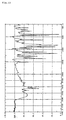
- Fig. 1 is a X-ray diffraction spectrum of I-form dimer, which is prepared in Synthesis Example 4.
- Fig. 2 is a X-ray diffraction spectrum of Pseudo II-form dimer, which is prepared in Example 1.
- Fig. 3 is a X-ray diffraction spectrum of II-form dimer of the present invention.
- Fig. 4 is a X-ray diffraction spectrum of III-form dimer of the present invention.
- Fig. 5 is a X-ray diffraction spectrum of IV-form dimer of the present invention.
- Fig. 6 is a TOF-MS spectrum of ⁇ -oxo-aluminum phthalocyanine dimer of the present invention.
- Fig. 7 is a X-ray diffraction spectrum of chloroaluminum Pc, which is prepared in Synthesis Example 1.
- Fig. 8 is a X-ray diffraction spectrum of chloroaluminum Pc, which is prepared in Synthesis Example 2.
- Fig. 9 is a X-ray diffraction spectrum of hydroxyaluminum Pc, which is prepared in Synthesis Example 3.
- Fig. 10 is an infrared absorption spectrum of I-form ⁇ -oxo-aluminum Pc dimer, which is prepared in Synthesis Example 4.
- Fig. 11 is an infrared absorption spectrum of Pseudo II-form ⁇ -oxo-aluminum Pc dimer, which is prepared in Example 1.
- Fig. 12 is an infrared absorption spectrum of II-form ⁇ -oxo-aluminum Pc dimer of the present invention.
- Fig. 13 is an infrared absorption spectrum of III-form ⁇ -oxo-aluminum Pc dimer of the present invention.
- Fig. 14 is an infrared absorption spectrum of IV-form ⁇ -oxo-aluminum Pc dimer of the present invention.
- Fig. 15 is a plot of results obtained by a spectroscopic sensitivity analysis of photoreceptors prepared in Examples 15 and 19, and Comparative Examples 1 and 2.
- Fig. 16 is a plot of results obtained by a potential durability analysis of photoreceptors which is prepared in Examples 15 and 19, and Comparative Examples 1 and 2.
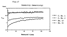
- Fig. 17 is a plot of results obtained by a sensitivity durability analysis of photoreceptors which is prepared in Examples 15 and 19, and Comparative Examples 1 and 2.
- I-Form dimer is known in the art and it is prepared by, for example, the process described below.
- the wording "I-form dimer" means ⁇ -oxo-aluminum phthalocyanine dimer having conventional polymorph, throughout the specification.
- Phthalonitrile or 1,3-diiminoisoindoline is reacted in the presence of aluminum chloride in organic solvent having a high boiling point such as 1-chloronaphtalene and quinoline to obtain chloroaluminum phthalocyanine.
- the crude chloroaluminum Pc is then purified. That is, it is refluxed with stirring in toluene or 1,3-dioxosilane for about 3 hours, and rinsed with toluene or acetone two or three times. It is then dispersed in ion-exchanged water, stirred at 60 to 70°C for 1 hour, filtered, rinsed with water, and dried under vacuum.
- the resulting chloroaluminum Pc is hydrolyzed to obtain hydroxyaluminum Pc.
- the process of hydrolysis is known to the art and described in JP-A-5-93150/1993, and JP-A-6-214415/1994 for example.
- the chloroaluminum Pc is hydrolyzed in an acidic or a basic solution, or subjected to acid pasting to prepare hydroxyaluminum Pc.
- the resulting hydroxyaluminum Pc is refluxed with stirring in a water immiscible organic solvent such as o-dichlorobenzene, generated water is then excluded from the reaction system, and the product (I-form dimer) is collected by filtration. The product is then washed with DMF and then methanol etc., dried, and ground to obtain the I-form dimer.
- the I-Form dimer (PcAl-O-AlPc) or hydroxyaluminum Pc (HO-AlPc) may specifically be prepared from chloroaluminum Pc (Cl-AlPc) by the method which is described in J. E. Owen; M. E. Kenny, Inorg. Chem., 1, 331-333, 1962.
- the I-form dimer is dry milled at first.
- dry mill or “dry milling” of the present specification means the step in which the substance is milled by using no solvent, but optionally using a mill medium, on a dispersing machine such as a ball mill, a sand mill, a paint shaker, an attritor, and an automatic mortar.
- a dispersing machine such as a ball mill, a sand mill, a paint shaker, an attritor, and an automatic mortar.
- the mill medium include glass beads, steel beads, and alumina beads.
- the resulting ⁇ -oxo-aluminum Pc dimer is no longer the I-form dimer. It has a novel polymorph which shows diffraction peaks at a Bragg angle (2 ⁇ ⁇ 0.2°) of 6.8°, 15.4°, and 24.0° in a X-ray diffraction spectrum by CuK ⁇ -ray.
- the ⁇ -oxo-aluminum Pc dimer having the novel polymorph is referred to as "Pseudo II-form dimer”
- the novel polymorph is referred to as "Pseudo II-form polymorph", in the specification.
- the dry milling is conducted generally at room temperature for 10 to 100 hours, preferably 24 to 48 hours. If the dry milling is conducted less than 10 hours, formation of the polymorph may become insufficient, and even if the dry milling is conducted more than 100 hours,a useful effect may not be obtained. According to the milling procedure, the Pseudo II-form dimer becomes somewhat amorphous.
- the dry milling is for example conducted by using a dispersing machine (a paint shaker for example), until the polymorph becomes fixed.
- a dispersing machine a paint shaker for example
- the resulting Pseudo II-form dimer shows diffraction peaks at a Bragg angle (2 ⁇ ⁇ 0.2°) of 6.8°, 15.4°, and 24.0° in a X-ray diffraction spectrum.
- the polymorph is novel.
- the Pseudo II-form dimer may be employed as a charge generator for an electrophotographic photoreceptor as described below.
- ⁇ -Oxo-aluminum Pc dimer which has a novel polymorph may further be obtained by using the Pseudo II-form dimer.
- the Pseudo II-form dimer is wet milled or simply dispersed in a solvent, in that case.
- wet mill or “wet milling” of the present specification means the step in which the substance is milled by using a solvent. Wet milling is conducted in substantially the same manner as the dry milling, except using a solvent. Thus, a mill medium such as glass beads, steel beads, and alumina beads may be employed in the wet milling.
- a mill medium such as glass beads, steel beads, and alumina beads may be employed in the wet milling.
- disperse or “simply dispersing” means the step in which the substance is dispersed with stirring into a solvent. The simply dispersing may optionally be conducted with heating.
- the wet milling or simply dispersing is conducted generally at room temperature for 20 to 100 hours, preferably 24 to 48 hours. If the step is conducted less than 10 hours, formation of the polymorph may become insufficient, and even if the wet milling is conducted more than 100 hours, useful effect may not be obtained.
- the wet milling is conducted by using a solvent, until polymorph become fixed.
- ethanol used as the solvent, it takes about 72 hours.
- the simply dispersing is conducted by using a solvent, until polymorph becomes fixed.
- cyclohexanone for example, it takes about 12 hours under reflux.
- diethylene glycol is used as the solvent, it takes about 7 hours at 100°C.
- diglyme is used as the solvent, it takes about 11 hours at 162°C.
- a solvent employed in the present invention is not particularly limited, unless it dissolves the pigment.
- the solvent is generally selected, depending on a kind of the desired polymorph, from a ketone solvent, an alcohol solvent, a glycol solvent, a formamide solvent, an ether solvent, and an aromatic solvent.
- ketone solvent examples include linear or cyclic ketones such as cyclohexanone, diisopropyl ketone, methyl ethyl ketone (MEK), methyl isobutyl ketone (MIBK).
- alcohol solvent examples include monohydric lower alcohols such as methanol, ethanol, propanol, isopropanol, and amyl alcohol.
- glycol solvent examples include alkylene glycols such as ethylene glycol, diethylene glycol, and trimethylene glycol; alkylene glycol monoalkyl ethers such as ethylene glycol monomethyl ether, ethylene glycol monoethyl ether, propylene glycol monomethyl ether; ethylene glycol dialkyl ethers such as monoglyme, diglyme, triglyme, and tetraglyme.
- formamide solvent include dimethylformamide (DMF), and dimethylacetamide.
- ether solvent examples include linear or cyclic ethers such as tetrahydrofuran (THF), dioxane, ethyl ether, and butyl ether.
- aromatic solvent examples include hydrocarbon solvents such as toluene, o-xylene, and tetralin.
- the II-form dimer When the Pseudo II-form dimer is wet milled or simply dispersed in the ketone solvent such as cyclohexanone and diisopropyl ketone, preferably cyclohexanone; the alcohol solvent such as amyl alcohol, and ethanol; the glycol solvent such as DMF; and the ether solvent such as THF; the II-form dimer having II-form polymorph is obtained.
- a X-ray diffraction spectrum of the II-form dimer is shown in Fig. 3. The spectrum of Fig. 3 is clearly different from that of Fig. 1, and the polymorph of II-form dimer is different from that of I-form dimer.
- the II-form dimer may be employed as a charge generator for an electrophotographic photoreceptor as described below, and it has good photosensitive property.
- III-form dimer When the Pseudo II-form dimer is wet milled or simply dispersed in the glycol solvent such as ethylene glycol, ⁇ -oxo-aluminum Pc dimer having a novel polymorph which shows diffraction peaks at a Bragg angle (2 ⁇ ⁇ 0.2°) of 6.9°, 14.0°, 15.7°, and 25.7° in a X-ray diffraction spectrum is obtained.
- the ⁇ -oxo-aluminum Pc dimer having the novel polymorph is referred to as "III-form dimer".
- a X-ray diffraction spectrum of the III-form dimer is shown in Fig. 4.
- the spectrum of Fig. 4 is clearly different from that of Fig. 1, and the polymorph of III-form dimer is different from that of I-form dimer.
- III-Form dimer may be employed as a charge generator for an electrophotographic photoreceptor as described below.
- ⁇ -oxo-aluminum Pc dimer having a novel polymorph which shows diffraction peaks at a Bragg angle (2 ⁇ ⁇ 0.2°) of 6.9°, 13.0°, 14.8°, 16.1°, 21.1°, 25.1° and 25.8° in a X-ray diffraction spectrum, is obtained.
- the ⁇ -oxo-aluminum Pc dimer having the novel polymorph is referred to as "IV-form dimer".
- IV-Form dimer may be employed as a charge generator for an electrophotographic photoreceptor as described below.
- ⁇ -Oxo-aluminum Pc dimer having a novel polymorph of the present invention is preferably employed as a photoconductive material for use in an electrophotographic photoreceptor which is widely applied to a copying machine using electrophotographic technology.
- the photoconductive material comprising ⁇ -oxo-aluminum Pc dimer of the present invention as an effective ingredient provides good chargeability, high sensitivity, and high durability, when it is applied as a charge generating layer of an electrophotographic receptor.
- the electrophotographic receptor generally has a conductive substrate, and a photoconductive layer formed thereon which comprises a charge generator and a charge transporting material.
- the photoconductive layer may be classified depending on its structure, i.e., a mono-layered one and a bi-layered one.
- ⁇ -Oxo-aluminum Pc dimer of the present invention may be employed in both the mono-layered photoconductive layer and the bi-layered photoconductive layer.
- ⁇ -oxo-aluminum Pc dimer of the present invention is applied to the bi-layered photoconductive layer, because each of the layers in the bi-layered photoconductive layer do not inhibit the respective functions, and they efficiently transfer the generated charge to a surface of the electrophotographic photoreceptor without trapping the charge, and therefore, electronic properties of the ⁇ -oxo-aluminum Pc dimer may sufficiently be exhibited.
- the electrophotographic photoreceptor which has bi-layered construction is generally called as a function separated-form photoreceptor.
- the function separated-form photoreceptor is prepared by, for example, forming a charge generating layer on a conductive substrate, and forming a charge transporting layer thereon.
- the conductive substrate include metal (e.g., aluminum, nickel), metal vapor-deposited film and the like, in the form of a drum, a sheet or a belt.
- ⁇ -oxo-aluminum Pc dimer of the present invention may be included as a charge generator in the charge generating layer.
- the charge generating layer is formed as a thin layer on the conductive substrate. It can be formed by vapor-depositing the ⁇ -oxo-aluminum Pc dimer, but is generally formed by applying a binder resin dispersion of the ⁇ -oxo-aluminum Pc dimer.
- the binder resin dispersion may be prepared by dispersing the ⁇ -oxo-aluminum Pc dimer into a solution of a suitable binder resin, using a usual dispersing apparatus such as ball mill, sand mill, paint shaker and the like.
- a process for coating the binder resin dispersion is not specifically limited, and suitably include bar coating, dip coating, spin coating, roller coating, calendar coating and the like.
- the coated layer may be dried at a temperature of 30 to 200°C for 5 minutes to 2 hours in the presence or absence of blast.
- a solvent optionally be employed for preparing the dispersion.
- the solvent employed in the present invention is not particularly limited, unless it dissolves the pigment.
- a solvent which may disperse a pigment uniformly and may solve a binder resin is preferred.
- examples thereof include alcohol solvents such as methanol, ethanol, isopropanol and butanol; aromatic solvents such as toluene, xylene and tetralin; halogenated solvents such as dichloromethane, chloroform, trichloroethylene and carbon tetrachloride; ester solvents such as ethyl acetate and propyl acetate; ether solvents such as ethylene glycol monoethyl ether, dioxane and tetrahydrofuran; dimethylformamide and dimethyl sulfoxide.
- the binder resin can be selected from a wide range of insulating resins.
- the preferred resin include condensation resins such as polycarbonate, polyacrylate, polyester and polyamide; addition polymers such as polystyrene, styrene-acrylic copolymer, polyacrylate, polymethacrylate, polyvinyl butyral, polyvinyl alcohol, polyacrylonitrile, polyacrylic-butadiene copolymer, polyvinyl chloride and vinyl chloride-vinyl acetate copolymer; organic photoconductive resins such as poly-N-vinyl carbazole and polyvinylanthracene; polysulfone, polyether sulfone, silicone resin, epoxy resin and urethane resin. These are used alone or in combination thereof.
- the binder resin is employed in an amount of from 0.1 to 3 ratio by weight, preferably 0.5 to 2.0 by weight based on the charge generator. When the amount is more than 3, the amount of charge may decrease, and sensitivity of the photoconductive layer may become poor.
- the charge generating layer is preferably formed in a thickness of from 0.05 to 5.0 ⁇ m, preferably 0.1 to 3.0 ⁇ m. When the thickness is more than 5.0 ⁇ m, charge may readily be trapped, and the sensitivity of the photoconductive layer may become poor.
- a charge transporting layer containing a charge transporting material is then formed on the charge generating layer.
- This layer may be formed in the same manner as described above, for forming the charge generating layer. That is, the charge transporting material is dissolved in a solvent with a binder resin, and the resulting solution is uniformly applied on the charge generating layer, followed by drying.
- Examples of the charge transporting material include conventional materials such as an oxadiazole derivative, a pyrazoline derivative, a hydrazone derivative, a triazine derivative, a quinazoline derivative, a triarylamine compound, a styryltriphenylamine compound, a butadiene compound, and a carbazole compound.
- binder resin and solvent examples include the same materials as that employed for the charge generating layer.
- the binder resin is employed in an amount of from 0.1 to 5 ratio by weight, preferably 0.5 to 2.0 ratio by weight based on the charge transporting material. When the amount is more than 5, concentration of the charge transporting material in the charge transporting layer may become small, and sensitivity of the photoconductive layer may become poor.
- the charge transporting layer is preferably formed in a thickness of from 5 to 50 ⁇ m, preferably 10 to 40 ⁇ m. When the thickness is more than 50 ⁇ m, a long time may be required for transporting charge, and the charge may be trapped, and thereby the sensitivity of the photoconductive layer may become poor.
- the X-ray diffraction spectrum by CuK ⁇ -ray was measured by using the automatic X-ray diffraction system "MXP3" manufactured by Max Science Co. Ltd., and TOF-MS (Time of Flight Mass Spectroscopy) was measured by using "COMPACT MALDI III” manufactured by Kratos-Shimazu Co. Ltd., in the detection mode “Positive”, the voltage “Low (5 kV)", and the flying mode "Reflection", in the Examples.
- Chloroaluminum Pc was prepared according to substantially the same manner as described in Synthesis Example 1, except that 1,3-dioxosilane was used as a solvent for dispersing and washing instead of toluene.
- the product was 61.1 g (yield 90.8%) of blue solid.
- a X-ray diffraction spectrum of the product was shown in Fig. 8.
- Example II-form dimer of the present invention was prepared according to substantially the same manner as described in Example 2, except that the solvent tabulated in table 4 was used instead of cyclohexanone, and the conditions tabulated in table 4 were used.
- the present example illustrates a function separated-form electrophotographic photoreceptor to which the ⁇ -oxo-aluminum Pc dimer having a novel polymorph of the present invention was applied.
- the Pseudo II-form dimer prepared in Example 1 was employed as a charge generator (CG material).
- 0.2 g of the Pseudo II-form dimer, 0.2 g of a polyvinyl butyral resin ("Elex BH-3" available from Sekisui Kagaku K.K.), 59.6 g of cyclohexanone, and 50 g of glass beads having a diameter of 3 mm ⁇ were charged in a wide-mouthed bottle.
- the mixture was shook for 1 hour using a dispersing apparatus (paint shaker), and applied on an aluminum plate by a bar coater.
- the coating was dried in air to form a charge generating layer having a thickness of 0.5 ⁇ m.
- An electrophotographic photoreceptor was prepared according to substantially the same manner as described in Example 13, except that 4-benzylamino-2-methylbenzaldehyde-1,1'-diphenylhydorazone ("CTC-191" manufactured by Takasa Koryo K.K.) was used as CT material instead of 1,1-bis(p-diethylaminophenyl)-4,4'-diphenyl-1,3-butadiene.
- CTC-191 4-benzylamino-2-methylbenzaldehyde-1,1'-diphenylhydorazone
- CT material 1,1-bis(p-diethylaminophenyl)-4,4'-diphenyl-1,3-butadiene.
- Electrophotographic photoreceptors of the present invention were prepared according to substantially the same manner as described in Example 13, except that the materials tabulated in the following Table 8 were used as CG material and CT material.
- An electrophotographic photoreceptor was prepared according to substantially the same manner as described in Example 14, except that Y-form titanyl Pc which was prepared according to the procedure described in JP-B-3-35064/1991 (Konica K.K.) was used as CG material instead of the Pseudo II-form dimer.
- An electrophotographic photoreceptor was prepared according to substantially the same manner as described in Example 13, except that X-form nonmetallo-Pc which was prepared according to the procedure described in JP-B-3-78872/1991 was used in CG material instead of the Pseudo II-form dimer.
- An electrophotographic photoreceptor was prepared according to substantially the same manner as described in Example 14, except that hydroxyaluminum Pc which was prepared according to the procedure described in JP-A-5-93150/1993 (Fuji Xerox K.K.) was used as CG material instead of the Pseudo II-form dimer.
- An electrophotographic photoreceptor was prepared according to substantially the same manner as described in Example 13, except that the I-form dimer which was prepared in Synthesis Example 4 was used as CG material instead of the Pseudo II-form dimer.
- An electrophotographic photoreceptor was prepared according to substantially the same manner as described in Example 13, except that the I-form dimer which was prepared in Synthesis Example 4 was used as CG material, and 4-dibenzylamino-2-methylbenzaldehyde-1,1-diphenylhydrazone was used as CT material.
- Electrophotographic property of the photoconductors prepared in Examples 13 to 36 and Comparative Examples 1 to 5 were measured.
- a static electricity charging tester "EPA-8200" manufactured by Kawaguchi Denki K.K. was used as the measuring apparatus.
- the sample was corona charged at -8.0 kV in STAT 3 mode by first. It was then left in the dark for 20 seconds, and irradiated by 5.0 lux white light for 10.0 seconds.
- the charged potential (Vo), the sensitivity half-value irradiation amount (E 1/2 ), the residual potential (Vr) were recorded. The results were shown in Tables 8 and 9. Table 8 Example No.
- the photoreceptors of the examples show excellent photoconductive property. Particularly, those which employ the II-form dimer polymorphied by amyl alcohol or cyclohexanone (Examples 15, 16, 19 and 20) show high photoconductivity in good reproductivity. On the other hand, the Comparative Examples which employ the conventional CG materials such as Y-form titanyl Pc and X-form nonmetallo-Pc, show poor photosensitive properties. Thus, the ⁇ -oxo-aluminum Pc dimer having a novel polymorph of the present invention has high performance suitable for the practical use as a CG material. The inventors are now further investigating a binder and a CT material which well match with the present ⁇ -oxo-aluminum Pc dimer.
- the photoconductors of Examples 15 and 19, and Comparative Example 1 and 2 were corona charged as described above and discharged, 100 times.
- Fig. 15 Change of charged potential (Vo), and Residual potential (Vr) during the procedure of charging and discharging was shown in Fig. 16 and 17, respectively.
- ⁇ -oxo-aluminum Pc dimer having novel polymorph of the present invention is useful as a photoconductive materials for use in the related art of optoelectronics.
Landscapes
- Chemical & Material Sciences (AREA)
- Chemical Kinetics & Catalysis (AREA)
- Organic Chemistry (AREA)
- Physics & Mathematics (AREA)
- General Physics & Mathematics (AREA)
- Photoreceptors In Electrophotography (AREA)
Applications Claiming Priority (3)
| Application Number | Priority Date | Filing Date | Title |
|---|---|---|---|
| JP25206/96 | 1996-02-13 | ||
| JP02520696A JP3967397B2 (ja) | 1996-02-13 | 1996-02-13 | 新規な結晶変態を有するμ−オキソ−アルミニウムフタロシアニンダイマー及びこれを用いた電子写真感光体 |
| JP2520696 | 1996-02-13 |
Publications (3)
| Publication Number | Publication Date |
|---|---|
| EP0790283A2 true EP0790283A2 (de) | 1997-08-20 |
| EP0790283A3 EP0790283A3 (de) | 1997-12-10 |
| EP0790283B1 EP0790283B1 (de) | 2002-12-11 |
Family
ID=12159489
Family Applications (1)
| Application Number | Title | Priority Date | Filing Date |
|---|---|---|---|
| EP97102314A Expired - Lifetime EP0790283B1 (de) | 1996-02-13 | 1997-02-13 | Mu-oxo-Aluminiumphthalocyanindimer mit einem neuen Polymorph und damit hergestellter elektrophotographischer Photorezeptor |
Country Status (4)
| Country | Link |
|---|---|
| US (1) | US5725984A (de) |
| EP (1) | EP0790283B1 (de) |
| JP (1) | JP3967397B2 (de) |
| DE (1) | DE69717694T2 (de) |
Cited By (4)
| Publication number | Priority date | Publication date | Assignee | Title |
|---|---|---|---|---|
| EP0835912A1 (de) * | 1996-09-13 | 1998-04-15 | Orient Chemical Industries, Ltd. | Mu-oxo-Galliumphthalocyaninedimer mit einem neuen Polymorph und damit hergestellter elektrophotographischer Photorezeptor |
| EP1004634A2 (de) * | 1998-11-26 | 2000-05-31 | Orient Chemical Industries, Ltd. | My-Oxo-Aluminium/Gallium Phthalocyanin Dimer |
| EP1018505A2 (de) * | 1999-01-08 | 2000-07-12 | Orient Chemical Industries, Ltd. | Verfahren zur Herstellung eines Triarylamindimers |
| WO2006048388A3 (en) * | 2004-11-01 | 2006-07-06 | Ciba Sc Holding Ag | Highly concentrated flowable pigment composition and process for its manufacture |
Families Citing this family (2)
| Publication number | Priority date | Publication date | Assignee | Title |
|---|---|---|---|---|
| JP3939425B2 (ja) * | 1998-03-10 | 2007-07-04 | オリヱント化学工業株式会社 | 積層型電子写真感光体 |
| TWI455215B (zh) * | 2009-06-11 | 2014-10-01 | Advanced Semiconductor Eng | 半導體封裝件及其之製造方法 |
Citations (2)
| Publication number | Priority date | Publication date | Assignee | Title |
|---|---|---|---|---|
| GB2255980A (en) * | 1991-04-26 | 1992-11-25 | Fuji Xerox Co Ltd | Hydroxygallium phthocyanine |
| US5456998A (en) * | 1994-04-26 | 1995-10-10 | Xerox Corporation | Photoconductive imaging members containing alkoxy-bridged metallophthalocyanine dimers |
Family Cites Families (6)
| Publication number | Priority date | Publication date | Assignee | Title |
|---|---|---|---|---|
| DE3469611D1 (en) * | 1983-06-30 | 1988-04-07 | Eastman Kodak Co | Hydroxyaluminumphthalocyanine having reduced green absorption |
| JPS60254044A (ja) * | 1984-05-30 | 1985-12-14 | Toshiba Corp | 電子写真感光体 |
| CA1279787C (en) * | 1985-12-06 | 1991-02-05 | Tatsuro Iwabuchi | Electrophotographic photoconductor using phthalocyanine compound |
| US5039798A (en) * | 1990-03-01 | 1991-08-13 | Hoechst Celanese Corp. | Oxygen bridged naphthalocyanine dimers and their use in optical information storage media |
| JPH0593150A (ja) * | 1991-04-22 | 1993-04-16 | Fuji Xerox Co Ltd | ヒドロキシアルミニウムフタロシアニンの新規結晶、該新規結晶よりなる光導電材料及びそれを用いた電子写真感光体 |
| JP3218770B2 (ja) * | 1993-01-14 | 2001-10-15 | 富士ゼロックス株式会社 | 電子写真感光体とそのためのフタロシアニン顔料および顔料分散液 |
-
1996
- 1996-02-13 JP JP02520696A patent/JP3967397B2/ja not_active Expired - Fee Related
-
1997
- 1997-02-12 US US08/799,419 patent/US5725984A/en not_active Expired - Lifetime
- 1997-02-13 DE DE69717694T patent/DE69717694T2/de not_active Expired - Lifetime
- 1997-02-13 EP EP97102314A patent/EP0790283B1/de not_active Expired - Lifetime
Patent Citations (2)
| Publication number | Priority date | Publication date | Assignee | Title |
|---|---|---|---|---|
| GB2255980A (en) * | 1991-04-26 | 1992-11-25 | Fuji Xerox Co Ltd | Hydroxygallium phthocyanine |
| US5456998A (en) * | 1994-04-26 | 1995-10-10 | Xerox Corporation | Photoconductive imaging members containing alkoxy-bridged metallophthalocyanine dimers |
Non-Patent Citations (4)
| Title |
|---|
| DATABASE WPI Section Ch, Week 9320 Derwent Publications Ltd., London, GB; Class E23, AN 93-162226 XP002043487 & JP 05 093 150 A (FUJI XEROX CO LTD) , 16 April 1993 * |
| DATABASE WPI Section Ch, Week 9436 Derwent Publications Ltd., London, GB; Class A89, AN 94-288229 XP002043488 & JP 06 214 415 A (FUJI XEROX CO LTD) , 5 August 1994 * |
| J.E OWEN ET AL: "Aluminium and silicon hydroxy and oxy systems of the phthalocyanino type" INORGANIC CHEMISTRY, no. 1, 1962, EASTON, US, pages 334-336, XP002043486 * |
| OWEN, J. E.; KENNY, M. E. INORG. CHEM. vol. 1, 1962, pages 331 - 333 * |
Cited By (9)
| Publication number | Priority date | Publication date | Assignee | Title |
|---|---|---|---|---|
| EP0835912A1 (de) * | 1996-09-13 | 1998-04-15 | Orient Chemical Industries, Ltd. | Mu-oxo-Galliumphthalocyaninedimer mit einem neuen Polymorph und damit hergestellter elektrophotographischer Photorezeptor |
| US5910384A (en) * | 1996-09-13 | 1999-06-08 | Orient Chemical Industries, Ltd. | μ -oxo-galliuim phthalocyanine dimer having novel polymorph and electrophotographic photoreceptor prepared by using the same |
| US5981745A (en) * | 1996-09-13 | 1999-11-09 | Orient Chemical Industries, Ltd. | μ-oxo-gallium phthalocyanine dimer having novel polymorph and electrophotographic photoreceptor prepared by using the same |
| EP1004634A2 (de) * | 1998-11-26 | 2000-05-31 | Orient Chemical Industries, Ltd. | My-Oxo-Aluminium/Gallium Phthalocyanin Dimer |
| EP1004634A3 (de) * | 1998-11-26 | 2002-03-06 | Orient Chemical Industries, Ltd. | My-Oxo-Aluminium/Gallium Phthalocyanin Dimer |
| EP1018505A2 (de) * | 1999-01-08 | 2000-07-12 | Orient Chemical Industries, Ltd. | Verfahren zur Herstellung eines Triarylamindimers |
| EP1018505A3 (de) * | 1999-01-08 | 2000-09-13 | Orient Chemical Industries, Ltd. | Verfahren zur Herstellung eines Triarylamindimeres |
| WO2006048388A3 (en) * | 2004-11-01 | 2006-07-06 | Ciba Sc Holding Ag | Highly concentrated flowable pigment composition and process for its manufacture |
| EP2502965A1 (de) * | 2004-11-01 | 2012-09-26 | Basf Se | Hochkonzentrierte fließfähige Pigmentzusammensetzung und Verfahren zu ihrer Herstellung |
Also Published As
| Publication number | Publication date |
|---|---|
| DE69717694D1 (de) | 2003-01-23 |
| JP3967397B2 (ja) | 2007-08-29 |
| EP0790283A3 (de) | 1997-12-10 |
| EP0790283B1 (de) | 2002-12-11 |
| DE69717694T2 (de) | 2003-10-16 |
| US5725984A (en) | 1998-03-10 |
| JPH09217020A (ja) | 1997-08-19 |
Similar Documents
| Publication | Publication Date | Title |
|---|---|---|
| JP2561940B2 (ja) | ガリウムフタロシアニン化合物およびそれを用いた電子写真感光体 | |
| US5563261A (en) | Hydroxygallium phthalocyanine photoconductive imaging members | |
| US5834149A (en) | Hydroxygallium phthalocyanine crystals and electrophotographic photoreceptors using same | |
| JPH0629975B2 (ja) | 積層型電子写真用感光体 | |
| JPH0629976B2 (ja) | 単層型電子写真用感光体 | |
| EP0835912B1 (de) | My-oxo-Galliumphthalocyanindimer mit einem neuen Polymorph und damit hergestellter elektrophotographischer Photorezeptor | |
| JPH061386B2 (ja) | 光半導体材料およびこれを用いた電子写真感光体 | |
| JPS63116158A (ja) | 光半導体材料およびこれを用いた電子写真感光体 | |
| US5668276A (en) | Hydroxygallium phthalocyanine processes | |
| EP0790283B1 (de) | Mu-oxo-Aluminiumphthalocyanindimer mit einem neuen Polymorph und damit hergestellter elektrophotographischer Photorezeptor | |
| JPH05194523A (ja) | クロロガリウムフタロシアニンの新規な結晶の製造方法及びその結晶を用いた電子写真感光体 | |
| EP1004634B1 (de) | My-Oxo-Aluminium/Gallium Phthalocyanin Dimer | |
| US5292604A (en) | Phthalocyanine crystal of mixed pigments and electrophotographic photoreceptor using the same | |
| JP4450911B2 (ja) | μ−オキソ−アルミニウム/ガリウムフタロシアニン二量体 | |
| US5420268A (en) | Oxytitanium phthalocyanine imaging members and processes thereof | |
| KR100983758B1 (ko) | 유기 전자 사진의 광-수용체 | |
| US5534376A (en) | Tetrafluoro hydroxygallium phthalocyanines and photoconductive imaging members | |
| JP4467596B2 (ja) | μ−オキソ−アルミニウムフタロシアニンダイマーの製造方法 | |
| US6180301B1 (en) | Tetrafluoro hydroxygallium phthalocyanines and photoconductive imaging members | |
| US6106985A (en) | Layered-form electrophotographic photoreceptor | |
| JPH01144057A (ja) | 光半導体材料およびこれを用いた電子写真感光体 | |
| JP2542716B2 (ja) | ε型ニッケルフタロシアニン化合物およびそれを用いた電子写真感光体 | |
| US5491228A (en) | Preparative processes for dihydroxygermanium phthalocyanine | |
| US5382493A (en) | Hydroxygermanium phthalocyanine processes | |
| JPH01247464A (ja) | ε型亜鉛フタロシアニン化合物およびそれを用いた電子写真感光体 |
Legal Events
| Date | Code | Title | Description |
|---|---|---|---|
| PUAI | Public reference made under article 153(3) epc to a published international application that has entered the european phase |
Free format text: ORIGINAL CODE: 0009012 |
|
| AK | Designated contracting states |
Kind code of ref document: A2 Designated state(s): CH DE FR GB LI |
|
| PUAL | Search report despatched |
Free format text: ORIGINAL CODE: 0009013 |
|
| AK | Designated contracting states |
Kind code of ref document: A3 Designated state(s): CH DE FR GB LI |
|
| 17P | Request for examination filed |
Effective date: 19980129 |
|
| 17Q | First examination report despatched |
Effective date: 20000720 |
|
| GRAG | Despatch of communication of intention to grant |
Free format text: ORIGINAL CODE: EPIDOS AGRA |
|
| GRAG | Despatch of communication of intention to grant |
Free format text: ORIGINAL CODE: EPIDOS AGRA |
|
| GRAG | Despatch of communication of intention to grant |
Free format text: ORIGINAL CODE: EPIDOS AGRA |
|
| GRAH | Despatch of communication of intention to grant a patent |
Free format text: ORIGINAL CODE: EPIDOS IGRA |
|
| GRAH | Despatch of communication of intention to grant a patent |
Free format text: ORIGINAL CODE: EPIDOS IGRA |
|
| GRAA | (expected) grant |
Free format text: ORIGINAL CODE: 0009210 |
|
| AK | Designated contracting states |
Kind code of ref document: B1 Designated state(s): CH DE FR GB LI |
|
| REG | Reference to a national code |
Ref country code: GB Ref legal event code: FG4D |
|
| REG | Reference to a national code |
Ref country code: CH Ref legal event code: EP |
|
| REF | Corresponds to: |
Ref document number: 69717694 Country of ref document: DE Date of ref document: 20030123 |
|
| PGFP | Annual fee paid to national office [announced via postgrant information from national office to epo] |
Ref country code: GB Payment date: 20030207 Year of fee payment: 7 |
|
| PGFP | Annual fee paid to national office [announced via postgrant information from national office to epo] |
Ref country code: CH Payment date: 20030219 Year of fee payment: 7 |
|
| PGFP | Annual fee paid to national office [announced via postgrant information from national office to epo] |
Ref country code: FR Payment date: 20030226 Year of fee payment: 7 |
|
| REG | Reference to a national code |
Ref country code: CH Ref legal event code: NV Representative=s name: A. BRAUN, BRAUN, HERITIER, ESCHMANN AG PATENTANWAE |
|
| ET | Fr: translation filed | ||
| PLBE | No opposition filed within time limit |
Free format text: ORIGINAL CODE: 0009261 |
|
| STAA | Information on the status of an ep patent application or granted ep patent |
Free format text: STATUS: NO OPPOSITION FILED WITHIN TIME LIMIT |
|
| 26N | No opposition filed |
Effective date: 20030912 |
|
| PG25 | Lapsed in a contracting state [announced via postgrant information from national office to epo] |
Ref country code: GB Free format text: LAPSE BECAUSE OF NON-PAYMENT OF DUE FEES Effective date: 20040213 |
|
| PG25 | Lapsed in a contracting state [announced via postgrant information from national office to epo] |
Ref country code: LI Free format text: LAPSE BECAUSE OF NON-PAYMENT OF DUE FEES Effective date: 20040229 Ref country code: CH Free format text: LAPSE BECAUSE OF NON-PAYMENT OF DUE FEES Effective date: 20040229 |
|
| GBPC | Gb: european patent ceased through non-payment of renewal fee |
Effective date: 20040213 |
|
| REG | Reference to a national code |
Ref country code: CH Ref legal event code: PL |
|
| PG25 | Lapsed in a contracting state [announced via postgrant information from national office to epo] |
Ref country code: FR Free format text: LAPSE BECAUSE OF NON-PAYMENT OF DUE FEES Effective date: 20041029 |
|
| REG | Reference to a national code |
Ref country code: FR Ref legal event code: ST |
|
| PGFP | Annual fee paid to national office [announced via postgrant information from national office to epo] |
Ref country code: DE Payment date: 20120330 Year of fee payment: 16 |
|
| REG | Reference to a national code |
Ref country code: DE Ref legal event code: R119 Ref document number: 69717694 Country of ref document: DE Effective date: 20130903 |
|
| PG25 | Lapsed in a contracting state [announced via postgrant information from national office to epo] |
Ref country code: DE Free format text: LAPSE BECAUSE OF NON-PAYMENT OF DUE FEES Effective date: 20130903 |