EP0784399A1 - Dispositif de prise de vues - Google Patents
Dispositif de prise de vues Download PDFInfo
- Publication number
- EP0784399A1 EP0784399A1 EP95932941A EP95932941A EP0784399A1 EP 0784399 A1 EP0784399 A1 EP 0784399A1 EP 95932941 A EP95932941 A EP 95932941A EP 95932941 A EP95932941 A EP 95932941A EP 0784399 A1 EP0784399 A1 EP 0784399A1
- Authority
- EP
- European Patent Office
- Prior art keywords
- gradation compensation
- gradation
- signal
- image
- gain
- Prior art date
- Legal status (The legal status is an assumption and is not a legal conclusion. Google has not performed a legal analysis and makes no representation as to the accuracy of the status listed.)
- Granted
Links
- 238000011156 evaluation Methods 0.000 claims abstract description 61
- 238000003384 imaging method Methods 0.000 claims description 96
- 238000012545 processing Methods 0.000 claims description 86
- 230000009467 reduction Effects 0.000 claims description 52
- 230000001629 suppression Effects 0.000 claims description 47
- 238000000605 extraction Methods 0.000 claims description 44
- 238000010586 diagram Methods 0.000 description 39
- 238000000034 method Methods 0.000 description 37
- 230000008569 process Effects 0.000 description 30
- 230000010354 integration Effects 0.000 description 20
- 238000012937 correction Methods 0.000 description 17
- 230000001276 controlling effect Effects 0.000 description 14
- 230000003111 delayed effect Effects 0.000 description 8
- 238000012935 Averaging Methods 0.000 description 7
- 230000000694 effects Effects 0.000 description 7
- 238000013139 quantization Methods 0.000 description 7
- 230000008859 change Effects 0.000 description 5
- 239000011159 matrix material Substances 0.000 description 5
- 230000001934 delay Effects 0.000 description 4
- 210000003127 knee Anatomy 0.000 description 4
- 238000010606 normalization Methods 0.000 description 4
- 238000001914 filtration Methods 0.000 description 3
- 238000003709 image segmentation Methods 0.000 description 3
- 230000007246 mechanism Effects 0.000 description 3
- 230000015556 catabolic process Effects 0.000 description 2
- 238000006731 degradation reaction Methods 0.000 description 2
- 238000013461 design Methods 0.000 description 2
- 230000001105 regulatory effect Effects 0.000 description 2
- 238000013528 artificial neural network Methods 0.000 description 1
- 238000006243 chemical reaction Methods 0.000 description 1
- 239000002131 composite material Substances 0.000 description 1
- 230000000593 degrading effect Effects 0.000 description 1
- 230000006866 deterioration Effects 0.000 description 1
- 230000006872 improvement Effects 0.000 description 1
- 238000002156 mixing Methods 0.000 description 1
- 238000012986 modification Methods 0.000 description 1
- 230000004048 modification Effects 0.000 description 1
Images


Classifications
-
- H—ELECTRICITY
- H04—ELECTRIC COMMUNICATION TECHNIQUE
- H04N—PICTORIAL COMMUNICATION, e.g. TELEVISION
- H04N23/00—Cameras or camera modules comprising electronic image sensors; Control thereof
- H04N23/70—Circuitry for compensating brightness variation in the scene
- H04N23/76—Circuitry for compensating brightness variation in the scene by influencing the image signals
-
- H—ELECTRICITY
- H04—ELECTRIC COMMUNICATION TECHNIQUE
- H04N—PICTORIAL COMMUNICATION, e.g. TELEVISION
- H04N5/00—Details of television systems
- H04N5/14—Picture signal circuitry for video frequency region
- H04N5/20—Circuitry for controlling amplitude response
-
- H—ELECTRICITY
- H04—ELECTRIC COMMUNICATION TECHNIQUE
- H04N—PICTORIAL COMMUNICATION, e.g. TELEVISION
- H04N23/00—Cameras or camera modules comprising electronic image sensors; Control thereof
- H04N23/70—Circuitry for compensating brightness variation in the scene
- H04N23/71—Circuitry for evaluating the brightness variation
-
- H—ELECTRICITY
- H04—ELECTRIC COMMUNICATION TECHNIQUE
- H04N—PICTORIAL COMMUNICATION, e.g. TELEVISION
- H04N23/00—Cameras or camera modules comprising electronic image sensors; Control thereof
- H04N23/70—Circuitry for compensating brightness variation in the scene
- H04N23/72—Combination of two or more compensation controls
-
- H—ELECTRICITY
- H04—ELECTRIC COMMUNICATION TECHNIQUE
- H04N—PICTORIAL COMMUNICATION, e.g. TELEVISION
- H04N5/00—Details of television systems
- H04N5/14—Picture signal circuitry for video frequency region
- H04N5/20—Circuitry for controlling amplitude response
- H04N5/202—Gamma control
-
- H—ELECTRICITY
- H04—ELECTRIC COMMUNICATION TECHNIQUE
- H04N—PICTORIAL COMMUNICATION, e.g. TELEVISION
- H04N5/00—Details of television systems
- H04N5/14—Picture signal circuitry for video frequency region
- H04N5/20—Circuitry for controlling amplitude response
- H04N5/205—Circuitry for controlling amplitude response for correcting amplitude versus frequency characteristic
- H04N5/208—Circuitry for controlling amplitude response for correcting amplitude versus frequency characteristic for compensating for attenuation of high frequency components, e.g. crispening, aperture distortion correction
-
- H—ELECTRICITY
- H04—ELECTRIC COMMUNICATION TECHNIQUE
- H04N—PICTORIAL COMMUNICATION, e.g. TELEVISION
- H04N5/00—Details of television systems
- H04N5/14—Picture signal circuitry for video frequency region
- H04N5/21—Circuitry for suppressing or minimising disturbance, e.g. moiré or halo
Definitions
- the present invention relates to an imaging apparatus for applying gradation compensation processing to obtain rich gradation with inconspicuous noise from an image in which the main subject is fuzzy and has little gradation due, for example, to imaging under backlighting conditions.
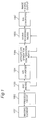
- Fig. 23 is a block diagram of the imaging apparatus disclosed in Japanese Patent Laid-Open Publication (tokkai) H4-340875 (1992-340875).
- this imaging apparatus comprises a lens 1; aperture mechanism 2; imaging element 3; a preamplifier 4 for amplifying the output from the imaging element 3 to an acceptable level; an integration circuit 5; an aperture control circuit 6; a process circuit 7 comprising a gamma correction circuit and white balance circuit; an automatic gain control (AGC) circuit 8; an integration circuit 9; an AGC control circuit 10 for generating a signal controlling the gain of the AGC circuit 8; an A/D converter 11 for analog-digital conversion of the image signal output from the AGC circuit 8; an image segmentation circuit 12 for segmenting the A/D-converted signal into plural segments; a multiplier 13 for calculating an evaluation value for the brightness of each signal segment in the segmented signal output by the image segmentation circuit 12; a frequency distribution calculator 14 for obtaining the frequency distribution of the signal segment brightness levels
- the imaging apparatus thus comprised operates as follows.
- the amount of light passing the lens 1 is limited by the aperture mechanism 2, converted to an electrical signal by the imaging element 3, and then amplified by the preamplifier 4.
- the output from the preamplifier 4 is integrated by the integration circuit 5, thus producing a dc signal corresponding to the output signal level from the preamplifier 4. This dc signal is supplied to the aperture control circuit 6.
- the aperture control circuit 6 compares the dc signal level input from the integration circuit 5 with a reference voltage to generate and output a control signal causing the aperture mechanism 2 to operate such that the output signal level of the preamplifier 4 is constant.
- the output from the preamplifier 4 is also supplied to the process circuit 7 for gamma correction and white balance control, and is then output to the AGC circuit 8.
- the output of the AGC circuit 8 is integrated by another integration circuit 9, thus producing a dc signal based on the output signal level of the AGC circuit 8. This dc signal is then compared by the AGC control circuit 10 with a reference voltage to generate an AGC control signal used to control the AGC circuit 8 to output at a constant output signal level.
- the output from the AGC circuit 8 is then converted to a digital signal by the A/D converter 11, and the resulting digital signal is segmented by the image segmentation circuit 12 into plural signal segments corresponding to specific image areas on screen.
- the multiplier 13 detects the average luminance distribution of the video signal in each image segment as the exposure value of each segment, and the frequency distribution calculator 14 obtains the luminance distribution in each segment.
- the microprocessor 16 determines the correlation between the image center and the other image segments, and defines as the main subject area the area with a correlation to the image center, and defines the other image areas as secondary subject areas. Based on the ratio of main subject areas to secondary subject areas, the microprocessor 16 then detects backlighting and strong normal lighting to control the image signal gain according to the backlighting-normal lighting ratio.
- the conventional technology described above detects the rate of the backlighting and strong normal lighting and controls the video signal gain according to this rate.
- the gain for low luminance level image areas is made higher than the gain for high luminance level areas in the image signal. It is therefore possible to provide gradation correction to dark image areas but at a cost of increasing the signal-to-noise (S/N) ratio in low luminance parts of the image signal.
- the object of the present invention is to resolve the aforementioned problems by providing an imaging apparatus whereby an output image with rich gradation can be obtained across the full range of subject lighting from normal to strongly backlit subjects without degrading the S/N ratio in low luminance image signal areas and while preventing loss or blurring of black and white definitions.
- an imaging apparatus comprises an imaging element outputting an image signal; an AGC circuit for controlling the gain of the image signal output from the imaging element; an AGC control means for controlling the output signal level of the AGC circuit to a constant level; a gradation compensation means for applying gradation compensation by varying the gain of each luminance level in the image signal output of the AGC circuit based on a gradation compensation coefficient; a feature quantity extraction means for extracting the feature quantities of the image from the image signal output of the AGC circuit; an image evaluation means for determining the amount of backlighting and strong normal lighting from the feature quantity extracted by the feature quantity extraction means, and outputting the degree of gradation compensation to be applied; and a gradation compensation suppression means for suppressing the degree of gradation compensation output from the image evaluation means and determining the gradation compensation coefficient according to the control signal from the AGC control means.
- An imaging apparatus comprises an imaging element outputting an image signal; a gradation compensation means for applying gradation compensation by varying the gain of each luminance level in the image signal output of the imaging element based on a gradation compensation coefficient; a signal processing circuit for applying contour enhancement and other signal processing to the image signal output of the gradation compensation means; a feature quantity extraction means for extracting the feature quantities of the image in the image signal output of the imaging element; an image evaluation means for determining the amount of backlighting and strong normal lighting from the feature quantity extracted by the feature quantity extraction means, and outputting the gradation compensation coefficient; and a contour signal gain control means for controlling the gain of the contour-enhanced signal output by the signal processing circuit based on the gradation compensation coefficient set by the image evaluation means.
- a further embodiment of an imaging apparatus comprises an imaging element outputting an image signal; a gradation compensation means for applying gradation compensation by varying the gain of each luminance level in the image signal output of the imaging element based on a gradation compensation coefficient; a signal processing circuit for applying contour enhancement and other signal processing to the image signal output of the gradation compensation means; a feature quantity extraction means for extracting the feature quantities of the image in the image signal output of the imaging element; an image evaluation means for determining the amount of backlighting and strong normal lighting from the feature quantity extracted by the feature quantity extraction means, and outputting the gradation compensation coefficient; and a noise reduction control means for controlling the noise suppression characteristic of the signal processing circuit based on the gradation compensation coefficient set by the image evaluation means.
- the imaging apparatus of the invention varies the gradation compensation coefficient set by the gradation compensation suppression means according to the AGC control signal of the AGC control means, and suppresses the gain of the gradation compensation means to output a gradation-compensated image signal.
- the imaging apparatus of the invention can thereby obtain a gradation compensated image of the input image without conspicuous noise.
- the imaging apparatus of the invention configured as described above controls the gradation compensation means according to the gradation compensation coefficient output by the image evaluation means to accomplish gradation compensation, and the contour signal gain control means controls the contour signal gain based on the gradation compensation coefficient of the image evaluation means so that the gain of the contour enhancement signal in low luminance image areas is reduced.
- the imaging apparatus of the invention can thereby obtain a gradation compensated image of the input image without conspicuous noise.
- the imaging apparatus of the invention alternatively configured as described above controls the gradation compensation means according to the gradation compensation coefficient output by the image evaluation means to accomplish gradation compensation, and controls the operating characteristics of the noise suppression control means according to the gradation compensation coefficient of the image evaluation means.
- This configuration of the invention can therefore also obtain a gradation compensated image of the input image without conspicuous noise.
- FIG. 1 is a block diagram of an imaging apparatus according to a first embodiment of the invention.
- the imaging apparatus of the first embodiment comprises an imaging element 1001, a process circuit 1002 comprising such as a gamma correction circuit and white balance circuit, an AGC means 1003, an A/D converter 1004 for A/D converting the image signal output of the AGC means 1003, an appropriate gradation compensation means 1005, a signal processing means 1006, and a D/A converter 1007 for D/A converting the image signal output of the signal processing means 1006.
- the appropriate gradation compensation means 1005 applies gradation compensation according to the input image.
- the signal processing means 1006 then applies a different signal processing operation to the gradation-compensated image signal output from the appropriate gradation compensation means 1005 based on the gain used by the appropriate gradation compensation means 1005 for the appropriate gradation compensation operation.
- the image signal generated by the imaging element 1001 is first processed by the process circuit 1002 for gamma correction, white balance control, and other operations as needed, and is then input to the AGC means 1003.
- the image signal output from the AGC means 1003 is then converted to a digital signal by the A/D converter 1004.
- the AGC means 1003 obtains the average of the total screen and the average of the screen center from the output signal of the A/D converter 1004, adds the averages, and obtains the integrated average.
- the obtained integrated average is thus normalized to the output level range of the AGC means 1003, and the output signal level of the AGC means 1003 is controlled to a constant level using the AGC control signal generated by comparing the normalized integrated average with a reference value.
- the image signal converted to a 256-level (0 - 255) digital signal by the A/D converter 1004 is then input to the appropriate gradation compensation means 1005.
- the appropriate gradation compensation means 1005 determines the degree of compensation of the gradation compensation characteristic to be applied based on the input image.
- the compensation gain is then set by suppressing the degree of compensation according to the AGC control signal of the AGC means 1003.
- the timing of the image signal is adjusted to the compensation gain by a delay circuit, multiplied with the compensation gain by a multiplier, and the gradation-compensated image signal is output.
- the signal processing means 1006 then applies a signal processing operation that differs according to the compensation gain of the appropriate gradation compensation means 1005 to the gradation-compensated image signal output by the appropriate gradation compensation means 1005.
- this different signal processing operation could control the detail gain of the detail compensation circuit inversely proportional to the compensation gain, or enhance the noise reduction of the noise reduction circuit according to the compensation gain.
- the D/A converter 1007 then converts the digital image signal to the analog image signal output therefrom.
- the imaging apparatus of the invention can link the operation of the AGC means 1003 and the appropriate gradation compensation means 1005 by means of the AGC control signal, and can link the appropriate gradation compensation means 1005 and signal processing means 1006 by means of the compensation gain.
- the imaging apparatus of the invention can produce an output image with rich gradation across the entire gradation range without gradation loss or conspicuous noise from subjects imaged in a lighting conditions ranging from backlit to normal lighting.
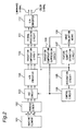
- FIG. 2 is a block diagram of an imaging apparatus according to a second embodiment of the invention.
- the imaging apparatus of the second embodiment comprises an imaging element 101, a process circuit 102 comprising such as a gamma correction circuit and white balance circuit, an AGC means 103, an A/D converter 104 for A/D converting the image signal output of the AGC means 103, an integration circuit 105, an AGC control circuit 106 for generating a signal controlling the gain of the AGC means 103, a feature quantity extraction circuit 107 for extracting the feature quantities of the image signal, an image evaluation means 108 for evaluating the backlighting and strong normal lighting of the input image, a gradation compensation suppression circuit 109 for setting the gradation compensation coefficient based on the output from the AGC control circuit 106 and the output from the image evaluation means 108, a gradation compensation circuit 110 for gradation compensating the output from the A/D converter 104 using the supplied gradation compensation coefficient, a signal processing circuit 111 for signal processing the gradation-compensated image signal input from the gradation compensation circuit 110, and a D/
- FIG. 3 shows the image in one field of the input image signal in a preferred embodiment of the invention.
- the effective screen area 201 shown in FIG. 3 is 320 pixels wide in the horizontal scanning direction and 240 pixels high in the vertical scanning direction.
- FIG. 4 is a sample luminance histogram showing the feature quantity extracted by the feature quantity extraction circuit 107 in the present embodiment of the invention.
- Curve a in FIG. 4 is the luminance histogram where the low luminance pixel count of pixels with a luminance value less than or equal to threshold value 1 is level b, the middle luminance pixel count of pixels with a luminance value between threshold value 1 and threshold value 2 is level c, and the high luminance pixel count of pixels with a luminance value greater than or equal to threshold value 2 is level d.
- FIG. 5A is a block diagram of the feature quantity extraction circuit 107 shown in FIG. 2. Shown in FIG. 5A are a comparator 401, low luminance pixel counter 402 for counting the low luminance pixels, middle luminance pixel counter 403 for counting the middle luminance pixels, and high luminance pixel counter 404 for counting the high luminance pixels.
- a comparator 401 for counting the low luminance pixels
- middle luminance pixel counter 403 for counting the middle luminance pixels
- high luminance pixel counter 404 for counting the high luminance pixels.
- FIG. 5B is a block diagram of the image evaluation means 108 shown in FIG. 2. Shown in FIG. 5B are the quantization table 501, output table 502, and filter 503.
- FIG. 6A is a block diagram of the integration circuit 105 and AGC control circuit 106 shown in FIG. 2.
- the integration circuit 105 comprises a full-screen averaging circuit 105a, center-weighted averaging circuit 105b, adder 105c, and normalization circuit 105d.
- the AGC control circuit 106 comprises a comparator 106a and AGC control signal output circuit 106b as also shown in FIG. 6A. Note that the comparator 106a compares the output from the normalization circuit 105d with a reference value, and outputs the resulting difference ⁇ E.
- FIG. 6B is a graph of the AGC control signal.
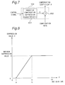
- FIG. 7 is a block diagram of the gradation compensation suppression means 109 in the present embodiment of the invention.
- the gradation compensation suppression circuit 109 comprises a gradation compensation suppression characteristic converter 601 and adder 602 as shown in the figure.
- FIG. 8 is a graph of the gradation compensation suppression characteristic based on the AGC control signal in the present embodiment of the invention.
- the pre-suppression gain is shown as point a in FIG. 8, and the highest suppressed gain is shown as point b.
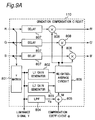
- FIG. 9A is a block diagram of the gradation compensation circuit shown in FIG. 2.
- the gradation compensation circuit 110 comprises a Y matrix circuit 801, L1 gain generator 802, L2 gain generator 803, average luminance detecting circuit (LPF) 804, adder 805, weighted-average circuit 806, delay circuits 807, and multipliers 808.
- LPF luminance detecting circuit
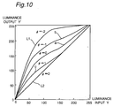
- FIG. 10 is a graph of the gradation compensation characteristic in the present embodiment of the invention.
- FIG. 11 is a graph of the gradation compensation characteristic and input/output characteristic in the present embodiment of the invention.
- the image signal captured by the imaging element 101 is first separated into the R, G, and B signal components which are then supplied to the process circuit 102.
- the process circuit 102 then processes the RGB signals for gamma correction, white balance control, and other operations as needed, and then outputs the signals to the AGC means 103
- the RGB image signal output from the AGC means 103 is then converted to a digital signal by the A/D converter 104.
- the A/D converter 104 outputs to the gradation compensation circuit 110, which then calculates the luminance signal Y by means of the Y matrix circuit 801 shown in FIG. 9A.
- This luminance signal Y is then supplied to the integration circuit 105 shown in FIG. 6A.
- the full-screen averaging circuit 105a of the integration circuit 105 calculates the average luminance of the overall screen (image) from the luminance signal Y.
- the center-weighted averaging circuit 105b calculates the average of the luminance signal Y in the middle of the screen, and then multiplies this average by a weight (for example, a multiplier of 2) to obtain the center-weighted average luminance of the image.
- the screen average and the center-weighted average luminance values are then added by the adder 105c, and this average sum signal is then normalized to the output level range of the AGC means 103 by the normalization circuit 105d, obtaining the integrated value that is then output to the AGC control circuit 106.
- the comparator 106a of the AGC control circuit 106 compares this integrated value with a reference value to obtain the difference signal ⁇ E.
- the AGC control signal output circuit 106b then generates the AGC control signal shown in FIG. 6B according to the difference signal ⁇ E, and outputs this AGC control signal from the AGC control circuit 106.
- This AGC control signal is used to maintain a constant output signal level from the AGC means 103.
- the AGC control signal is generated and output to increase the gain so that the integrated value and the reference value are equal.
- the output signal level of the AGC means 103 is thus controlled to a constant level.
- the AGC circuit of the invention is described in Japanese patent laid-open numbers (tokkai) 4-86074 and 4-94272, the content of which shall be considered part of the present invention.
- the A/D converter 104 converts the RGB signals from the AGC means 103 to 256-level digital signals comprising levels 0 - 255, and outputs the digitized RGB signals to the gradation compensation circuit 110.
- FIG. 3 One field of a typical image input signal is shown in FIG. 3.
- the feature quantity extraction circuit 107 obtains the luminance histogram shown in FIG. 4 by counting the low, middle, and high luminance pixels in one 320 x 240 pixel field of the effective screen area 201 shown in FIG. 3 to obtain the luminance distribution across one complete field of the effective screen area 201.
- This luminance histogram (FIG. 4bcd) shows that there are two luminance peaks with one in the low luminance range and one in the high luminance range. This makes it possible to deduce that the captured image contains a backlit subject.
- the image evaluation means 108 then sets the compensation rate of the gradation compensation characteristic used to compensate the input image based on the luminance histogram extracted by the feature quantity extraction circuit 107.
- the gradation compensation suppression circuit 109 then suppresses the compensation rate according to the AGC control signal of the AGC control circuit 106, and sets the gradation compensation coefficient.
- the gradation compensation circuit 110 then obtains the gradation-compensated luminance signal Y' from the luminance signal Y and gradation compensation coefficient, calculates the compensation gain (Y'/Y), adjusts the timing of the RGB signals to the compensation gain using the delay circuits 807, multiplies the delayed signals by the compensation gain (Y'/Y) using the multipliers 808, and thus outputs the gradation-compensated RGB signals R', G', and B'.
- the gradation compensation circuit 110 thus operates to convert the input luminance signal Y to a brighter luminance signal Y'.
- the input luminance signal Y and the output luminance signal Y' are equal, and the relationship between the two signals is expressed by a linear curve L2 with a slope of 45 degrees.
- the relationship between the two signals is expressed by curve L1.
- curve b is obtained
- the pre-suppression gradation compensation coefficient ⁇ (hereafter compensation rate ⁇ ) is output from the image evaluation means 108.
- compensation rate ⁇ As the AGC control signal F increases (variable from 0 - 12 dB as shown in FIG. 6B), suppression level S increases, compensation coefficient ⁇ is suppressed, and the output luminance signal converges to curve L2.
- the relationship between the AGC control signal F and the suppression level S is shown in FIG. 8 and expressed by equation 6.
- the input luminance signal Y is compared with threshold values 1 and 2 by the comparator 401. If the luminance signal Y is less than threshold value 1, a low luminance count signal is output. If luminance signal Y is between threshold values 1 and 2, a middle luminance count signal is output. If luminance signal Y is greater than threshold value 2, a high luminance count signal is output.
- the counters 402, 403, and 404 count these low, middle, and high luminance count signals as each pixel in one field of the effective screen area is evaluated, and then respectively output the low, middle, and high luminance pixel counts.
- Quantization tables addressed by the low, middle, and high luminance pixel counts supplied from the feature quantity extraction circuit 107 are stored in the quantization table 501 for normally illuminated subjects, backlit subjects, and dark subjects. Compensation rates for normally illuminated subjects, backlit subjects, and dark subjects are stored to the output table 502, which is addressed by quantized data input from the quantization table 501. These compensation rates have been determined from experience, and are described in detail in the previous specifications cited above. Thus, when the low, middle, and high luminance pixel counts supplied from the feature quantity extraction circuit 107 are input to the image evaluation means 108, the image evaluation means 108 selects one compensation rate for the input image. By thus using a two-stage table look-up in the image evaluation means 108, table size can be reduced. To maintain continuity between this compensation rate and the previous field or frame, a filtering process is applied by the filter 503 before outputting the compensation rate.
- the AGC control signal is input from the AGC control circuit 106 to the gradation compensation suppression circuit 109.
- the gradation compensation suppression characteristic converter 601 then converts the AGC control signal to a suppression value corresponding to the AGC control signal.
- the converted suppression value is then added to the compensation rate input from the image evaluation means 108 by the adder 602 to generate and output the compensation coefficient.
- the suppression value is low when the AGC control signal is low, and the suppression value increases as the AGC control signal level increases. This means that gradation compensation suppression increases as the AGC gain increases, and gradation compensation can be accomplished without conspicuous noise by linking gradation compensation to the automatic gain control process.
- the Y matrix circuit 801 calculates the luminance signal Y using the input RGB signals, and supplies the resulting luminance signal Y to the L1 gain generator 802 and L2 gain generator 803.
- the L1 gain generator 802 generates and outputs a first compensation gain (L1/Y) from the provided luminance signal Y and the curve L1 compensated by a first gradation compensation characteristic.
- the L2 gain generator 803 likewise outputs a second compensation gain (L2/Y).
- the average luminance detecting LPF 804 obtains the average luminance Ya from the luminance signal Y.
- the adder 805 then adds the average luminance Ya to the compensation coefficient ⁇ times 64 to obtain signal M.
- the weighted-average circuit 806 then applies equation 2' to obtain and output the weighted average compensation gain (Y'/Y) using the first compensation gain (L1/Y), second compensation gain (L2/Y), and signal M.
- (Y'/Y) ⁇ (L1/Y) ⁇ (255 - M) + (L2/Y) ⁇ M ⁇ /255
- the first compensation gain (L1/Y) is obtained from equation 3'
- the second compensation gain (L2/Y) is obtained from equation 4'.
- FIG. 10 is a graph of the gradation compensation characteristic in the present embodiment of the invention.
- curve L1 is the first gradation compensation characteristic and curve L2 is the second gradation compensation characteristic.
- curve a is obtained for the gradation compensation characteristic based on equation 2'.
- the compensation coefficient ⁇ is positive, the gradation compensation characteristic is curve c.
- the compensation coefficient ⁇ is negative, the gradation compensation characteristic is curve b.
- FIG. 11 is a graph of the gradation compensation characteristic and input/output characteristic in a preferred embodiment of the invention.
- the imaging apparatus of the invention can accomplish gradation compensation preserving contrast even when the compensation gain slope is low, and thereby achieve an output signal with rich gradation, by using gradation compensation characteristic a in FIG. 11 when the average luminance Ya obtained by the average luminance detecting LPF 804 is equal to the luminance signal Y of the target pixel, gradation compensation characteristic b when the average luminance Ya is less than the luminance signal Y of the target pixel, and gradation compensation characteristic c when the average luminance Ya is greater than the luminance signal Y of the target pixel.
- an imaging element 101 By thus comprising an imaging element 101, a process circuit 102 comprising such as a gamma correction circuit and white balance circuit, an AGC means 103, an A/D converter 104 for A/D converting the image signal output of the AGC means 103, an integration circuit 105, an AGC control circuit 106 for generating a signal controlling the gain of the AGC means 103, a feature quantity extraction circuit 107 for extracting the feature quantities of the image signal, an image evaluation means 108 for evaluating the backlighting and strong normal lighting of the input image, a gradation compensation suppression circuit 109 for setting the gradation compensation coefficient based on the output from the AGC control circuit 106 and the output from the image evaluation means 108, a gradation compensation circuit 110 for gradation compensating the output from the A/D converter 104 using the supplied gradation compensation coefficient, a signal processing circuit 111 for signal processing the gradation-compensated image signal input from the gradation compensation circuit 110, and a D/A converter 112 for
- the gradation compensation circuit 110 can generate the compensation gain levels according to the compensation coefficient. It is therefore not necessary to provide extra ROM for storing plural gradation compensation characteristics, and the circuit scale can be greatly reduced.
- gradation compensation characteristics can be generated for normal and backlit subjects by changing the compensation coefficient ⁇ , an output image with rich gradation across the entire luminance range can be achieved with good color balance using subjects ranging from backlit to normally illuminated subjects without gradation loss.
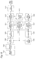
- FIG. 12 is a block diagram of an imaging apparatus according to a third embodiment of the invention.
- the imaging apparatus of the third embodiment comprises an imaging element 1101, a process circuit 1102 comprising such as a gamma correction circuit and white balance circuit, an A/D converter 1103 for A/D converting the image signal output of the process circuit 1102, a feature quantity extraction circuit 1104 for extracting the feature quantities of the image signal, an image evaluation means 1105 for evaluating the backlighting and strong normal lighting of the input image, a DTL gain control means 1106 for determining the DTL gain based on the image evaluation result, a gradation compensation circuit 1107 for gradation compensating the output from the A/D converter 1103 using the gradation compensation coefficient, a signal processing circuit 1108 for applying such as detail compensation signal processing to the gradation-compensated image signal input from the gradation compensation circuit 1107, and a D/A converter 1109 for D/A converting the image signal output of the signal processing circuit 1108.
- a process circuit 1102 comprising such as a gamma correction circuit and white balance circuit
- an A/D converter 1103 for
- FIG. 13 is a block diagram of the signal processing circuit 1108 shown in FIG. 12 according to this third embodiment.
- the signal processing circuit 1108 comprises a vertical detail circuit 1201, horizontal detail circuit 1202, adder 1203, multiplier 1204, delay circuit 1205, and adder 1206
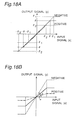
- FIG. 14 is a graph of detail control based on the luminance signal Y in the third embodiment of the invention.
- FIG. 9B is a block diagram of the gradation compensation circuit 1107 in the third embodiment of the invention.
- the gradation compensation circuit 1107 comprises a L1 gain generator 802, L2 gain generator 803, average luminance detecting circuit (LPF) 804, adder 805, weighted-average circuit 806, delay circuit 807, and multiplier 808.
- LPF average luminance detecting circuit
- the operation of an imaging apparatus is described below.
- the image signal generated by the imaging element 1101 is first processed by the process circuit 1102 for gamma correction, white balance control, and other operations as needed, and is then input to the A/D converter 1103.
- the image signal from the process circuit 1102 is then converted to a digital signal by the A/D converter 1103.
- the image signal converted to a 256-level (0 - 255) digital signal by the A/D converter 1103 is then input to the gradation compensation circuit 1107 and the feature quantity extraction circuit 1104.
- the operations of the feature quantity extraction circuit 1104 and the image evaluation means 1105 are identical to the operation of those means in the second embodiment above. Specifically, the feature quantity extraction circuit 1104 obtains the luminance histogram of the image signal, and the image evaluation means 1105 sets the compensation coefficient of the gradation compensation characteristic to be used for compensating the image signal based on the luminance histogram extracted by the feature quantity extraction circuit 1104.
- the gradation compensation circuit 1107 then obtains the luminance signal Y' after compensation from the luminance signal Y and compensation coefficient, calculates the compensation gain (Y'/Y), and adjusts the timing of the input image signal and the compensation gain of the delay circuit 807.
- the multiplier 808 then multiplies the delayed image signal with the compensation gain (Y'/Y) to output the gradation-compensated output image signal with rich gradation across the entire luminance range.
- the DTL gain control means 1106 uses the compensation coefficient set by the image evaluation means 1105 to reduce the detail gain in low luminance areas, and outputs a detail gain level corresponding to the luminance signal Y.
- the gradation-compensated image signal is also input from the gradation compensation circuit 1107 to the signal processing circuit 1108, which applies detail compensation signal processing based on the detail gain level set by the DTL gain control means 1106.
- the D/A converter 1109 then re-converts the image signal to an analog output image signal.
- DTL gain control means 1106 and signal processing circuit 1108 of this embodiment are described in detail below with reference to FIG. 13 and FIG. 14.
- the DTL gain control means 1106 has detail gain characteristics corresponding to the luminance signal Y as shown in FIG. 14. Specifically, these characteristics reduce the detail gain in low luminance areas and increase the detail gain in high luminance areas. This is to reduce deterioration of the S/N ratio in low luminance areas, and to compensate for loss of detail resulting from gamma correction in high luminance areas.
- the gradation compensation circuit 1107 of the present embodiment accomplished gradation compensation by using a higher gain level in low luminance areas than in high luminance areas, thus resulting in S/N ratio degradation in low luminance areas.
- the compensation coefficient ⁇ 2
- edge components in dark areas will be emphasized using the detail gain G of the low luminance areas as a reference.
- the compensation coefficient ⁇ 0
- the subject is backlit and the image contains both dark and light areas.
- Gradation compensation by the gradation compensation circuit 1107 thus works to increase gradation in dark areas, but this also enhances noise.
- the detail gain G is reduced for dark, low luminance areas, thus suppressing edge enhancement and preventing noise from being emphasized.
- FIG. 13 is a block diagram of the signal processing circuit 1108.
- the input image signal is supplied to the delay circuit 1205 as well as the vertical detail circuit 1201 and the horizontal detail circuit 1202.
- the vertical detail circuit 1201 applies a high pass filtering process in the vertical direction to output a vertical detail signal
- the horizontal detail circuit 1202 applies a high pass filtering process in the horizontal direction to output a horizontal detail signal.
- the horizontal and vertical detail signals are then combined by the adder 1203 to produce the detail signal.
- This detail signal is then multiplied by the multiplier 1204 with the detail gain input from the DTL gain control means 1106 to adjust the detail level.
- the detail signal is then added by the adder 1206 with the input image signal delayed for timing control by the delay circuit 1205 to output the detail-compensated image signal.
- an imaging element 1101 By thus comprising an imaging element 1101, a process circuit 1102 comprising such as a gamma correction circuit and white balance circuit, an A/D converter 1103 for A/D converting the image signal output of the process circuit 1102, a feature quantity extraction circuit 1104 for extracting the feature quantities of the image signal, an image evaluation means 1105 for evaluating the backlighting and strong normal lighting of the input image, a DTL gain control means 1106 for determining the DTL gain based on the image evaluation result, a gradation compensation circuit 1107 for gradation compensating the output from the A/D converter 1103 using the gradation compensation coefficient, a signal processing circuit 1108 for applying such as detail compensation signal processing to the gradation-compensated image signal input from the gradation compensation circuit 1107, and a D/A converter 1109 for D/A converting the image signal output of the signal processing circuit 1108, the imaging apparatus of the present embodiment can generate the compensation gain levels according to the compensation coefficient. It is therefore not necessary to provide extra ROM for storing plural
- gradation compensation characteristics can be generated for normal and backlit subjects by changing the compensation coefficient ⁇ , an output image with rich gradation across the entire luminance range can be achieved with good color balance using subjects ranging from backlit to normally illuminated subjects without gradation loss.
- the imaging apparatus of the invention can accomplish gradation compensation preserving contrast and achieving rich gradation in the output signal even when the slope of compensation gain is low by appropriately varying the gradation compensation characteristic on a pixel unit level based on the average luminance value Ya for gradation compensation.
- FIG. 15 is a block diagram of an imaging apparatus according to a fourth embodiment of the invention.
- the imaging apparatus of the fourth embodiment comprises an imaging element 1401, a process circuit 1402 comprising such as a gamma correction circuit and white balance circuit, an AGC means 1403, an A/D converter 1404 for A/D converting the image signal output of the AGC means 1403, an integration circuit 1405, an AGC control circuit 1406 for generating a signal controlling the gain of the AGC means 1403, a feature quantity extraction circuit 1407 for extracting the feature quantities of the image signal, an image evaluation means 1408 for evaluating the backlighting and strong normal lighting of the input image, a gradation compensation suppression circuit 1409 for setting the gradation compensation coefficient based on the output from the AGC control circuit 1406 and the output from the image evaluation means 1408, a DTL gain control means 1410 for determining the DTL gain based on the compensation coefficient set by the gradation compensation suppression circuit 1409, a gradation compensation circuit 1411 for gradation compensating the output from the A/D converter 1404 using the supplied gradation compensation coefficient, a signal processing circuit
- the image signal generated by the imaging element 1401 is first processed by the process circuit 1402 for gamma correction, white balance control, and other operations as needed, and is then input to the AGC means 1403.
- the image signal from the AGC means 1403 is then converted to a digital signal by the A/D converter 1404.
- the output signal of the A/D converter 1404 is input to the integration circuit 1405, which is constructed identically to the integration circuit 105 shown in FIG. 6A.
- the full-screen averaging circuit 105a of the integration circuit 105 calculates the average luminance of the overall screen (image) from the output signal of the A/D converter 1404.
- the center-weighted averaging circuit 105b calculates the average in the middle of the screen, and then multiplies this average by a weight (for example, a multiplier of 2) to obtain the center-weighted average of the image.
- the screen average and the center-weighted average are then added by the adder 105c, and this average sum signal is then normalized to the output level range of the AGC means 1403 by the normalization circuit 105d, obtaining the integrated value that is then output to the AGC control circuit 1406.
- the AGC control circuit 1406 is also constructed identically to the AGC control circuit 106 shown in FIG. 6A.
- the comparator 106a of the AGC control circuit 1406 compares this integrated value with a reference value, and the AGC control signal output circuit 106b then generates the AGC control signal whereby the output signal level of the AGC means 1403 is controlled to a constant level.
- the AGC control signal is generated and output to increase the gain so that the integrated value and the reference value are equal.
- the output signal level of the AGC means 1403 is thus controlled to a constant level.
- the A/D converter 1404 converts the image signal from the AGC means 1403 to 256-level digital signals comprising levels 0 - 255, and outputs the digitized image signal to the integration circuit 1405, the feature quantity extraction circuit 1407, and the gradation compensation circuit 1411.
- the operations of the feature quantity extraction circuit 1407 and the image evaluation means 1408 are identical to the operation of those means in the first and third embodiments above. Specifically, the feature quantity extraction circuit 1407 obtains the luminance histogram of the image signal, and the image evaluation means 1408 sets the compensation coefficient of the gradation compensation characteristic to be used for compensating the image signal based on the luminance histogram.
- the gradation compensation suppression circuit 1409 then suppresses the compensation rate according to the AGC control signal of the AGC control circuit 1406, and sets the gradation compensation coefficient.
- the gradation compensation circuit 1411 then obtains the gradation-compensated luminance signal Y' from the luminance signal Y and gradation compensation coefficient, calculates the compensation gain (Y'/Y), adjusts the timing of the input image signal to the compensation gain using the delay circuits 807, multiplies the delayed signals by the compensation gain (Y'/Y) using the multipliers 808, and thus outputs a gradation-compensated image signal with good color balance and rich overall gradation.
- gradation compensation can be accomplished without conspicuous noise in low luminance areas.
- the DTL gain control means 1410 uses the compensation coefficient ⁇ set by the gradation compensation suppression circuit 1409 to control the gain to reduce the detail gain in low luminance areas, and outputs a detail gain level corresponding to the luminance signal Y.
- the gradation-compensated image signal is also input from the gradation compensation circuit 1411 to the signal processing circuit 1412, which applies detail compensation signal processing based on the detail gain level set by the DTL gain control means 1410.
- the D/A converter 1413 then re-converts the image signal to an analog output image signal.
- a process circuit 1402 comprising such as a gamma correction circuit and white balance circuit, an AGC means 1403, an A/D converter 1404 for A/D converting the image signal output of the AGC means 1403, an integration circuit 1405, an AGC control circuit 1406 for generating a signal controlling the gain of the AGC means 1403, a feature quantity extraction circuit 1407 for extracting the feature quantities of the image signal, an image evaluation means 1408 for evaluating the backlighting and strong normal lighting of the input image, a gradation compensation suppression circuit 1409 for setting the gradation compensation coefficient based on the output from the AGC control circuit 1406 and the output from the image evaluation means 1408, a DTL gain control means 1410 for determining the DTL gain based on the compensation coefficient set by the gradation compensation suppression circuit 1409, a gradation compensation circuit 1411 for gradation compensating the output from the A/D converter 1404 using the supplied gradation compensation coefficient, a signal processing circuit 1412 for signal processing the gradation-
- gradation compensation characteristics can be generated for normal and backlit subjects by changing the compensation coefficient, an output image with rich gradation across the entire luminance range can be achieved with good color balance using subjects ranging from backlit to normally illuminated subjects without gradation loss.
- gradation compensation is regulated by an AGC control signal and the detail gain in low luminance areas is controlled according to the compensation coefficient, gradation compensation without conspicuous noise is possible.
- the imaging apparatus of the invention can accomplish gradation compensation preserving contrast and achieving rich gradation in the output signal even when the slope of compensation gain is low by appropriately varying the gradation compensation characteristic on a pixel unit level based on the average luminance Ya value for gradation compensation.
- luminance signal Y and RGB signals have been used by way of example for the input image signals in the preceding embodiments, the same effects can be achieved by using in place of the luminance signal Y and RGB signals a luminance signal and color difference signals, a composite signal, or a signal mixing a chrominance signal with the luminance signal.
- the gradation compensation means of the above embodiments multiply a compensation gain coefficient with each of the input image signals to effect gradation compensation.
- the same effect can be achieved by using the compensation value (Y' - Y) in place of the compensation gain coefficient (Y'/Y) and adding this compensation value to the input image signals.
- the feature quantity extraction circuits of the above embodiments have been described outputting pixel counts for three luminance levels.
- the threshold values demarcating these luminance levels shall not be limited to those described above, however. Other threshold values can specifically be used, and the number of luminance levels shall also not be limited to three.
- the above embodiments have been described with the feature quantity extraction circuit counting the pixels in an effective screen area measuring 240 scan lines high by 320 pixels per horizontal scan line.
- the number of pixels counted shall not be so limited, however, and the number of signal bits representing one pixel can be any number of bits whereby the features of the input image can be known.
- the compensation coefficient setting circuit evaluating the input image using a luminance histogram as the feature quantity
- the invention shall not be so limited and other feature quantities can be used in place of the luminance histogram.
- histograms of the combined RGB signal or any one of the RGB signals can be used, or the effective screen area of the image data can be segmented into blocks, and the luminance signal, RGB signals, or maximum, average, or minimum color difference signals of each block can be used for the corresponding feature quantity.
- the invention shall not be limited to these feature quantities, and any feature quantity whereby the image can be segmented into identifiable classes can be used.
- the compensation coefficient setting circuit of the invention shall also not be limited to any single type or method, and can be achieved using a neural network, fuzzy logic control, template matching, or other method whereby the image can be evaluated and the gradation compensation characteristics determined.
- the imaging apparatus of the invention can generate compensation gain levels according to the compensation coefficient. It is therefore not necessary to provide extra ROM for storing plural gradation compensation characteristics, and the circuit scale can be greatly reduced.
- gradation compensation characteristics can be generated for normal and backlit subjects by changing the compensation coefficient, an output image with rich gradation across the entire image range can be achieved with good color balance using subjects ranging from backlit to normally illuminated subjects without gradation loss.
- gradation compensation is regulated by an AGC control signal and the detail gain in low luminance areas is controlled according to the compensation coefficient, gradation compensation without conspicuous noise is possible.
- the imaging apparatus of the invention can accomplish gradation compensation preserving contrast and achieving rich gradation in the output signal even when the slope of compensation gain is low by appropriately varying the gradation compensation characteristic on a pixel unit level based on the average luminance Ya value for gradation compensation.
- FIG. 16 is a block diagram of an imaging apparatus according to a fifth embodiment of the invention.
- the imaging apparatus of the fifth embodiment comprises an imaging element 1601, a process circuit 1602 comprising such as a gamma correction circuit and white balance circuit, an A/D converter 1603 for A/D converting the image signal output of the process circuit 1602, a feature quantity extraction circuit 1604 for extracting the feature quantities of the image signal, an image evaluation means 1605 for evaluating the backlighting and strong normal lighting of the input image, a noise reduction control means 1606 for controlling the noise suppression characteristic based on the image evaluation result, a gradation compensation circuit 1607 for gradation compensating the output from the A/D converter 1603 using the gradation compensation coefficient, a signal processing circuit 1608 for applying such as noise reduction signal processing to the gradation-compensated image signal input from the gradation compensation circuit 1607, and a D/A converter 1609 for D/A converting the image signal output of the signal processing circuit 1608.
- a process circuit 1602 comprising such as a gamma correction circuit and white balance circuit
- an A/D converter 1603 for A/
- the imaging apparatus of the fifth embodiment thus comprised operates as follows.
- the imaging element 1601, process circuit 1602, A/D converter 1603, feature quantity extraction circuit 1604, image evaluation means 1605, and gradation compensation circuit 1607 operate identically to the corresponding imaging element 1101, process circuit 1102, A/D converter 1103, feature quantity extraction circuit 1104, image evaluation means 1105, and gradation compensation circuit 1107 of the third embodiment above. More specifically, the image evaluation means 1605 evaluates the image captured by the imaging element 1601 for backlighting and strong normal lighting to output a compensation coefficient, and the gradation compensation circuit 1607 then applies gradation compensation based on that compensation coefficient.
- the noise reduction control means 1606 When the compensation coefficient output by the image evaluation means 1605 is low, the noise reduction control means 1606 outputs a noise suppression characteristic signal so that the noise suppression characteristic of the signal processing circuit 1608 is increased. The signal processing circuit 1608 then applies noise reduction signal processing according to this suppression characteristic.
- the D/A converter 1609 then re-converts the output of the signal processing circuit 1608 to an analog image signal output.
- FIG. 17 is a block diagram of the signal processing circuit 1608 and noise reduction control circuit 1606 shown in FIG. 16 according to the fifth embodiment of the invention. Shown in FIG. 17 are a delay means 1701, a non-linear processor 1702, a non-linear characteristic selector (noise reduction controller IN THE FIGURES) 1703, subtracters 1704 and 1705, an image signal input terminal 1706, an image signal output terminal 1707, and a gradation compensation coefficient input terminal 1708 connected to the image evaluation means 1605.
- a delay means 1701 Shown in FIG. 17 are a delay means 1701, a non-linear processor 1702, a non-linear characteristic selector (noise reduction controller IN THE FIGURES) 1703, subtracters 1704 and 1705, an image signal input terminal 1706, an image signal output terminal 1707, and a gradation compensation coefficient input terminal 1708 connected to the image evaluation means 1605.
- the delay means 1701 delays the image signal Y1 ((a) in FIG. 18C) input from the image signal input terminal 1706 one line, and outputs delayed signal Y2 ((b) in FIG. 18C).
- the subtracter 1704 obtains and outputs the difference signal x ((c) in FIG. 18C) from the current image signal Y1 and the image signal Y2 delayed from the previous line.
- the non-linear characteristic selector (noise reduction controller) 1703 sets the input/output characteristic of the non-linear processor 1702 according to the gradation compensation coefficient input from the gradation compensation coefficient input terminal 1708. Based on the input/output characteristic set by the noise reduction controller 1703, the non-linear processor 1702 processes the difference signal x from the subtracter 1704 and outputs signal y ((d) in FIG. 18C). The subtracter 1705 obtains and outputs the difference Y3 ((e) in FIG. 18C) between signal y and the image signal Y1 from the image signal input terminal 1706.
- FIG. 18A is an input/output characteristics graph of the non-linear processor 1702 in the fifth embodiment of the invention.
- the input signal x to the non-linear processor 1702 is plotted on the horizontal axis
- the output signal y of the non-linear processor 1702 is plotted on the vertical axis in FIG. 18A.
- the input/output characteristic of the non-linear processor 1702 is defined by equation 7.
- the characteristic of equation 7 is set by the noise reduction controller 1703.
- the noise reduction controller 1703 determines the value of ⁇ using equation 8 based on the value of the gradation compensation coefficient.
- the input/output characteristic of the non-linear processor 1702 varies according to equation 8 as shown in FIG. 18A according to the present embodiment.
- the noise reduction characteristic is enhanced and gradation compensation in which noise is not conspicuous can be accomplished in images for which the gradation compensation coefficient is negative and the gain of the gradation compensation circuit 1607 is high.
- the delay means 1701 of the present embodiment is a line memory delaying the input signal Y1 one line
- the delay means 1701 can alternatively comprise a flip-flop delaying the image signal Y1 one clock or longer, or a field memory delaying the input signal one field or more.
- the signal processing circuit 1608 of the present embodiment is a feed-forward noise reduction circuit in which a delay means 1701 delays the input signal Y1, but it can also be achieved as a feedback-type noise reduction circuit in which the delay means 1701 delays the output signal Y3.
- FIG. 19 is a block diagram of a noise reduction control means 1606 and signal processing circuit 1608 comprising a feedback-type noise reduction circuit using the component elements (shown in FIG. 17) of the signal processing circuit 1608 of the embodiment described above.
- the configuration shown in FIG. 19, however, can achieve a greater noise reduction effect than the above feed-forward design even using a delay means operating at the same delay time.
- FIG. 20 is a block diagram of a noise reduction control means 1606 and signal processing circuit 1608 comprising the noise reduction circuit shown in FIG. 19 and the noise reduction circuit shown in FIG. 17 connected in series.
- the line memory 2241, vertical non-linear processor 2242, vertical noise reduction control means 2243, and subtracters 2247 and 2248 form a circuit removing the vertical noise component from the image by using a line memory 2241 delaying the signal one line for the delay means 2101 of the signal processing circuit shown in FIG. 19.
- the flip-flop 2244, horizontal non-linear processor 2245, noise reduction control means 2246, and subtracters 2249 and 2250 form a circuit removing the horizontal noise component from the image by using a flip-flop 2244 delaying the signal one clock period for the delay means 1701 of the signal processing circuit shown in FIG. 17.
- the signal processing circuit 1608 of this embodiment comprises a noise reduction circuit that uses the difference signal between the input signal Y1 and the output signal Y2 of the delay means 1701. It may be alternatively comprised as a noise reduction circuit that uses the band-divided difference signal of Y2 and Y1.
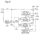
- FIG. 21 is a block diagram of this type of signal processing circuit 1608 and noise reduction control means 1606.
- this configuration comprises a delay means 2321, band divider 2322, first non-linear processor 2323, second non-linear processor 2324, first noise reduction control means 2325, second noise reduction control means 2326, an adder 2327, subtracters 2328 and 2329, an image signal input terminal 2330, image signal output terminal 2331, and gradation compensation coefficient input terminal 2332.
- the delay means 2321 delays the input image signal Y1 one line, and outputs delayed signal Y2.
- the subtracter 2328 subtracts the delayed signal Y2 from the image signal Y1, and outputs difference signal x.
- the band divider 2322 then divides the difference signal x into low frequency component x1 and high frequency component x2.
- the first non-linear processor 2323 and the second non-linear processor 2324 apply different signal processing operations (input/output characteristics having different ⁇ values in FIG. 18) to the respective low and high frequency components x1 and x2, and output y1 and y2.
- the first noise reduction control means 2325 determines the value ⁇ in the input/output characteristic of the first non-linear processor 2323 according to the value of the gradation compensation coefficient.
- the second noise reduction control means 2326 likewise determines the value ⁇ in the input/output characteristic of the second non-linear processor 2324 according to the level of the input signal Y1.
- the adder 2327 then adds the y1 and y2 output signals of the first and second non-linear processor 2323 and 2324, and outputs signal y.
- the subtracter 2329 then subtracts signal y from the input signal Y1, and outputs signal Y3.
- This operation thus achieves a different noise reduction effect in the high and low frequency components of the difference signal x.
- the value of ⁇ in the input/output characteristic of the second non-linear processor 2324 is greater than the value of ⁇ in the input/output characteristic of the first non-linear processor 2323, a stronger noise reduction effect can be achieved in the high frequency component of the difference signal than in the low frequency component.
- the signal processing circuit 1608 and noise reduction control means 1606 of this configuration can be configured as a feedback-type noise reduction circuit using band division as shown in FIG. 22. Note, also, that the configuration shown in FIG. 22 can achieve a greater noise reduction effect than the feed-forward design described above even using a delay means operating at the same delay time.
Landscapes
- Engineering & Computer Science (AREA)
- Multimedia (AREA)
- Signal Processing (AREA)
- Studio Devices (AREA)
- Color Television Image Signal Generators (AREA)
- Processing Of Color Television Signals (AREA)
- Picture Signal Circuits (AREA)
Applications Claiming Priority (5)
| Application Number | Priority Date | Filing Date | Title |
|---|---|---|---|
| JP23673294A JP3531230B2 (ja) | 1994-09-30 | 1994-09-30 | ノイズ低減回路 |
| JP236732/94 | 1994-09-30 | ||
| JP24277494A JP3298330B2 (ja) | 1994-10-06 | 1994-10-06 | 撮像装置 |
| JP242774/94 | 1994-10-06 | ||
| PCT/JP1995/001990 WO1996010886A1 (fr) | 1994-09-30 | 1995-09-29 | Dispositif de prise de vues |
Publications (3)
| Publication Number | Publication Date |
|---|---|
| EP0784399A1 true EP0784399A1 (fr) | 1997-07-16 |
| EP0784399A4 EP0784399A4 (fr) | 1999-10-06 |
| EP0784399B1 EP0784399B1 (fr) | 2006-04-12 |
Family
ID=26532819
Family Applications (1)
| Application Number | Title | Priority Date | Filing Date |
|---|---|---|---|
| EP95932941A Expired - Lifetime EP0784399B1 (fr) | 1994-09-30 | 1995-09-29 | Dispositif de prise de vues |
Country Status (4)
| Country | Link |
|---|---|
| US (1) | US6040860A (fr) |
| EP (1) | EP0784399B1 (fr) |
| DE (1) | DE69534929T2 (fr) |
| WO (1) | WO1996010886A1 (fr) |
Cited By (8)
| Publication number | Priority date | Publication date | Assignee | Title |
|---|---|---|---|---|
| EP0866608A2 (fr) * | 1997-03-18 | 1998-09-23 | Matsushita Electric Industrial Co., Ltd. | Méthode pour corriger la gradation de luminance dans un appareil de prise d'images |
| EP0871329A2 (fr) * | 1997-03-14 | 1998-10-14 | Matsushita Electric Industrial Co., Ltd. | Capteur d'images |
| EP1117088A1 (fr) * | 1999-06-07 | 2001-07-18 | Seiko Epson Corporation | Appareil et procede d'affichage d'image, et dispositif et procede de traitement d'image |
| EP1237360A1 (fr) * | 1999-11-30 | 2002-09-04 | Sharp Kabushiki Kaisha | Dispositif de correction de contour |
| WO2004068850A1 (fr) * | 2003-01-17 | 2004-08-12 | Robert Bosch Gmbh | Procede de reglage d'un capteur d'images |
| NL1028642C2 (nl) * | 2004-05-21 | 2006-05-09 | Samsung Electronics Co Ltd | Inrichting voor gammacorrectie en werkwijze in staat om versterking van ruis te voorkomen. |
| EP1786214A2 (fr) * | 2005-11-14 | 2007-05-16 | Pioneer Corporation | Dispositif d'affichage, circuit de traitement de signaux, programme et procédé d'affichage |
| CN100428330C (zh) * | 2004-02-24 | 2008-10-22 | 株式会社日立制作所 | 图像显示方法及其装置 |
Families Citing this family (45)
| Publication number | Priority date | Publication date | Assignee | Title |
|---|---|---|---|---|
| US6215529B1 (en) * | 1997-03-06 | 2001-04-10 | Matsushita Electric Industrial Co. Ltd. | Gamma compensation apparatus |
| US6906745B1 (en) * | 1998-04-23 | 2005-06-14 | Micron Technology, Inc. | Digital exposure circuit for an image sensor |
| JP3969836B2 (ja) * | 1998-04-24 | 2007-09-05 | キヤノン株式会社 | 信号処理装置および撮像用信号処理方法 |
| US6825884B1 (en) * | 1998-12-03 | 2004-11-30 | Olympus Corporation | Imaging processing apparatus for generating a wide dynamic range image |
| JP4255553B2 (ja) * | 1999-02-04 | 2009-04-15 | パナソニック株式会社 | 撮像装置 |
| JP3714657B2 (ja) * | 1999-05-12 | 2005-11-09 | パイオニア株式会社 | 階調補正装置 |
| JP4482956B2 (ja) * | 1999-06-03 | 2010-06-16 | 株式会社ニコン | 画像補正装置及び画像補正プログラムを記録した記録媒体。 |
| US7092569B1 (en) * | 1999-07-29 | 2006-08-15 | Fuji Photo Film Co., Ltd. | Method and device for extracting specified image subjects |
| CA2390200A1 (fr) * | 1999-11-03 | 2001-05-10 | Charles W. K. Gritton | Systeme de traitement vocal integre pour reseaux a commutation par paquets |
| US6567124B1 (en) * | 1999-12-01 | 2003-05-20 | Ball Aerospace & Technologies Corp. | Electronic image processing technique for achieving enhanced image detail |
| JP3757747B2 (ja) * | 2000-04-03 | 2006-03-22 | 株式会社ニコン | 電子カメラ、画像処理プログラムを記録した記録媒体、および画像処理方法 |
| US6735547B1 (en) * | 2000-10-06 | 2004-05-11 | Evangelos A. Yfantis | Method and apparatus for determining the size and shape of a foot |
| US7176962B2 (en) * | 2001-03-01 | 2007-02-13 | Nikon Corporation | Digital camera and digital processing system for correcting motion blur using spatial frequency |
| US6900888B2 (en) * | 2001-09-13 | 2005-05-31 | Hitachi High-Technologies Corporation | Method and apparatus for inspecting a pattern formed on a substrate |
| JP3992177B2 (ja) * | 2001-11-29 | 2007-10-17 | 株式会社リコー | 画像処理装置、画像処理方法及びコンピュータ・プログラム |
| JP2004023605A (ja) * | 2002-06-19 | 2004-01-22 | Sony Corp | 画像処理装置、カメラ装置、及びその自動露光制御方法 |
| US6853806B2 (en) * | 2002-09-13 | 2005-02-08 | Olympus Optical Co., Ltd. | Camera with an exposure control function |
| JP4167097B2 (ja) * | 2003-03-17 | 2008-10-15 | 株式会社沖データ | 画像処理方法および画像処理装置 |
| JP2004318609A (ja) * | 2003-04-17 | 2004-11-11 | Sanyo Electric Co Ltd | 画像処理装置、画像処理方法及び画像処理プログラム |
| JP4200890B2 (ja) * | 2003-12-10 | 2008-12-24 | 株式会社日立製作所 | 映像信号処理装置及びそれを用いたテレビジョン受信機並びに映像信号処理方法 |
| JP4286124B2 (ja) * | 2003-12-22 | 2009-06-24 | 三洋電機株式会社 | 画像信号処理装置 |
| KR100613912B1 (ko) * | 2004-01-26 | 2006-08-17 | 엘지전자 주식회사 | 영상 처리 장치 및 그 방법 |
| JP4250595B2 (ja) * | 2004-02-16 | 2009-04-08 | キヤノン株式会社 | 信号処理方法及び信号処理回路 |
| KR100609155B1 (ko) * | 2004-03-22 | 2006-08-02 | 엘지전자 주식회사 | 영상 처리 장치 및 이를 이용한 역광 보정 방법 |
| KR100610478B1 (ko) * | 2004-05-06 | 2006-08-08 | 매그나칩 반도체 유한회사 | 이미지센서 및 그의 디지털 이득 보상 방법 |
| EP1781043B1 (fr) * | 2004-07-07 | 2013-01-23 | Nikon Corporation | Processeur d'image et produit de programme informatique |
| KR100600991B1 (ko) * | 2004-12-15 | 2006-07-13 | 주식회사 팬택앤큐리텔 | 플래시 자동 제어 기능을 가지는 무선통신 단말기 및 그방법 |
| JP4622629B2 (ja) * | 2005-03-31 | 2011-02-02 | 株式会社ニコン | 撮像装置 |
| JP2006333202A (ja) * | 2005-05-27 | 2006-12-07 | Matsushita Electric Ind Co Ltd | 映像信号処理装置、および映像信号処理方法 |
| JP4831067B2 (ja) * | 2005-06-20 | 2011-12-07 | 株式会社ニコン | 画像処理装置、画像処理方法、画像処理プログラム製品、および撮像装置 |
| JP4419933B2 (ja) * | 2005-08-26 | 2010-02-24 | ソニー株式会社 | 画像処理装置、画像表示装置および画像処理方法 |
| US20070153117A1 (en) * | 2005-12-30 | 2007-07-05 | Yen-Yu Lin | Apparatus and method for adjusting display-related setting of an electronic device |
| JP5103984B2 (ja) * | 2007-03-29 | 2012-12-19 | 株式会社ニコン | 画像処理装置、撮像装置、および画像処理プログラム |
| US20080255840A1 (en) * | 2007-04-16 | 2008-10-16 | Microsoft Corporation | Video Nametags |
| US8526632B2 (en) * | 2007-06-28 | 2013-09-03 | Microsoft Corporation | Microphone array for a camera speakerphone |
| US8165416B2 (en) * | 2007-06-29 | 2012-04-24 | Microsoft Corporation | Automatic gain and exposure control using region of interest detection |
| US8330787B2 (en) | 2007-06-29 | 2012-12-11 | Microsoft Corporation | Capture device movement compensation for speaker indexing |
| JP4835525B2 (ja) * | 2007-07-04 | 2011-12-14 | ソニー株式会社 | 画像処理装置、画像処理方法及びプログラム |
| JP4524711B2 (ja) * | 2008-08-04 | 2010-08-18 | ソニー株式会社 | ビデオ信号処理装置、ビデオ信号処理方法、プログラム |
| KR102051538B1 (ko) * | 2013-09-13 | 2020-01-08 | 에스케이하이닉스 주식회사 | 신호 처리 장치 및 그의 동작 방법 |
| CN104021773B (zh) * | 2014-05-30 | 2015-09-09 | 京东方科技集团股份有限公司 | 一种显示器件的亮度补偿方法、亮度补偿装置及显示器件 |
| CN104021761B (zh) | 2014-05-30 | 2016-03-09 | 京东方科技集团股份有限公司 | 一种显示器件的亮度补偿方法、装置及显示器件 |
| KR20210134066A (ko) | 2016-08-03 | 2021-11-08 | 가부시키가이샤 한도오따이 에네루기 켄큐쇼 | 촬상 장치, 촬상 모듈, 전자 기기, 및 촬상 시스템 |
| IT201700099120A1 (it) * | 2017-09-05 | 2019-03-05 | Salvatore Lamanna | Sistema di illuminazione per schermo di qualsiasi tipo |
| US10951859B2 (en) | 2018-05-30 | 2021-03-16 | Microsoft Technology Licensing, Llc | Videoconferencing device and method |
Citations (7)
| Publication number | Priority date | Publication date | Assignee | Title |
|---|---|---|---|---|
| DE4106825A1 (de) * | 1990-03-05 | 1991-09-12 | Konishiroku Photo Ind | Belichtungskontrollvorrichtung fuer einzelbild-videokameras |
| JPH0486074A (ja) * | 1990-07-30 | 1992-03-18 | Sony Corp | ビデオ撮像装置 |
| JPH0494272A (ja) * | 1990-08-09 | 1992-03-26 | Canon Inc | 撮像装置 |
| JPH04340875A (ja) * | 1991-05-17 | 1992-11-27 | Mitsubishi Electric Corp | 撮像装置 |
| US5221963A (en) * | 1990-03-31 | 1993-06-22 | Minolta Camera Kabushiki Kaisha | Video camera having a video signal processing apparatus |
| US5260873A (en) * | 1989-04-18 | 1993-11-09 | Fuji Photo Film Co., Ltd. | Medical image displaying apparatus |
| EP0613294A1 (fr) * | 1993-02-24 | 1994-08-31 | Matsushita Electric Industrial Co., Ltd. | Dispositif de correction de la gradation et dispositif capteur d'images equipé d'un tel dispositif |
Family Cites Families (8)
| Publication number | Priority date | Publication date | Assignee | Title |
|---|---|---|---|---|
| JPS55135483A (en) * | 1979-04-09 | 1980-10-22 | Toshiba Corp | Color television camera device |
| JPS6196876A (ja) * | 1984-10-17 | 1986-05-15 | Matsushita Electric Ind Co Ltd | ビデオカメラの利得制御装置 |
| JPH0396078A (ja) * | 1989-09-08 | 1991-04-22 | Hitachi Ltd | 輪郭補正回路 |
| JPH04363976A (ja) * | 1991-06-11 | 1992-12-16 | Matsushita Electric Ind Co Ltd | 映像信号の階調変換装置 |
| JPH0575896A (ja) * | 1991-09-10 | 1993-03-26 | Mitsubishi Electric Corp | ビデオカメラの映像信号利得制御装置 |
| JPH0670228A (ja) * | 1992-08-17 | 1994-03-11 | Matsushita Electric Ind Co Ltd | アパーチャ補正回路 |
| JP3201049B2 (ja) * | 1993-02-24 | 2001-08-20 | 松下電器産業株式会社 | 階調補正回路及び撮像装置 |
| JP3937458B2 (ja) * | 1993-03-05 | 2007-06-27 | キヤノン株式会社 | 撮像装置 |
-
1995
- 1995-09-29 WO PCT/JP1995/001990 patent/WO1996010886A1/fr active IP Right Grant
- 1995-09-29 DE DE69534929T patent/DE69534929T2/de not_active Expired - Fee Related
- 1995-09-29 EP EP95932941A patent/EP0784399B1/fr not_active Expired - Lifetime
- 1995-09-29 US US08/809,714 patent/US6040860A/en not_active Expired - Fee Related
Patent Citations (7)
| Publication number | Priority date | Publication date | Assignee | Title |
|---|---|---|---|---|
| US5260873A (en) * | 1989-04-18 | 1993-11-09 | Fuji Photo Film Co., Ltd. | Medical image displaying apparatus |
| DE4106825A1 (de) * | 1990-03-05 | 1991-09-12 | Konishiroku Photo Ind | Belichtungskontrollvorrichtung fuer einzelbild-videokameras |
| US5221963A (en) * | 1990-03-31 | 1993-06-22 | Minolta Camera Kabushiki Kaisha | Video camera having a video signal processing apparatus |
| JPH0486074A (ja) * | 1990-07-30 | 1992-03-18 | Sony Corp | ビデオ撮像装置 |
| JPH0494272A (ja) * | 1990-08-09 | 1992-03-26 | Canon Inc | 撮像装置 |
| JPH04340875A (ja) * | 1991-05-17 | 1992-11-27 | Mitsubishi Electric Corp | 撮像装置 |
| EP0613294A1 (fr) * | 1993-02-24 | 1994-08-31 | Matsushita Electric Industrial Co., Ltd. | Dispositif de correction de la gradation et dispositif capteur d'images equipé d'un tel dispositif |
Non-Patent Citations (4)
| Title |
|---|
| PATENT ABSTRACTS OF JAPAN vol. 016, no. 307 (E-1229), 7 July 1992 (1992-07-07) & JP 04 086074 A (SONY CORP), 18 March 1992 (1992-03-18) * |
| PATENT ABSTRACTS OF JAPAN vol. 016, no. 322 (E-1233), 14 July 1992 (1992-07-14) & JP 04 094272 A (CANON INC), 26 March 1992 (1992-03-26) * |
| PATENT ABSTRACTS OF JAPAN vol. 017, no. 193 (E-1351), 15 April 1993 (1993-04-15) & JP 04 340875 A (MITSUBISHI ELECTRIC CORP), 27 November 1992 (1992-11-27) * |
| See also references of WO9610886A1 * |
Cited By (19)
| Publication number | Priority date | Publication date | Assignee | Title |
|---|---|---|---|---|
| EP0871329A2 (fr) * | 1997-03-14 | 1998-10-14 | Matsushita Electric Industrial Co., Ltd. | Capteur d'images |
| EP0871329A3 (fr) * | 1997-03-14 | 1999-04-28 | Matsushita Electric Industrial Co., Ltd. | Capteur d'images |
| US6104433A (en) * | 1997-03-14 | 2000-08-15 | Matsushita Electric Industrial Co., Ltd. | Imaging apparatus |
| US6201575B1 (en) | 1997-03-14 | 2001-03-13 | Toshiyuki Sano | Imaging apparatus |
| EP0866608A3 (fr) * | 1997-03-18 | 1999-05-12 | Matsushita Electric Industrial Co., Ltd. | Méthode pour corriger la gradation de luminance dans un appareil de prise d'images |
| US6111980A (en) * | 1997-03-18 | 2000-08-29 | Matsushita Electric Industrial Co., Ltd. | Method for correcting luminance gradation in an image pickup apparatus |
| EP0866608A2 (fr) * | 1997-03-18 | 1998-09-23 | Matsushita Electric Industrial Co., Ltd. | Méthode pour corriger la gradation de luminance dans un appareil de prise d'images |
| EP1117088A4 (fr) * | 1999-06-07 | 2004-11-03 | Seiko Epson Corp | Appareil et procede d'affichage d'image, et dispositif et procede de traitement d'image |
| EP1117088A1 (fr) * | 1999-06-07 | 2001-07-18 | Seiko Epson Corporation | Appareil et procede d'affichage d'image, et dispositif et procede de traitement d'image |
| US8537085B2 (en) | 1999-06-07 | 2013-09-17 | Seiko Epson Corporation | Method and apparatus for adjusting quality of a displayed image |
| US7570237B2 (en) | 1999-06-07 | 2009-08-04 | Seiko Epson Corporation | Method and apparatus for adjusting quality of a displayed image |
| EP1237360A1 (fr) * | 1999-11-30 | 2002-09-04 | Sharp Kabushiki Kaisha | Dispositif de correction de contour |
| US6915023B2 (en) | 1999-11-30 | 2005-07-05 | Sharp Kabushiki Kaisha | Contour correction device |
| EP1237360A4 (fr) * | 1999-11-30 | 2004-04-14 | Sharp Kk | Dispositif de correction de contour |
| WO2004068850A1 (fr) * | 2003-01-17 | 2004-08-12 | Robert Bosch Gmbh | Procede de reglage d'un capteur d'images |
| CN100428330C (zh) * | 2004-02-24 | 2008-10-22 | 株式会社日立制作所 | 图像显示方法及其装置 |
| NL1028642C2 (nl) * | 2004-05-21 | 2006-05-09 | Samsung Electronics Co Ltd | Inrichting voor gammacorrectie en werkwijze in staat om versterking van ruis te voorkomen. |
| EP1786214A2 (fr) * | 2005-11-14 | 2007-05-16 | Pioneer Corporation | Dispositif d'affichage, circuit de traitement de signaux, programme et procédé d'affichage |
| EP1786214A3 (fr) * | 2005-11-14 | 2008-11-05 | Pioneer Corporation | Dispositif d'affichage, circuit de traitement de signaux, programme et procédé d'affichage |
Also Published As
| Publication number | Publication date |
|---|---|
| DE69534929T2 (de) | 2006-11-16 |
| EP0784399A4 (fr) | 1999-10-06 |
| EP0784399B1 (fr) | 2006-04-12 |
| DE69534929D1 (de) | 2006-05-24 |
| WO1996010886A1 (fr) | 1996-04-11 |
| US6040860A (en) | 2000-03-21 |
Similar Documents
| Publication | Publication Date | Title |
|---|---|---|
| EP0784399B1 (fr) | Dispositif de prise de vues | |
| US7349574B1 (en) | System and method for processing non-linear image data from a digital imager | |
| US7199840B2 (en) | Dynamic gray scale range adjustment apparatus and method | |
| US5473373A (en) | Digital gamma correction system for low, medium and high intensity video signals, with linear and non-linear correction | |
| US7003153B1 (en) | Video contrast enhancement through partial histogram equalization | |
| JP4011122B2 (ja) | 映像信号の画質補正回路 | |
| US5517333A (en) | Gradation correction device and image sensing device therewith for supplying images with good gradation for both front-lit and back-lit objects | |
| US6965416B2 (en) | Image processing circuit and method for processing image | |
| US7551794B2 (en) | Method apparatus, and recording medium for smoothing luminance of an image | |
| EP1418543B1 (fr) | Compensation de contraste dans une image numérique par égalisation d'histogramme | |
| US7570390B2 (en) | Image processing device and method | |
| US7352398B2 (en) | Image pick-up apparatus and method for picking up and synthesizing plural images to generate a dynamic range image | |
| EP1887517B1 (fr) | Amélioration automatique du contraste | |
| EP1326425A2 (fr) | Appareil et procéde de regulation de la saturation d'images en couleurs | |
| CN1183696A (zh) | 图像质量增强电路及其方法 | |
| US6753910B1 (en) | Image processing apparatus and image processing method | |
| JP3298330B2 (ja) | 撮像装置 | |
| WO2006006157A2 (fr) | Correction gamma adaptative automatique | |
| JP2004007202A (ja) | 画像処理装置 | |
| US20040109091A1 (en) | Apparatus and method for adaptive brightness control | |
| JPH09224174A (ja) | 積分ルックアップテーブルを用いる適応型ガンマ補正装置 | |
| JP3092397B2 (ja) | 撮像装置 | |
| US9019433B2 (en) | Image processing apparatus and method | |
| JP3294089B2 (ja) | 撮像装置 | |
| JP3201049B2 (ja) | 階調補正回路及び撮像装置 |
Legal Events
| Date | Code | Title | Description |
|---|---|---|---|
| PUAI | Public reference made under article 153(3) epc to a published international application that has entered the european phase |
Free format text: ORIGINAL CODE: 0009012 |
|
| 17P | Request for examination filed |
Effective date: 19970418 |
|
| AK | Designated contracting states |
Kind code of ref document: A1 Designated state(s): DE FR GB |
|
| A4 | Supplementary search report drawn up and despatched |
Effective date: 19990823 |
|
| AK | Designated contracting states |
Kind code of ref document: A4 Designated state(s): DE FR GB |
|
| RIC1 | Information provided on ipc code assigned before grant |
Free format text: 6H 04N 5/238 A, 6H 04N 5/20 B, 6H 04N 5/235 B, 6H 04N 5/243 B |
|
| 17Q | First examination report despatched |
Effective date: 20021111 |
|
| GRAP | Despatch of communication of intention to grant a patent |
Free format text: ORIGINAL CODE: EPIDOSNIGR1 |
|
| GRAS | Grant fee paid |
Free format text: ORIGINAL CODE: EPIDOSNIGR3 |
|
| GRAA | (expected) grant |
Free format text: ORIGINAL CODE: 0009210 |
|
| AK | Designated contracting states |
Kind code of ref document: B1 Designated state(s): DE FR GB |
|
| REG | Reference to a national code |
Ref country code: GB Ref legal event code: FG4D |
|
| REF | Corresponds to: |
Ref document number: 69534929 Country of ref document: DE Date of ref document: 20060524 Kind code of ref document: P |
|
| ET | Fr: translation filed | ||
| PLBE | No opposition filed within time limit |
Free format text: ORIGINAL CODE: 0009261 |
|
| STAA | Information on the status of an ep patent application or granted ep patent |
Free format text: STATUS: NO OPPOSITION FILED WITHIN TIME LIMIT |
|
| 26N | No opposition filed |
Effective date: 20070115 |
|
| PGFP | Annual fee paid to national office [announced via postgrant information from national office to epo] |
Ref country code: DE Payment date: 20081002 Year of fee payment: 14 |
|
| PGFP | Annual fee paid to national office [announced via postgrant information from national office to epo] |
Ref country code: GB Payment date: 20090923 Year of fee payment: 15 |
|
| PGFP | Annual fee paid to national office [announced via postgrant information from national office to epo] |
Ref country code: FR Payment date: 20091012 Year of fee payment: 15 |
|
| PG25 | Lapsed in a contracting state [announced via postgrant information from national office to epo] |
Ref country code: DE Free format text: LAPSE BECAUSE OF NON-PAYMENT OF DUE FEES Effective date: 20100401 |
|
| GBPC | Gb: european patent ceased through non-payment of renewal fee |
Effective date: 20100929 |
|
| REG | Reference to a national code |
Ref country code: FR Ref legal event code: ST Effective date: 20110531 |
|
| PG25 | Lapsed in a contracting state [announced via postgrant information from national office to epo] |
Ref country code: FR Free format text: LAPSE BECAUSE OF NON-PAYMENT OF DUE FEES Effective date: 20100930 |
|
| PG25 | Lapsed in a contracting state [announced via postgrant information from national office to epo] |
Ref country code: GB Free format text: LAPSE BECAUSE OF NON-PAYMENT OF DUE FEES Effective date: 20100929 |