EP0782183A2 - Verfahren zur Herstellung von submikrometrischen Merkmalen in Halbleiterbauelementen - Google Patents
Verfahren zur Herstellung von submikrometrischen Merkmalen in Halbleiterbauelementen Download PDFInfo
- Publication number
- EP0782183A2 EP0782183A2 EP96119205A EP96119205A EP0782183A2 EP 0782183 A2 EP0782183 A2 EP 0782183A2 EP 96119205 A EP96119205 A EP 96119205A EP 96119205 A EP96119205 A EP 96119205A EP 0782183 A2 EP0782183 A2 EP 0782183A2
- Authority
- EP
- European Patent Office
- Prior art keywords
- layer
- semiconductor structure
- etchable
- fabricating
- electrically conductive
- Prior art date
- Legal status (The legal status is an assumption and is not a legal conclusion. Google has not performed a legal analysis and makes no representation as to the accuracy of the status listed.)
- Withdrawn
Links
Images
Classifications
-
- H—ELECTRICITY
- H10—SEMICONDUCTOR DEVICES; ELECTRIC SOLID-STATE DEVICES NOT OTHERWISE PROVIDED FOR
- H10D—INORGANIC ELECTRIC SEMICONDUCTOR DEVICES
- H10D30/00—Field-effect transistors [FET]
- H10D30/01—Manufacture or treatment
- H10D30/015—Manufacture or treatment of FETs having heterojunction interface channels or heterojunction gate electrodes, e.g. HEMT
-
- H—ELECTRICITY
- H10—SEMICONDUCTOR DEVICES; ELECTRIC SOLID-STATE DEVICES NOT OTHERWISE PROVIDED FOR
- H10D—INORGANIC ELECTRIC SEMICONDUCTOR DEVICES
- H10D30/00—Field-effect transistors [FET]
- H10D30/01—Manufacture or treatment
- H10D30/061—Manufacture or treatment of FETs having Schottky gates
- H10D30/0612—Manufacture or treatment of FETs having Schottky gates of lateral single-gate Schottky FETs
-
- H—ELECTRICITY
- H10—SEMICONDUCTOR DEVICES; ELECTRIC SOLID-STATE DEVICES NOT OTHERWISE PROVIDED FOR
- H10D—INORGANIC ELECTRIC SEMICONDUCTOR DEVICES
- H10D64/00—Electrodes of devices having potential barriers
- H10D64/01—Manufacture or treatment
- H10D64/012—Manufacture or treatment of electrodes comprising a Schottky barrier to a semiconductor
- H10D64/0124—Manufacture or treatment of electrodes comprising a Schottky barrier to a semiconductor to Group III-V semiconductors
-
- H—ELECTRICITY
- H10—SEMICONDUCTOR DEVICES; ELECTRIC SOLID-STATE DEVICES NOT OTHERWISE PROVIDED FOR
- H10D—INORGANIC ELECTRIC SEMICONDUCTOR DEVICES
- H10D64/00—Electrodes of devices having potential barriers
- H10D64/01—Manufacture or treatment
- H10D64/013—Manufacture or treatment of electrodes having a conductor capacitively coupled to a semiconductor by an insulator
- H10D64/01302—Manufacture or treatment of electrodes having a conductor capacitively coupled to a semiconductor by an insulator the insulator being formed after the semiconductor body, the semiconductor being silicon
- H10D64/01304—Manufacture or treatment of electrodes having a conductor capacitively coupled to a semiconductor by an insulator the insulator being formed after the semiconductor body, the semiconductor being silicon characterised by the conductor
- H10D64/01326—Aspects related to lithography, isolation or planarisation of the conductor
- H10D64/01328—Aspects related to lithography, isolation or planarisation of the conductor by defining the conductor using a sidewall spacer mask, a transformation under a mask or a plating at a sidewall
-
- H—ELECTRICITY
- H10—SEMICONDUCTOR DEVICES; ELECTRIC SOLID-STATE DEVICES NOT OTHERWISE PROVIDED FOR
- H10D—INORGANIC ELECTRIC SEMICONDUCTOR DEVICES
- H10D64/00—Electrodes of devices having potential barriers
- H10D64/20—Electrodes characterised by their shapes, relative sizes or dispositions
- H10D64/27—Electrodes not carrying the current to be rectified, amplified, oscillated or switched, e.g. gates
- H10D64/311—Gate electrodes for field-effect devices
- H10D64/411—Gate electrodes for field-effect devices for FETs
-
- Y—GENERAL TAGGING OF NEW TECHNOLOGICAL DEVELOPMENTS; GENERAL TAGGING OF CROSS-SECTIONAL TECHNOLOGIES SPANNING OVER SEVERAL SECTIONS OF THE IPC; TECHNICAL SUBJECTS COVERED BY FORMER USPC CROSS-REFERENCE ART COLLECTIONS [XRACs] AND DIGESTS
- Y10—TECHNICAL SUBJECTS COVERED BY FORMER USPC
- Y10S—TECHNICAL SUBJECTS COVERED BY FORMER USPC CROSS-REFERENCE ART COLLECTIONS [XRACs] AND DIGESTS
- Y10S438/00—Semiconductor device manufacturing: process
- Y10S438/942—Masking
- Y10S438/947—Subphotolithographic processing
Definitions
- the present invention pertains to the fabrication of submicron features in semiconductor devices and more specifically to the fabrication of submicron semiconductor devices.
- the speed of the device and, hence the operating frequency is at least partially determined by the control terminal area. That is, the smaller (narrower) the control terminal the higher the speed and operating frequency of the device.
- the above problems and others are at least partially solved and the above purposes and others are realized in a process of fabricating submicron features including depositing a gate metal layer on a substrate and forming a first etchable layer of material on the metal layer to define a first sidewall.
- a second etchable layer is deposited on the structure so as to define a second sidewall.
- the second etchable layer is etched so as to leave only the second sidewall and the first etchable layer is removed.
- the metal layer is etched using the second sidewall as an etch mask to form a submicron feature. The width of the feature depends upon the thickness of the metal layer.
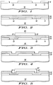
- FIG. 1 is a simplified semi-schematic drawing of a substrate 10 with a planar surface 11 and a discontinuity in the surface.
- the discontinuity is a patterned layer 12 of electrically conductive contact material, such as heavily doped gallium arsenide (GaAs), etc.
- Patterned layer 12 defines contact areas for electrodes of the semiconductor device which may be, for example, the current carrying electrodes (e.g. drain and/or source) for a FET, HFET, etc.
- the current carrying electrodes e.g. drain and/or source
- doping material may be introduced directly into substrate 10 to form the contact areas.
- Patterned layer 12 is also patterned to define control electrode area or areas 13 therebetween. In the fabrication of FETs or HFETs this area is designed to receive a gate which, as described above, is desirably as small or narrow as possible. It should be understood that substrate 10 actually represents a semiconductor wafer, only a small portion of which is illustrated. Also, while patterned layer 12 includes three different discontinuities, various combinations of current carrying electrodes in various semiconductor devices are possible and, since such details are known in the art, they will not be elaborated upon in this disclosure.
- a layer 15 of gate metal (or other electrically conductive material) is deposited on substrate 10 so as to overlie control electrode areas 13 and the discontinuities in patterned layer 12.
- a blanket layer of gate metal such as TiWN, Al, or similar metal capable of forming a good Schottky contact with the underlying material, is deposited onto the surface and substantially planarizes the structure.
- a first etchable layer 20 of material which is generally a dielectric such as Si 3 N 4 or the like, is deposited on the surface of layer 15 and patterned so as to present one or more sidewalls 21, as illustrated in FIG. 3.
- FIGS. 4 and 5 in which similar components are designated with similar numbers each having a prime added to denote a different embodiment, a slightly different embodiment is illustrated in which layer 15' is deposited conformally, so that discontinuities in layer 12' are preserved. It will of course be understood by those skilled in the art that during actual fabrication processes combinations of these two embodiments may be present and one purpose of illustrating the two possible extremes is to accentuate the fact that as long as layer 15' is thick enough to provide the desired result the surface contour is optional.
- a first etchable layer 20' is deposited on the surface of layer 15' and patterned so as to present one or more sidewalls 21', as previously described.
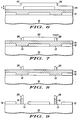
- a second etchable layer 25 is conformally deposited over layer 20 so as to define second sidewalls 26. It should be noted that second sidewalls 26 define a portion of layer 25 which is substantially thicker (approximately twice as thick) as the remainder of layer 25. Also, by correctly patterning layer 20 and sidewall 21, sidewall 26 (or the thicker portion of layer 25) is positioned at the desired location in control electrode area 13. Generally, layer 25 is formed of some easily etchable material, such as SiO 2 or the like, for reasons that will be apparent presently.
- layer 25 is etched to remove everything except sidewall 26, or the thicker portion of layer 25.
- layer 25 has a thickness 't' and by etching 't' thickness of material from layer 25 sidewalls 26 are retained.
- the width 'w' of sidewalls 26 is generally determined by the thickness 't' of layer 25.
- the width 'w' can be easily controlled by controlling the thickness 't' of layer 25, which is very accurately controllable.
- Layer 20 is now removed by any convenient method, such as a selective etch, to leave free standing sidewalls 26, as illustrated in FIG. 8.
- Layer 15 is then etched, using some convenient etch technique such as a reactive ion etch (RIE), and with sidewalls 26 acting as an etch mask, as illustrated in FIG. 9.
- RIE reactive ion etch
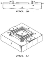
- the remaining portion or portions 30 of layer 15 define a control terminal (e.g. a gate for a FET or HFET) in control terminal area 13 for the semiconductor device.
- Portion 30 extends into and out of the paper in FIG. 10 and may be terminated to form two different portions or may be extended in the form of a rectangle, as illustrated in FIG. 11 to encircle an inner discontinuity 35.
- sidewalls 26 can be removed to leave control terminals 30, as illustrated in FIGS 10 or 11.
- portions 30 can be relatively easily fabricated in submicron sizes, for example 0.25 microns or less. Also, because the thickness of layer 25 is highly repeatable, portions 30 can be very accurately repeated over the entire wafer and over other wafers as well. Thus, semiconductor devices with submicron control electrodes are very manufacturable with very accurate and repeatable speed and frequency characteristics.
Landscapes
- Junction Field-Effect Transistors (AREA)
- Drying Of Semiconductors (AREA)
- Electrodes Of Semiconductors (AREA)
- Internal Circuitry In Semiconductor Integrated Circuit Devices (AREA)
Applications Claiming Priority (2)
| Application Number | Priority Date | Filing Date | Title |
|---|---|---|---|
| US08/566,385 US5599738A (en) | 1995-12-11 | 1995-12-11 | Methods of fabrication of submicron features in semiconductor devices |
| US566385 | 1995-12-11 |
Publications (2)
| Publication Number | Publication Date |
|---|---|
| EP0782183A2 true EP0782183A2 (de) | 1997-07-02 |
| EP0782183A3 EP0782183A3 (de) | 1997-07-16 |
Family
ID=24262673
Family Applications (1)
| Application Number | Title | Priority Date | Filing Date |
|---|---|---|---|
| EP96119205A Withdrawn EP0782183A3 (de) | 1995-12-11 | 1996-11-29 | Verfahren zur Herstellung von submikrometrischen Merkmalen in Halbleiterbauelementen |
Country Status (4)
| Country | Link |
|---|---|
| US (1) | US5599738A (de) |
| EP (1) | EP0782183A3 (de) |
| JP (1) | JPH09181337A (de) |
| KR (1) | KR970051944A (de) |
Families Citing this family (7)
| Publication number | Priority date | Publication date | Assignee | Title |
|---|---|---|---|---|
| DE19548058C2 (de) * | 1995-12-21 | 1997-11-20 | Siemens Ag | Verfahren zur Herstellung eines MOS-Transistors |
| US5851882A (en) | 1996-05-06 | 1998-12-22 | Micron Technology, Inc. | ZPROM manufacture and design and methods for forming thin structures using spacers as an etching mask |
| US5923981A (en) * | 1996-12-31 | 1999-07-13 | Intel Corporation | Cascading transistor gate and method for fabricating the same |
| US6150245A (en) * | 1997-02-27 | 2000-11-21 | Nec Corporation | Method of manufacturing a field effect transistor |
| US6191446B1 (en) | 1998-03-04 | 2001-02-20 | Advanced Micro Devices, Inc. | Formation and control of a vertically oriented transistor channel length |
| US6683337B2 (en) | 2001-02-09 | 2004-01-27 | Micron Technology, Inc. | Dynamic memory based on single electron storage |
| DE10137575A1 (de) * | 2001-07-31 | 2003-02-27 | Infineon Technologies Ag | Verfahren zur Erzeugung einer Maske sowie Verfahren zur Herstellung einer Halbleitervorrichtung |
Family Cites Families (9)
| Publication number | Priority date | Publication date | Assignee | Title |
|---|---|---|---|---|
| US4358340A (en) * | 1980-07-14 | 1982-11-09 | Texas Instruments Incorporated | Submicron patterning without using submicron lithographic technique |
| US4354896A (en) * | 1980-08-05 | 1982-10-19 | Texas Instruments Incorporated | Formation of submicron substrate element |
| US4432132A (en) * | 1981-12-07 | 1984-02-21 | Bell Telephone Laboratories, Incorporated | Formation of sidewall oxide layers by reactive oxygen ion etching to define submicron features |
| JPS60137070A (ja) * | 1983-12-26 | 1985-07-20 | Toshiba Corp | 半導体装置の製造方法 |
| US4648937A (en) * | 1985-10-30 | 1987-03-10 | International Business Machines Corporation | Method of preventing asymmetric etching of lines in sub-micrometer range sidewall images transfer |
| US4689869A (en) * | 1986-04-07 | 1987-09-01 | International Business Machines Corporation | Fabrication of insulated gate gallium arsenide FET with self-aligned source/drain and submicron channel length |
| JPS63226930A (ja) * | 1987-03-16 | 1988-09-21 | Nec Corp | 半導体装置の製造方法 |
| JPH0233939A (ja) * | 1988-07-23 | 1990-02-05 | Nec Corp | 電界効果トランジスタの製造方法 |
| US5480829A (en) * | 1993-06-25 | 1996-01-02 | Motorola, Inc. | Method of making a III-V complementary heterostructure device with compatible non-gold ohmic contacts |
-
1995
- 1995-12-11 US US08/566,385 patent/US5599738A/en not_active Expired - Fee Related
-
1996
- 1996-11-29 EP EP96119205A patent/EP0782183A3/de not_active Withdrawn
- 1996-12-04 JP JP8338959A patent/JPH09181337A/ja active Pending
- 1996-12-06 KR KR1019960062195A patent/KR970051944A/ko not_active Abandoned
Non-Patent Citations (1)
| Title |
|---|
| None |
Also Published As
| Publication number | Publication date |
|---|---|
| EP0782183A3 (de) | 1997-07-16 |
| US5599738A (en) | 1997-02-04 |
| KR970051944A (ko) | 1997-07-29 |
| JPH09181337A (ja) | 1997-07-11 |
Similar Documents
| Publication | Publication Date | Title |
|---|---|---|
| JP2778600B2 (ja) | 半導体装置の製造方法 | |
| US4711858A (en) | Method of fabricating a self-aligned metal-semiconductor FET having an insulator spacer | |
| US4546540A (en) | Self-aligned manufacture of FET | |
| US5288654A (en) | Method of making a mushroom-shaped gate electrode of semiconductor device | |
| EP0516408A2 (de) | Verfahren zur Herstellung einer T-Gatestruktur über einem Substrat mit einem mikroelektronischen Bauelement | |
| US5139968A (en) | Method of producing a t-shaped gate electrode | |
| EP0704882B1 (de) | Verfahren zur Herstellung von eng benachbarten Metallelektroden auf einer Halbleiter-Anordnung | |
| US5599738A (en) | Methods of fabrication of submicron features in semiconductor devices | |
| EP0461807B1 (de) | MESFET und Verfahren zur Herstellung | |
| US4268537A (en) | Method for manufacturing a self-aligned contact in a grooved semiconductor surface | |
| US5356823A (en) | Method of manufacturing a semiconductor device | |
| US5776805A (en) | Method for manufacturing MESFET | |
| KR0179116B1 (ko) | 자가정렬형 티형 게이트 제조방법 | |
| EP0385031B1 (de) | Halbleiteranordnung mit einem eingefügten Gate und Verfahren zur Herstellung | |
| US5719088A (en) | Method of fabricating semiconductor devices with a passivated surface | |
| JPH04250620A (ja) | 半導体素子における金属接点の自己整合方法及び自己整合性半導体 | |
| US6023087A (en) | Thin film transistor having an insulating membrane layer on a portion of its active layer | |
| KR100192973B1 (ko) | 경사진 게이트 산화막을 갖는 전력용 모스 소자및그제조방법 | |
| JP3036451B2 (ja) | 半導体装置の製造方法 | |
| KR0141780B1 (ko) | 반도체소자 제조방법 | |
| KR100309136B1 (ko) | 반도체 소자의 트랜지스터 제조방법 | |
| JP3123445B2 (ja) | 半導体装置の製造方法 | |
| KR100198425B1 (ko) | 폴리이미드를 이용한 이종접합 바이폴라 트랜지스터의 제조방법 | |
| JP3101455B2 (ja) | 電界効果トランジスタ及びその製造方法 | |
| JPH1012871A (ja) | 半導体装置の製造方法 |
Legal Events
| Date | Code | Title | Description |
|---|---|---|---|
| PUAI | Public reference made under article 153(3) epc to a published international application that has entered the european phase |
Free format text: ORIGINAL CODE: 0009012 |
|
| PUAL | Search report despatched |
Free format text: ORIGINAL CODE: 0009013 |
|
| AK | Designated contracting states |
Kind code of ref document: A2 Designated state(s): DE FR GB |
|
| AK | Designated contracting states |
Kind code of ref document: A3 Designated state(s): DE FR GB |
|
| 17P | Request for examination filed |
Effective date: 19980116 |
|
| 17Q | First examination report despatched |
Effective date: 19991005 |
|
| GRAH | Despatch of communication of intention to grant a patent |
Free format text: ORIGINAL CODE: EPIDOS IGRA |
|
| STAA | Information on the status of an ep patent application or granted ep patent |
Free format text: STATUS: THE APPLICATION IS DEEMED TO BE WITHDRAWN |
|
| 18D | Application deemed to be withdrawn |
Effective date: 20030617 |