EP0782146A2 - Nichtflüchtiger Speicher mit Datenspeicherbereich und Attributdatenbereich zum Speichern der Attributdaten des Datenspeicherbereichs - Google Patents
Nichtflüchtiger Speicher mit Datenspeicherbereich und Attributdatenbereich zum Speichern der Attributdaten des Datenspeicherbereichs Download PDFInfo
- Publication number
- EP0782146A2 EP0782146A2 EP96120955A EP96120955A EP0782146A2 EP 0782146 A2 EP0782146 A2 EP 0782146A2 EP 96120955 A EP96120955 A EP 96120955A EP 96120955 A EP96120955 A EP 96120955A EP 0782146 A2 EP0782146 A2 EP 0782146A2
- Authority
- EP
- European Patent Office
- Prior art keywords
- memory
- data
- memory cells
- sector
- block
- Prior art date
- Legal status (The legal status is an assumption and is not a legal conclusion. Google has not performed a legal analysis and makes no representation as to the accuracy of the status listed.)
- Withdrawn
Links
- 230000004044 response Effects 0.000 claims 2
- 239000004065 semiconductor Substances 0.000 description 29
- 238000010586 diagram Methods 0.000 description 25
- 238000013500 data storage Methods 0.000 description 10
- 238000004519 manufacturing process Methods 0.000 description 9
- 238000004364 calculation method Methods 0.000 description 5
- 230000000694 effects Effects 0.000 description 5
- 101000685663 Homo sapiens Sodium/nucleoside cotransporter 1 Proteins 0.000 description 3
- 102100023116 Sodium/nucleoside cotransporter 1 Human genes 0.000 description 3
- ZMRUPTIKESYGQW-UHFFFAOYSA-N propranolol hydrochloride Chemical compound [H+].[Cl-].C1=CC=C2C(OCC(O)CNC(C)C)=CC=CC2=C1 ZMRUPTIKESYGQW-UHFFFAOYSA-N 0.000 description 3
- 230000003247 decreasing effect Effects 0.000 description 2
- 101001116774 Homo sapiens Methionine-R-sulfoxide reductase B2, mitochondrial Proteins 0.000 description 1
- 102100024862 Methionine-R-sulfoxide reductase B2, mitochondrial Human genes 0.000 description 1
- 101100467813 Saccharomyces cerevisiae (strain ATCC 204508 / S288c) RBS1 gene Proteins 0.000 description 1
- 230000032683 aging Effects 0.000 description 1
- 230000010485 coping Effects 0.000 description 1
- 239000011159 matrix material Substances 0.000 description 1
- 230000002035 prolonged effect Effects 0.000 description 1
- 230000001737 promoting effect Effects 0.000 description 1
Images









Classifications
-
- G—PHYSICS
- G11—INFORMATION STORAGE
- G11C—STATIC STORES
- G11C5/00—Details of stores covered by group G11C11/00
- G11C5/02—Disposition of storage elements, e.g. in the form of a matrix array
- G11C5/025—Geometric lay-out considerations of storage- and peripheral-blocks in a semiconductor storage device
-
- G—PHYSICS
- G11—INFORMATION STORAGE
- G11C—STATIC STORES
- G11C16/00—Erasable programmable read-only memories
-
- G—PHYSICS
- G11—INFORMATION STORAGE
- G11C—STATIC STORES
- G11C16/00—Erasable programmable read-only memories
- G11C16/02—Erasable programmable read-only memories electrically programmable
- G11C16/06—Auxiliary circuits, e.g. for writing into memory
- G11C16/22—Safety or protection circuits preventing unauthorised or accidental access to memory cells
Definitions
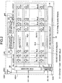
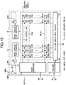
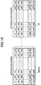
- According to the present invention includes at least one of sectors (sector is defined one word line) where sector data of a first byte number and attribute data of a second byte number corresponding to the sector data, are stored as one set of data in one row (column) or rows (columns) , are arranged, whereby an error correcting circuit in respect of data of one sector can be constituted by a circuit correcting error of one bit or bits. Therefore, a bit line failure and a memory cell failure can be relieved by the error correcting circuit whereby the manufacturing yield is promoted and the manufacturing cost can be reduced.
- a single sector can be arranged to rows of a small plural number as in the first embodiment.
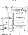
- a 1 bit error correcting circuit may be constituted to relieve the initial failure of the single word line and the circuit scale can be rendered 1 several 10s-th of that in the conventional example.
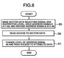
- a number of rows (a number of columns) of one sector can significantly be decreased (minimum 1 row, 1 column) and the sector data and the attribute data can continuously be accessed thereby providing an effect by which the operational speed can be accelerated.
Landscapes
- Engineering & Computer Science (AREA)
- Microelectronics & Electronic Packaging (AREA)
- Computer Security & Cryptography (AREA)
- Read Only Memory (AREA)
- Techniques For Improving Reliability Of Storages (AREA)
- For Increasing The Reliability Of Semiconductor Memories (AREA)
Applications Claiming Priority (3)
| Application Number | Priority Date | Filing Date | Title |
|---|---|---|---|
| JP34151395A JP2848300B2 (ja) | 1995-12-27 | 1995-12-27 | 不揮発性半導体記憶装置 |
| JP341513/95 | 1995-12-27 | ||
| JP34151395 | 1995-12-27 |
Publications (2)
| Publication Number | Publication Date |
|---|---|
| EP0782146A2 true EP0782146A2 (de) | 1997-07-02 |
| EP0782146A3 EP0782146A3 (de) | 2003-07-16 |
Family
ID=18346650
Family Applications (1)
| Application Number | Title | Priority Date | Filing Date |
|---|---|---|---|
| EP96120955A Withdrawn EP0782146A3 (de) | 1995-12-27 | 1996-12-27 | Nichtflüchtiger Speicher mit Datenspeicherbereich und Attributdatenbereich zum Speichern der Attributdaten des Datenspeicherbereichs |
Country Status (4)
| Country | Link |
|---|---|
| US (1) | US5818754A (de) |
| EP (1) | EP0782146A3 (de) |
| JP (1) | JP2848300B2 (de) |
| KR (1) | KR100273628B1 (de) |
Cited By (1)
| Publication number | Priority date | Publication date | Assignee | Title |
|---|---|---|---|---|
| EP1708203A1 (de) * | 2005-03-25 | 2006-10-04 | Samsung Electronics Co., Ltd. | Nichtflüchtige Speichervorrichtung und Verfahren zur Speicherung von Statusinformationen unter Verwendung mehrfacher Strings |
Families Citing this family (9)
| Publication number | Priority date | Publication date | Assignee | Title |
|---|---|---|---|---|
| EP1031992B1 (de) * | 1989-04-13 | 2006-06-21 | SanDisk Corporation | EEprom-System mit Blocklöschung |
| US7447069B1 (en) | 1989-04-13 | 2008-11-04 | Sandisk Corporation | Flash EEprom system |
| JP3411186B2 (ja) * | 1997-06-06 | 2003-05-26 | シャープ株式会社 | 不揮発性半導体記憶装置 |
| US6178532B1 (en) | 1998-06-11 | 2001-01-23 | Micron Technology, Inc. | On-chip circuit and method for testing memory devices |
| US6148414A (en) * | 1998-09-24 | 2000-11-14 | Seek Systems, Inc. | Methods and systems for implementing shared disk array management functions |
| US7266706B2 (en) * | 1999-03-03 | 2007-09-04 | Yottayotta, Inc. | Methods and systems for implementing shared disk array management functions |
| US7061792B1 (en) * | 2002-08-10 | 2006-06-13 | National Semiconductor Corporation | Low AC power SRAM architecture |
| JPWO2007023544A1 (ja) * | 2005-08-25 | 2009-03-26 | スパンション エルエルシー | 記憶装置、記憶装置の制御方法、および記憶制御装置の制御方法 |
| JP2008021390A (ja) * | 2006-07-14 | 2008-01-31 | Toshiba Corp | 半導体記憶装置 |
Citations (1)
| Publication number | Priority date | Publication date | Assignee | Title |
|---|---|---|---|---|
| JPH05189981A (ja) | 1992-01-10 | 1993-07-30 | Toshiba Corp | フラッシュ型eepromおよびそのフラッシュ型eepromを使用した電子計算機システム |
Family Cites Families (9)
| Publication number | Priority date | Publication date | Assignee | Title |
|---|---|---|---|---|
| US5268870A (en) * | 1988-06-08 | 1993-12-07 | Eliyahou Harari | Flash EEPROM system and intelligent programming and erasing methods therefor |
| JPH0748320B2 (ja) * | 1989-07-24 | 1995-05-24 | セイコー電子工業株式会社 | 半導体不揮発性メモリ |
| JPH03250499A (ja) * | 1990-02-27 | 1991-11-08 | Nec Corp | データ記憶回路 |
| JPH05151097A (ja) * | 1991-11-28 | 1993-06-18 | Fujitsu Ltd | 書換回数制限型メモリのデータ管理方式 |
| JP3251968B2 (ja) * | 1992-01-20 | 2002-01-28 | 富士通株式会社 | 半導体記憶装置 |
| ATA80592A (de) * | 1992-04-21 | 1995-06-15 | Vaillant Gmbh | Verfahren zum optimalen ausnutzen der speicherkapazität eines eeprom |
| JP2647312B2 (ja) * | 1992-09-11 | 1997-08-27 | インターナショナル・ビジネス・マシーンズ・コーポレイション | 一括消去型不揮発性半導体記憶装置 |
| US5388083A (en) * | 1993-03-26 | 1995-02-07 | Cirrus Logic, Inc. | Flash memory mass storage architecture |
| JPH08249895A (ja) * | 1995-03-10 | 1996-09-27 | Nec Corp | 不輝発性半導体記憶装置 |
-
1995
- 1995-12-27 JP JP34151395A patent/JP2848300B2/ja not_active Expired - Fee Related
-
1996
- 1996-12-27 US US08/773,900 patent/US5818754A/en not_active Expired - Lifetime
- 1996-12-27 KR KR1019960082417A patent/KR100273628B1/ko not_active Expired - Fee Related
- 1996-12-27 EP EP96120955A patent/EP0782146A3/de not_active Withdrawn
Patent Citations (1)
| Publication number | Priority date | Publication date | Assignee | Title |
|---|---|---|---|---|
| JPH05189981A (ja) | 1992-01-10 | 1993-07-30 | Toshiba Corp | フラッシュ型eepromおよびそのフラッシュ型eepromを使用した電子計算機システム |
Cited By (2)
| Publication number | Priority date | Publication date | Assignee | Title |
|---|---|---|---|---|
| EP1708203A1 (de) * | 2005-03-25 | 2006-10-04 | Samsung Electronics Co., Ltd. | Nichtflüchtige Speichervorrichtung und Verfahren zur Speicherung von Statusinformationen unter Verwendung mehrfacher Strings |
| US7457911B2 (en) | 2005-03-25 | 2008-11-25 | Samsung Electronics Co., Ltd. | Nonvolatile memory device and method for storing status information using multiple strings |
Also Published As
| Publication number | Publication date |
|---|---|
| JP2848300B2 (ja) | 1999-01-20 |
| KR100273628B1 (ko) | 2001-01-15 |
| US5818754A (en) | 1998-10-06 |
| KR970051327A (ko) | 1997-07-29 |
| EP0782146A3 (de) | 2003-07-16 |
| JPH09180485A (ja) | 1997-07-11 |
Similar Documents
| Publication | Publication Date | Title |
|---|---|---|
| US7403436B2 (en) | Non-volatile semiconductor memory device | |
| US5313425A (en) | Semiconductor memory device having an improved error correction capability | |
| US6314032B2 (en) | Semiconductor device with flexible redundancy system | |
| US7219271B2 (en) | Memory device and method for redundancy/self-repair | |
| US5524231A (en) | Nonvolatile memory card with an address table and an address translation logic for mapping out defective blocks within the memory card | |
| EP0660237B1 (de) | Halbleiterspeichergerät mit einem Ersatzspeicherzellfeld | |
| US7149135B2 (en) | Multi chip package type memory system and a replacement method of replacing a defect therein | |
| US5033024A (en) | Matrix memory with redundancy and minimizes delay | |
| US5818754A (en) | Nonvolatile memory having data storing area and attribute data area for storing attribute data of data storing area | |
| US6457093B2 (en) | Circuit and method to control operations of another circuit | |
| US8064258B2 (en) | Method apparatus, and system providing adjustable memory page configuration | |
| EP0153752B1 (de) | Halbleiterspeichergerät mit einer Bit-Fehlererkennungsfunktion | |
| JPH07141478A (ja) | 受動ユニット計数集積回路 | |
| KR100305033B1 (ko) | 블럭 아키텍츄어 옵션 회로를 구비하는 불휘발성 반도체 메모리 장치 | |
| US6728136B2 (en) | Electronically rewritable non-volatile semiconductor memory device | |
| EP0428396A2 (de) | Bitfehlerkorrekturschaltung für einen nichtflüchtigen Speicher | |
| JP3482543B2 (ja) | 半導体メモリ | |
| US6091641A (en) | Non-volatile memory device and method for the programming of the same | |
| US5226015A (en) | Semiconductor memory system | |
| KR100449269B1 (ko) | 고집적을 위한 불휘발성 반도체 메모리 장치 | |
| JPH0528779A (ja) | 不揮発性メモリ装置 | |
| JP3970391B2 (ja) | 不揮発性半導体記憶装置 | |
| JPH065082A (ja) | 半導体記憶装置 |
Legal Events
| Date | Code | Title | Description |
|---|---|---|---|
| PUAI | Public reference made under article 153(3) epc to a published international application that has entered the european phase |
Free format text: ORIGINAL CODE: 0009012 |
|
| AK | Designated contracting states |
Kind code of ref document: A2 Designated state(s): DE FR GB |
|
| RAP1 | Party data changed (applicant data changed or rights of an application transferred) |
Owner name: NEC ELECTRONICS CORPORATION |
|
| PUAL | Search report despatched |
Free format text: ORIGINAL CODE: 0009013 |
|
| AK | Designated contracting states |
Designated state(s): DE FR GB |
|
| RIC1 | Information provided on ipc code assigned before grant |
Ipc: 7G 11C 16/34 B Ipc: 7G 11C 16/06 B Ipc: 7G 11C 16/04 A |
|
| 17P | Request for examination filed |
Effective date: 20031120 |
|
| GRAP | Despatch of communication of intention to grant a patent |
Free format text: ORIGINAL CODE: EPIDOSNIGR1 |
|
| STAA | Information on the status of an ep patent application or granted ep patent |
Free format text: STATUS: THE APPLICATION IS DEEMED TO BE WITHDRAWN |
|
| 18D | Application deemed to be withdrawn |
Effective date: 20041210 |