EP0780913B1 - Elément piézo-électrique à couche mince et tête d'écriture à jet d'encre produite à l'aide dudit élément - Google Patents
Elément piézo-électrique à couche mince et tête d'écriture à jet d'encre produite à l'aide dudit élément Download PDFInfo
- Publication number
- EP0780913B1 EP0780913B1 EP96120623A EP96120623A EP0780913B1 EP 0780913 B1 EP0780913 B1 EP 0780913B1 EP 96120623 A EP96120623 A EP 96120623A EP 96120623 A EP96120623 A EP 96120623A EP 0780913 B1 EP0780913 B1 EP 0780913B1
- Authority
- EP
- European Patent Office
- Prior art keywords
- film
- ink
- piezoelectric
- lower electrode
- jet recording
- Prior art date
- Legal status (The legal status is an assumption and is not a legal conclusion. Google has not performed a legal analysis and makes no representation as to the accuracy of the status listed.)
- Expired - Lifetime
Links
- 239000010409 thin film Substances 0.000 title claims description 40
- 239000010408 film Substances 0.000 claims description 195
- BASFCYQUMIYNBI-UHFFFAOYSA-N platinum Chemical compound [Pt] BASFCYQUMIYNBI-UHFFFAOYSA-N 0.000 claims description 152
- VYPSYNLAJGMNEJ-UHFFFAOYSA-N Silicium dioxide Chemical compound O=[Si]=O VYPSYNLAJGMNEJ-UHFFFAOYSA-N 0.000 claims description 106
- 229910052697 platinum Inorganic materials 0.000 claims description 76
- 239000000377 silicon dioxide Substances 0.000 claims description 53
- 235000012239 silicon dioxide Nutrition 0.000 claims description 53
- 229910052451 lead zirconate titanate Inorganic materials 0.000 claims description 22
- 239000000758 substrate Substances 0.000 claims description 18
- GWEVSGVZZGPLCZ-UHFFFAOYSA-N Titan oxide Chemical compound O=[Ti]=O GWEVSGVZZGPLCZ-UHFFFAOYSA-N 0.000 claims description 15
- OGIDPMRJRNCKJF-UHFFFAOYSA-N titanium oxide Inorganic materials [Ti]=O OGIDPMRJRNCKJF-UHFFFAOYSA-N 0.000 claims description 11
- 238000003980 solgel method Methods 0.000 claims description 7
- HFGPZNIAWCZYJU-UHFFFAOYSA-N lead zirconate titanate Chemical compound [O-2].[O-2].[O-2].[O-2].[O-2].[Ti+4].[Zr+4].[Pb+2] HFGPZNIAWCZYJU-UHFFFAOYSA-N 0.000 claims description 5
- 229910019653 Mg1/3Nb2/3 Inorganic materials 0.000 claims description 4
- 238000007789 sealing Methods 0.000 claims description 4
- 230000010355 oscillation Effects 0.000 claims description 2
- 239000010410 layer Substances 0.000 description 37
- XUIMIQQOPSSXEZ-UHFFFAOYSA-N Silicon Chemical compound [Si] XUIMIQQOPSSXEZ-UHFFFAOYSA-N 0.000 description 15
- 238000000926 separation method Methods 0.000 description 15
- 229910052710 silicon Inorganic materials 0.000 description 15
- 239000010703 silicon Substances 0.000 description 15
- 239000010936 titanium Substances 0.000 description 11
- RTAQQCXQSZGOHL-UHFFFAOYSA-N Titanium Chemical compound [Ti] RTAQQCXQSZGOHL-UHFFFAOYSA-N 0.000 description 10
- 229910052719 titanium Inorganic materials 0.000 description 10
- 238000005530 etching Methods 0.000 description 7
- 238000000034 method Methods 0.000 description 7
- KWYUFKZDYYNOTN-UHFFFAOYSA-M Potassium hydroxide Chemical compound [OH-].[K+] KWYUFKZDYYNOTN-UHFFFAOYSA-M 0.000 description 6
- 238000004519 manufacturing process Methods 0.000 description 5
- QVGXLLKOCUKJST-UHFFFAOYSA-N atomic oxygen Chemical compound [O] QVGXLLKOCUKJST-UHFFFAOYSA-N 0.000 description 4
- 238000007641 inkjet printing Methods 0.000 description 4
- 229910052760 oxygen Inorganic materials 0.000 description 4
- 239000001301 oxygen Substances 0.000 description 4
- 238000004544 sputter deposition Methods 0.000 description 4
- XLYOFNOQVPJJNP-UHFFFAOYSA-N water Substances O XLYOFNOQVPJJNP-UHFFFAOYSA-N 0.000 description 4
- QTBSBXVTEAMEQO-UHFFFAOYSA-N Acetic acid Chemical compound CC(O)=O QTBSBXVTEAMEQO-UHFFFAOYSA-N 0.000 description 3
- KRHYYFGTRYWZRS-UHFFFAOYSA-N Fluorane Chemical compound F KRHYYFGTRYWZRS-UHFFFAOYSA-N 0.000 description 3
- 230000002950 deficient Effects 0.000 description 3
- 238000011156 evaluation Methods 0.000 description 3
- 238000010438 heat treatment Methods 0.000 description 3
- 229960002050 hydrofluoric acid Drugs 0.000 description 3
- 238000004151 rapid thermal annealing Methods 0.000 description 3
- 238000005245 sintering Methods 0.000 description 3
- DDFHBQSCUXNBSA-UHFFFAOYSA-N 5-(5-carboxythiophen-2-yl)thiophene-2-carboxylic acid Chemical compound S1C(C(=O)O)=CC=C1C1=CC=C(C(O)=O)S1 DDFHBQSCUXNBSA-UHFFFAOYSA-N 0.000 description 2
- PXHVJJICTQNCMI-UHFFFAOYSA-N Nickel Chemical compound [Ni] PXHVJJICTQNCMI-UHFFFAOYSA-N 0.000 description 2
- YRKCREAYFQTBPV-UHFFFAOYSA-N acetylacetone Chemical compound CC(=O)CC(C)=O YRKCREAYFQTBPV-UHFFFAOYSA-N 0.000 description 2
- 230000000052 comparative effect Effects 0.000 description 2
- 230000000694 effects Effects 0.000 description 2
- 230000001939 inductive effect Effects 0.000 description 2
- 238000007254 oxidation reaction Methods 0.000 description 2
- 229920002120 photoresistant polymer Polymers 0.000 description 2
- 235000011118 potassium hydroxide Nutrition 0.000 description 2
- 238000005546 reactive sputtering Methods 0.000 description 2
- 239000004408 titanium dioxide Substances 0.000 description 2
- VXUYXOFXAQZZMF-UHFFFAOYSA-N titanium(IV) isopropoxide Chemical compound CC(C)O[Ti](OC(C)C)(OC(C)C)OC(C)C VXUYXOFXAQZZMF-UHFFFAOYSA-N 0.000 description 2
- ZNQVEEAIQZEUHB-UHFFFAOYSA-N 2-ethoxyethanol Chemical compound CCOCCO ZNQVEEAIQZEUHB-UHFFFAOYSA-N 0.000 description 1
- VYZAMTAEIAYCRO-UHFFFAOYSA-N Chromium Chemical compound [Cr] VYZAMTAEIAYCRO-UHFFFAOYSA-N 0.000 description 1
- NMUTVZGCFBKTRR-UHFFFAOYSA-N acetyl acetate;zirconium Chemical compound [Zr].CC(=O)OC(C)=O NMUTVZGCFBKTRR-UHFFFAOYSA-N 0.000 description 1
- XAGFODPZIPBFFR-UHFFFAOYSA-N aluminium Chemical compound [Al] XAGFODPZIPBFFR-UHFFFAOYSA-N 0.000 description 1
- 229910052782 aluminium Inorganic materials 0.000 description 1
- 238000000137 annealing Methods 0.000 description 1
- 230000015572 biosynthetic process Effects 0.000 description 1
- 238000005229 chemical vapour deposition Methods 0.000 description 1
- 239000011248 coating agent Substances 0.000 description 1
- 238000000576 coating method Methods 0.000 description 1
- 238000007796 conventional method Methods 0.000 description 1
- 230000008878 coupling Effects 0.000 description 1
- 238000010168 coupling process Methods 0.000 description 1
- 238000005859 coupling reaction Methods 0.000 description 1
- 238000006073 displacement reaction Methods 0.000 description 1
- 238000000608 laser ablation Methods 0.000 description 1
- 229940046892 lead acetate Drugs 0.000 description 1
- 239000011777 magnesium Substances 0.000 description 1
- UEGPKNKPLBYCNK-UHFFFAOYSA-L magnesium acetate Chemical compound [Mg+2].CC([O-])=O.CC([O-])=O UEGPKNKPLBYCNK-UHFFFAOYSA-L 0.000 description 1
- 235000011285 magnesium acetate Nutrition 0.000 description 1
- 239000011654 magnesium acetate Substances 0.000 description 1
- 229940069446 magnesium acetate Drugs 0.000 description 1
- 239000000463 material Substances 0.000 description 1
- 229910044991 metal oxide Inorganic materials 0.000 description 1
- 229910052759 nickel Inorganic materials 0.000 description 1
- 230000003647 oxidation Effects 0.000 description 1
- 230000010287 polarization Effects 0.000 description 1
- 229920001451 polypropylene glycol Polymers 0.000 description 1
- 239000002356 single layer Substances 0.000 description 1
- 239000007787 solid Substances 0.000 description 1
- 238000004528 spin coating Methods 0.000 description 1
- 238000000992 sputter etching Methods 0.000 description 1
Images

Classifications
-
- B—PERFORMING OPERATIONS; TRANSPORTING
- B41—PRINTING; LINING MACHINES; TYPEWRITERS; STAMPS
- B41J—TYPEWRITERS; SELECTIVE PRINTING MECHANISMS, i.e. MECHANISMS PRINTING OTHERWISE THAN FROM A FORME; CORRECTION OF TYPOGRAPHICAL ERRORS
- B41J2/00—Typewriters or selective printing mechanisms characterised by the printing or marking process for which they are designed
- B41J2/005—Typewriters or selective printing mechanisms characterised by the printing or marking process for which they are designed characterised by bringing liquid or particles selectively into contact with a printing material
- B41J2/01—Ink jet
- B41J2/135—Nozzles
- B41J2/16—Production of nozzles
- B41J2/1621—Manufacturing processes
- B41J2/164—Manufacturing processes thin film formation
- B41J2/1646—Manufacturing processes thin film formation thin film formation by sputtering
-
- B—PERFORMING OPERATIONS; TRANSPORTING
- B41—PRINTING; LINING MACHINES; TYPEWRITERS; STAMPS
- B41J—TYPEWRITERS; SELECTIVE PRINTING MECHANISMS, i.e. MECHANISMS PRINTING OTHERWISE THAN FROM A FORME; CORRECTION OF TYPOGRAPHICAL ERRORS
- B41J2/00—Typewriters or selective printing mechanisms characterised by the printing or marking process for which they are designed
- B41J2/005—Typewriters or selective printing mechanisms characterised by the printing or marking process for which they are designed characterised by bringing liquid or particles selectively into contact with a printing material
- B41J2/01—Ink jet
- B41J2/135—Nozzles
- B41J2/16—Production of nozzles
- B41J2/1607—Production of print heads with piezoelectric elements
- B41J2/161—Production of print heads with piezoelectric elements of film type, deformed by bending and disposed on a diaphragm
-
- B—PERFORMING OPERATIONS; TRANSPORTING
- B41—PRINTING; LINING MACHINES; TYPEWRITERS; STAMPS
- B41J—TYPEWRITERS; SELECTIVE PRINTING MECHANISMS, i.e. MECHANISMS PRINTING OTHERWISE THAN FROM A FORME; CORRECTION OF TYPOGRAPHICAL ERRORS
- B41J2/00—Typewriters or selective printing mechanisms characterised by the printing or marking process for which they are designed
- B41J2/005—Typewriters or selective printing mechanisms characterised by the printing or marking process for which they are designed characterised by bringing liquid or particles selectively into contact with a printing material
- B41J2/01—Ink jet
- B41J2/135—Nozzles
- B41J2/16—Production of nozzles
- B41J2/1621—Manufacturing processes
- B41J2/1626—Manufacturing processes etching
- B41J2/1629—Manufacturing processes etching wet etching
-
- B—PERFORMING OPERATIONS; TRANSPORTING
- B41—PRINTING; LINING MACHINES; TYPEWRITERS; STAMPS
- B41J—TYPEWRITERS; SELECTIVE PRINTING MECHANISMS, i.e. MECHANISMS PRINTING OTHERWISE THAN FROM A FORME; CORRECTION OF TYPOGRAPHICAL ERRORS
- B41J2/00—Typewriters or selective printing mechanisms characterised by the printing or marking process for which they are designed
- B41J2/005—Typewriters or selective printing mechanisms characterised by the printing or marking process for which they are designed characterised by bringing liquid or particles selectively into contact with a printing material
- B41J2/01—Ink jet
- B41J2/135—Nozzles
- B41J2/16—Production of nozzles
- B41J2/1621—Manufacturing processes
- B41J2/1631—Manufacturing processes photolithography
-
- B—PERFORMING OPERATIONS; TRANSPORTING
- B41—PRINTING; LINING MACHINES; TYPEWRITERS; STAMPS
- B41J—TYPEWRITERS; SELECTIVE PRINTING MECHANISMS, i.e. MECHANISMS PRINTING OTHERWISE THAN FROM A FORME; CORRECTION OF TYPOGRAPHICAL ERRORS
- B41J2/00—Typewriters or selective printing mechanisms characterised by the printing or marking process for which they are designed
- B41J2/005—Typewriters or selective printing mechanisms characterised by the printing or marking process for which they are designed characterised by bringing liquid or particles selectively into contact with a printing material
- B41J2/01—Ink jet
- B41J2/135—Nozzles
- B41J2/16—Production of nozzles
- B41J2/1621—Manufacturing processes
- B41J2/164—Manufacturing processes thin film formation
- B41J2/1645—Manufacturing processes thin film formation thin film formation by spincoating
-
- H—ELECTRICITY
- H10—SEMICONDUCTOR DEVICES; ELECTRIC SOLID-STATE DEVICES NOT OTHERWISE PROVIDED FOR
- H10N—ELECTRIC SOLID-STATE DEVICES NOT OTHERWISE PROVIDED FOR
- H10N30/00—Piezoelectric or electrostrictive devices
- H10N30/20—Piezoelectric or electrostrictive devices with electrical input and mechanical output, e.g. functioning as actuators or vibrators
- H10N30/204—Piezoelectric or electrostrictive devices with electrical input and mechanical output, e.g. functioning as actuators or vibrators using bending displacement, e.g. unimorph, bimorph or multimorph cantilever or membrane benders
- H10N30/2047—Membrane type
Definitions
- the present invention relates to a piezoelectric thin-film element and an ink-jet recording head using the same.
- an oscillator acting as a driving source for jetting ink is constituted by a piezoelectric thin-film element.
- this piezoelectric thin-film element has a structure provided with a piezoelectric thin film comprising polycrystal, and upper and lower electrodes disposed so as to hold this piezoelectric thin film therebetween.
- This piezoelectric thin film is generally composed of a two-component system mainly containing lead zirconate titanate (hereinafter abbreviated to "PZT"), or a three-component system in which a third component is added to the PZT of this two-component system.
- the piezoelectric thin film having such a composition can be formed, for example, by a sputtering method, a sol-gel method, a laser ablation method, a CVD method or the like.
- a silicon dioxide film is formed to be 2,500 ⁇ on a monocrystal silicon substrate by a thermal oxidation method
- a lower electrode layer of aluminum, nickel, chrome, platinum or the like is laminated thereon with a thickness of about 0.2 ⁇ m.
- a PZT film as a piezoelectric element is laminated on the lower electrode layer with a thickness of 2 to 10 ⁇ m by a sol-gel method.
- a desired process such as etching, or the like, is effected selectively from the back surface of the monocrystal silicon substrate to thereby form an ink chamber. In such a manner, an ink-jet recording head is formed.
- Such an ink-jet recording head is disposed in a printer or the like. Today, however, higher resolution is requested to be realized.
- the thickness of the piezoelectric film is made to be 5 ⁇ m or less, the boundary adhesion between the silicon dioxide film and the lower electrode film or between the lower electrode film and the PZT film is so reduced that there arises a problem that the reliability is deteriorated by the separation of the PZT film, the floating of the PZT film caused by the stress of the silicon dioxide film, and so on.
- the composition of the piezoelectric film not two-component PZT but three-component PZT.
- the composition of the piezoelectric film is made to be three-component PZT, it is necessary to make PZT be subjected to heat treatment at burning temperature of 800 °C, so that there is a problem that the adhesion between the lower electrode film and the PZT film is reduced.
- the present invention provides a piezoelectric thin-film element having a silicon dioxide film formed on a substrate, a platinum lower electrode formed on the silicon dioxide film, a piezoelectric film formed on the platinum lower electrode, and an upper electrode formed on the piezoelectric film; wherein the relationship between the film thickness (X) of the platinum lower electrode and the film thickness (Y) of the silicon dioxide film satisfies conditions of 0.5 ⁇ X/Y ⁇ 4 , and 3,000 ⁇ ⁇ X ⁇ 2 ⁇ m.
- An intermediate layer may be interposed between the silicon dioxide film and the platinum lower electrode.
- the adhesion of the platinum lower electrode or the piezoelectric film is improved, so that high durability can be obtained and the reliability can be improved.
- the adhesion of the platinum lower electrode is apt to be deteriorated by heat treatment at about 900 °C applied when the PZT film is sintered.
- the thickness (X) of the platinum lower electrode exceeds 2 ⁇ m (X>2 ⁇ m)
- the shrinkage of the platinum lower electrode becomes large by the heat applied when the PZT film is sintered, so that the adhesion of the platinum lower electrode is apt to deteriorate.
- the relationship between the film thickness (X) of the platinum lower electrode and the film thickness (Y) of the silicon dioxide film may be made to satisfy conditions of 1 ⁇ X/Y ⁇ 3, and 3,000 ⁇ ⁇ X ⁇ 1.5 ⁇ m. With such a relationship, the above advantage is more improved.
- the intermediate layer may contain at least titanium oxide.
- the adhesion of the platinum lower electrode film can be further improved.
- the thickness of the intermediate layer may be set to be in a range of from 200 ⁇ to 1,500 ⁇ .
- the piezoelectric film may comprising lead zirconate titanate.
- the piezoelectric distortion constant of this piezoelectric thin-film element can be made large. It is therefore possible to jet ink with high density when such a piezoelectric thin-film element is applied to an ink-jet recording head.
- the piezoelectric film may be formed by a sol-gel method.
- the present invention provides an ink-jet recording head comprising: a base having an ink chamber formed therein; a diaphragm sealing one side of the ink chamber and having a surface to which a piezoelectric thin-film element of a deflection oscillation mode is fixed; and a nozzle plate sealing the other side of the ink chamber and having a nozzle aperture formed therein for jetting ink; wherein the piezoelectric thin-film element is constituted by a piezoelectric thin-film element described above.
- the ink-jet recording head having such a structure not only high resolution can be attained but also high reliability can be obtained.
- the piezoelectric film may be formed only in an area corresponding to the ink chamber. With this formation, the above-mentioned advantage can be more improved.
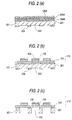
- Fig. 1(a) is a perspective view illustrating an outline of an ink-jet recording head in an embodiment of the present invention
- Fig. 1(b) is an expanded sectional view taken on line A-A' in Fig. 1(a)
- Figs. 2(a) to 2(c) are sectional views illustrating processes to manufacture the ink-jet recording head shown in Fig. 1(a).
- the ink-jet recording head according to Embodiment 1 is designed so as to have a monocrystal silicon substrate 101 in which a plurality of ink chambers 102 are formed, a piezoelectric thin-film element 110 formed on the monocrystal silicon substrate 101 through a silicon dioxide film 201, and a nozzle plate 107 which seals the ink chambers on the side opposite to the above-mentioned piezoelectric thin-film element 110 and which has nozzle apertures 108 formed therein for jetting ink.
- the piezoelectric thin-film element 110 is constituted by a platinum lower electrode 104, a piezoelectric film 105 and an upper electrode 106 formed sequentially in this order from the monocrystal silicon substrate 101 side.
- the piezoelectric film 105 and the upper electrode 106 are disposed in positions corresponding to the ink chambers 102, respectively.
- the ink chambers 102 and the nozzle apertures 108 are disposed with the same pitch as shown particularly in Fig. 1(b).
- the silicon dioxide film 201 is not formed in positions corresponding to the ink chambers 102.
- the length of the ink chamber 102 in the direction of array of the ink chambers 102 was set to 100 ⁇ m, and the length of the ink chamber 102 in the depthwise direction thereof was set to 4 mm. Further, the pitch in the direction of array of the ink chambers 102 was set to 141 ⁇ m, and the resolution was set to 180 dpi (dot per inch). In addition, the length of the piezoelectric film 105 in the direction of array was set to 80 ⁇ m.
- the ink-jet recording head according to Embodiment 1 has such a structure that the piezoelectric film 105 is formed only in an area corresponding to the ink chambers 102, and the piezoelectric film 105 is not formed in the area where the ink chambers 102 are not formed in the direction of array thereof.
- the ink-jet recording head having such a structure when a voltage is applied to transform the ink chambers 102, a large displacement can be obtained even if the applied voltage is small in comparison with an ink-jet recording head in which a piezoelectric film is formed also in the area where ink chambers are not formed.
- the monocrystal silicon substrate 101 (substrate thickness: 220 ⁇ m) having surface orientation (110) is subjected to wet thermal oxidization at the temperature of about 1,200 °C so as to form silicon dioxide films 201 and 202 on the opposite sides of the monocrystal silicon substrate 101 at the same time.
- a platinum lower electrode forming film 104A, a piezoelectric film forming film 105A and an upper electrode forming film 106A are formed sequentially on this silicon dioxide film 201.
- a titanium film (film thickness: 250 ⁇ ), a titanium dioxide film (film thickness: 200 ⁇ ) and a titanium film (film thickness: 50 ⁇ ) were formed sequentially between the silicon dioxide film 201 and the platinum lower electrode forming film 104A as intermediate films for improving the adhesion of the films 201 and 104A.
- These four intermediate layers and the platinum lower electrode forming film 104A were formed continuously by a DC sputtering method.
- the titanium dioxide film was formed by a reactive sputtering method with 10% oxygen atmosphere.
- the piezoelectric film forming film 105A was formed to be 3 ⁇ m thick by a sol-gel method. At that time, 0.105 mol of lead acetate, 0.045 mol of zirconium acetyl acetate, 0.005 mol of magnesium acetate and 30 ml of acetic acid were heated to 100 °C to as to be dissolved, and thereafter cooled to the room temperature; 0.040 mol of titanium tetraisopropoxide and 0.010 mol of pentaethoxyniobate were dissolved into 50 ml of ethyl cellosolve and added thereto; 30 ml of acetylacetone was added thereto so as to stabilize; and thereafter polypropylene glycol (average molecular weight 400) was added by 30 weight % to the metallic oxide in the sol, and agitated well so that the uniform sol was obtained as material for the piezoelectric film forming film 105A to be formed by the sol-gel method.
- the thus prepared sol was applied onto the platinum lower electrode forming film 104A by spin coating and temporarily sintered at 400 °C so as to form an amorphous porous gel thin film 0.3 ⁇ m thick. Further, the steps of coating with the sol and temporary sintering at 400 °C were repeated twice so as to form a porous gel thin film 0.9 ⁇ m thick. Next, the thin film was heated to 650 °C for 5 seconds in oxygen atmosphere by RTA (Rapid Thermal Annealing), and kept in this state for 1 minute to perform preannealing to thereby form a minute thin film 0.6 ⁇ m thick. These steps were repeated five times so as to obtain an amorphous minute thin film 3.0 ⁇ m thick.
- RTA Rapid Thermal Annealing
- the thin film was heated to 900 °C in oxygen atmosphere by RTA, and kept in this state for 1 minute to perform annealing.
- the piezoelectric film forming film 105A 3.0 ⁇ m thick was obtained in such a manner.
- the obtained piezoelectric film forming film 105A was dissolved by fluoric acid, and quantatively determined by ICP (plasma emission analysis), the molar ratio (Pb:Mg:Nb:Zr:Ti) was (1.00:0.05:0.10:0.45:0.40).
- the upper electrode forming film 106A comprising platinum is formed to be 200 ⁇ thick on the obtained piezoelectric film forming film 105A by a DC sputtering method.
- a photo resist film (not-shown) is formed on the silicon dioxide film 202, and the portions of this photo resist film corresponding to the areas where the ink chambers 102 will be formed are removed selectively so as to form a photo mask (not-shown).
- the silicon dioxide film 202 is patterned with a water solution of fluoric acid and ammonium fluoride so as to form aperture portions 203.
- the depthwise direction of these aperture portions 203 that is, the direction perpendicular to the paper of drawing is defined as the ⁇ 112> direction of the monocrystal silicon substrate 101.
- a photo mask (not-shown) is formed on the upper electrode forming film 106 in the portion corresponding to the area where the upper electrode will be formed.
- the upper electrode forming film 106A and the piezoelectric film forming film 105A are etched by ion milling so as to form the upper electrode 106 and the piezoelectric film 105.
- the lower platinum electrode forming film 104A is patterned to obtain the platinum lower electrode 104.
- the piezoelectric thin-film element 110 constituted by the upper electrode 106, the piezoelectric film 105 and the platinum lower electrode 104 was formed in such a manner.
- the monocrystal silicon substrate 101 is protected by a jig (not-shown) at the side where the piezoelectric thin-film element 110 is formed.
- this substrate is immersed in a water solution of potassium hydrate which is heated to 80 °C, and anisotropic etching is performed on the monocrystal silicon film 101 by using, as a mask, the silicon dioxide film 202 having the aperture portions 203 formed therein until the silicon dioxide film 201 is exposed.
- the surfaces of the depthwise side walls of the ink chambers 102 can be made (111) surfaces.
- the ratio of etching rate between the (110) surface and the (111) surface of the monocrystal silicon substrate 101 becomes about 300:1, so that grooves 220 ⁇ m deep in the monocrystal silicon substrate 101 can be limited to about 1 ⁇ m side etching. Accordingly, the ink chambers 102 can be formed accurately.
- the silicon dioxide film 202 and the exposed silicon dioxide film 201 are etched so as to be removed with a water solution of fluoric acid and ammonium fluoride.
- the ink chambers 102 were formed in such a manner.
- the unit of film thickness was expressed by ⁇ m.
- the frequencies of occurrence were evaluated per head.
- the number of nozzles of an ink-jet recording head in this embodiment was 128, and it was determined that failure occurred even when floating or separation of a film appeared in only one of the nozzles. Criteria were set as follow.
- the film thickness of the platinum lower electrode exceeds 2 ⁇ m, the shrinkage of the platinum lower electrode is made large by heat applied when the piezoelectric film is sintered, so that the adhesion of the platinum lower electrode is apt to decrease.
- the film thicknesses of the silicon dioxide film and the platinum lower electrode it is preferable to set the film thicknesses of the silicon dioxide film and the platinum lower electrode to satisfy the condition that 1 ⁇ (the thickness of the platinum lower electrode) / (the thickness of the silicon dioxide film) ⁇ 3 and to set the film thickness of the platinum lower electrode to satisfy the condition that 3,000 ⁇ ⁇ (the thickness of the platinum lower electrode) ⁇ 1.5 ⁇ m.
- an ink-jet recording head having the same structure as the sample number 14 shown in Table 1 was prepared, and its durability was examined.
- This examination employed such a method that a rectangular waveform voltage with a pulse width if 1 millisecond and a voltage of 30 V was applied to a piezoelectric thin-film element 1 ⁇ 10 8 times, and ink jetting was evaluated before and after the application of the voltage. As a result, it could be confirmed that there was no change in the ink-jet recording head having such a structure, so that its reliability was extremely high.
- the present invention is not limited to this, but the silicon dioxide film 201 exposed in the ink chambers 102 may be partly removed, or the whole of the silicon dioxide film 201 may be left as it is without being removed. Even in this case, it is a matter of course that similar effects can be obtained because the monocrystal silicon film having supported the compressive stress of the silicon dioxide film is removed in the same manner as in Embodiment 1 when the ink chambers 102 are formed.
- the piezoelectric distortion constant is low to be about 100 pC/N in a piezoelectric film of a two-component system so that the thickness necessary for sufficient ink jetting is larger than that a
- the thickness of the piezoelectric film is set to 3 ⁇ m in Embodiment 1, the present invention is not limited to this. Effects similar to those mentioned above can be obtained if the thickness of the piezoelectric film is set to 5 ⁇ m or less, because the separation of the piezoelectric film is caused by breaking in the balance of stress between the silicon dioxide film and the platinum lower electrode.
- the intermediate layer was made to be a single-layer or multi-layer film, and a first titanium layer, a titanium oxide layer and a second titanium layer were formed sequentially on the silicon dioxide film 201.
- the four layers, including the first titanium layer, the titanium oxide layer and the second titanium layer, constituting the intermediate layer, and the platinum lower electrode 104 were formed continuously by a DC sputtering method.
- the titanium oxide layer was formed by a reactive sputtering method with 10% oxygen atmosphere.
- the structure and manufacturing process of the other films were the same as in Embodiment 1.
- the structure of the intermediate layer and the evaluation result are shown in Table 2.
- the unit of film thickness was expressed by ⁇ , and the unit of piezoelectric distortion constant was expressed by pC/N. Criteria were set as follow.
- the adhesion of the platinum lower electrode is extremely low when the intermediate layer does not include a titanium oxide layer. It was further proved that the intermediate layer does not have a function as an adhesion layer with respect to the platinum lower electrode when the intermediate layer is thinner than 200 ⁇ even if the intermediate layer includes a titanium oxide layer. Further, if the film thickness of the intermediate layer exceeds 500 ⁇ , it is possible to ensure the adhesion, but the piezoelectric distortion constant becomes small so that it is not suitable for making the density high.
- the film thickness of the first titanium layer formed on the silicon dioxide film 201 side it is particularly preferable to set the film thickness of the first titanium layer formed on the silicon dioxide film 201 side to be in a range of from 200 to 400 ⁇ , to set the film thickness of the titanium oxide layer to be in a range of from 100 to 300 ⁇ , and to set the film thickness of the second titanium layer formed on the titanium oxide layer to be in a range of 50 to 100 ⁇ .
- the intermediate layer is designed so as to have such a configuration, and if the film thickness of the intermediate layer is set to be in a range of from 200 to 1,500 ⁇ , more preferably in a range of from 300 to 800 ⁇ , it is possible to obtain a piezoelectric element superior in the adhesion of the platinum lower electrode and superior in the piezoelectric properties.
- the present invention it is possible to prevent a platinum lower electrode from separating or prevent a piezoelectric film from floating/separating, even in high-temperature treatment of a piezoelectric film of a three-component system which is indispensable for obtaining a large piezoelectric distortion constant. It is therefore possible to obtain a piezoelectric element superior in durability and high in reliability. Further, by using this piezoelectric thin-film element, it is possible to obtain an ink-jet recording head in which high resolution and high reliability can be attained. In addition, since the piezoelectric element can be made to be a thin film, it is possible to obtain an ink-jet recording head with high resolution.
Claims (17)
- Elément piézoélectrique à couches minces, comprenant :un substrat (101),une couche (201) de bioxyde de silicium formée sur le substrat,une électrode inférieure de platine (104) formée sur la couche de bioxyde de silicium,une couche piézoélectrique (105) formée sur l'électrode inférieure de platine, etune électrode supérieure (106) formée sur la couche piézoélectrique, caractérisé en ce que la relation entre l'épaisseur (X) de la couche d'électrode inférieure de platine et l'épaisseur (Y) de la couche de bioxyde de silicium correspond aux conditions suivantes :
- Elément piézoélectrique à couches minces selon la revendication 1, dans lequel une couche intermédiaire est formée entre la couche (201) de bioxyde de silicium et l'électrode inférieure (104) de platine.
- Elément piézoélectrique à couches minces selon la revendication 1, dans lequel la relation entre l'épaisseur (X) de la couche d'électrode inférieure (104) de platine et l'épaisseur (Y) de la couche (201) de bioxyde de silicium correspond aux conditions suivantes :
- Elément piézoélectrique à couches minces selon la revendication 2, dans lequel la couche intermédiaire contient au moins de l'oxyde de titane.
- Elément piézoélectrique à couches minces selon la revendication 2, dans lequel l'épaisseur de la couche intermédiaire est comprise entre 0,02 et 0,15 µm (200 à 1 500 Å).
- Elément piézoélectrique à couches minces selon la revendication 1, dans lequel la couche piézoélectrique (105) contient du titanate-zirconate de plomb.
- Elément piézoélectrique à couches minces selon la revendication 1, dans lequel la formule de la couche piézoélectrique (105) est :
- Elément piézoélectrique à couches minces selon la revendication 1, dans lequel la couche piézoélectrique (105) est formée par un procédé sol-gel.
- Tête d'enregistrement à jets d'encre, comprenant :une base ayant une chambre (102) d'encre formée à l'intérieur,un élément piézoélectrique à couches minces selon la revendication 1,un diaphragme scellant un côté de la chambre d'encre et ayant une surface à laquelle est fixé l'élément piézoélectrique à couches minces en mode à oscillation par flexion, etune plaque (107) à buses scellant l'autre côté de la chambre d'encre et ayant un orifice de buse formé pour la projection d'encre.
- Tête d'enregistrement à jets d'encre selon la revendication 9, dans laquelle une couche intermédiaire est formée entre la couche de bioxyde de silicium et l'électrode inférieure de platine.
- Tête d'enregistrement à jets d'encre selon la revendication 9, dans laquelle la relation entre l'épaisseur (X) de la couche d'électrode inférieure (104) de platine et l'épaisseur (Y) de la couche (201) de bioxyde de silicium correspond aux conditions suivantes :
- Tête d'enregistrement à jets d'encre selon la revendication 10, dans laquelle la couche intermédiaire contient au moins de l'oxyde de titane.
- Tête d'enregistrement à jets d'encre selon la revendication 10, dans laquelle l'épaisseur de la couche intermédiaire est comprise entre 0,02 et 0,15 µm (200 à 1 500 Å).
- Tête d'enregistrement à jets d'encre selon la revendication 9, dans laquelle la couche piézoélectrique contient du titanate-zirconate de plomb.
- Tête d'enregistrement à jets d'encre selon la revendication 9, dans laquelle la formule de la couche piézoélectrique (105) est :
- Tête d'enregistrement à jets d'encre selon la revendication 9, dans laquelle la couche piézoélectrique est formée par un procédé sol-gel.
- Tête d'enregistrement à jets d'encre selon la revendication 9, dans laquelle la couche piézoélectrique est formée uniquement dans une région correspondant à la chambre d'encre.
Applications Claiming Priority (6)
| Application Number | Priority Date | Filing Date | Title |
|---|---|---|---|
| JP33221595 | 1995-12-20 | ||
| JP332215/95 | 1995-12-20 | ||
| JP33221595 | 1995-12-20 | ||
| JP31383096A JP3327149B2 (ja) | 1995-12-20 | 1996-11-25 | 圧電体薄膜素子及びこれを用いたインクジェット式記録ヘッド |
| JP31383096 | 1996-11-25 | ||
| JP313830/96 | 1996-11-25 |
Publications (2)
| Publication Number | Publication Date |
|---|---|
| EP0780913A1 EP0780913A1 (fr) | 1997-06-25 |
| EP0780913B1 true EP0780913B1 (fr) | 1999-07-28 |
Family
ID=26567725
Family Applications (1)
| Application Number | Title | Priority Date | Filing Date |
|---|---|---|---|
| EP96120623A Expired - Lifetime EP0780913B1 (fr) | 1995-12-20 | 1996-12-20 | Elément piézo-électrique à couche mince et tête d'écriture à jet d'encre produite à l'aide dudit élément |
Country Status (4)
| Country | Link |
|---|---|
| US (1) | US5984458A (fr) |
| EP (1) | EP0780913B1 (fr) |
| JP (1) | JP3327149B2 (fr) |
| DE (1) | DE69603447T2 (fr) |
Cited By (1)
| Publication number | Priority date | Publication date | Assignee | Title |
|---|---|---|---|---|
| US7362039B2 (en) | 2005-03-22 | 2008-04-22 | Seiko Epson Corporation | Piezoelectric element, method of manufacturing the same, liquid-jet head, method of manufacturing the same, and liquid-jet apparatus |
Families Citing this family (20)
| Publication number | Priority date | Publication date | Assignee | Title |
|---|---|---|---|---|
| JP3503386B2 (ja) * | 1996-01-26 | 2004-03-02 | セイコーエプソン株式会社 | インクジェット式記録ヘッド及びその製造方法 |
| JP3019845B1 (ja) | 1997-11-25 | 2000-03-13 | セイコーエプソン株式会社 | インクジェット式記録ヘッド及びインクジェット式記録装置 |
| JP3500636B2 (ja) | 1998-01-09 | 2004-02-23 | セイコーエプソン株式会社 | インクジェットヘッド及びその製造方法並びにインクジェット記録装置 |
| JP3948089B2 (ja) * | 1998-01-22 | 2007-07-25 | セイコーエプソン株式会社 | 圧電体素子及びそれを用いたインクジェット式記録ヘッド |
| GB2345379B (en) * | 1998-12-30 | 2000-12-06 | Samsung Electro Mech | Method for fabricating piezoelectric/electrostrictive thick film using seeding layer |
| US6450626B2 (en) | 1999-12-24 | 2002-09-17 | Matsushita Electric Industrial Co., Ltd. | Ink jet head, method for producing the same, and ink jet type recording apparatus |
| US6958125B2 (en) * | 1999-12-24 | 2005-10-25 | Canon Kabushiki Kaisha | Method for manufacturing liquid jet recording head |
| WO2001075985A1 (fr) | 2000-03-30 | 2001-10-11 | Fujitsu Limited | Actionneur piezoelectrique, son procede de fabrication et tete a jet d'encre dotee de cet actionneur |
| US20020003085A1 (en) * | 2000-05-19 | 2002-01-10 | Chandran Ravi R. | Multilayer electrochemical cell technology using sol-gel processing applied to ceramic oxygen generator |
| JP3833070B2 (ja) * | 2001-02-09 | 2006-10-11 | キヤノン株式会社 | 液体噴射ヘッドおよび製造方法 |
| JP3879685B2 (ja) * | 2002-03-18 | 2007-02-14 | セイコーエプソン株式会社 | 圧電素子、圧電アクチュエータ、及び、液体噴射ヘッド |
| JP5024310B2 (ja) * | 2002-03-25 | 2012-09-12 | セイコーエプソン株式会社 | インクジェット式記録ヘッドおよびインクジェットプリンタ |
| KR100519764B1 (ko) * | 2003-03-20 | 2005-10-07 | 삼성전자주식회사 | 잉크젯 프린트헤드의 압전 액츄에이터 및 그 형성 방법 |
| US7009328B2 (en) * | 2003-06-20 | 2006-03-07 | Ngk Insulators, Ltd. | Piezoelectric/electrostrictive device made of piezoelectric/electrostrictive film and manufacturing method |
| US8082640B2 (en) * | 2004-08-31 | 2011-12-27 | Canon Kabushiki Kaisha | Method for manufacturing a ferroelectric member element structure |
| JP2006303425A (ja) | 2005-03-22 | 2006-11-02 | Seiko Epson Corp | 圧電素子及び液体噴射ヘッド並びに液体噴射装置 |
| CN100456420C (zh) * | 2007-05-17 | 2009-01-28 | 上海交通大学 | 在Si基板上制备(110)取向铁电薄膜的方法 |
| WO2009158415A1 (fr) * | 2008-06-25 | 2009-12-30 | Endo Pharmaceuticals Solutions Inc. | Implant d'octréotide comportant un agent de libération |
| JP5499397B2 (ja) * | 2009-04-13 | 2014-05-21 | 独立行政法人産業技術総合研究所 | 誘電体構造体の製造方法 |
| JP5816185B2 (ja) * | 2011-03-25 | 2015-11-18 | 日本碍子株式会社 | 積層体並びにそれらの製造方法 |
Family Cites Families (6)
| Publication number | Priority date | Publication date | Assignee | Title |
|---|---|---|---|---|
| GB1066752A (en) * | 1964-04-28 | 1967-04-26 | Matsushita Electric Ind Co Ltd | Piezoelectric ceramic compositions |
| US5265315A (en) * | 1990-11-20 | 1993-11-30 | Spectra, Inc. | Method of making a thin-film transducer ink jet head |
| JPH05265315A (ja) | 1992-03-19 | 1993-10-15 | Konica Corp | 現像装置 |
| WO1993022140A1 (fr) * | 1992-04-23 | 1993-11-11 | Seiko Epson Corporation | Tete a jet de liquide et procede de production associe |
| EP0698490B1 (fr) * | 1994-08-25 | 1999-06-16 | Seiko Epson Corporation | Tête à jet liquide |
| US5585136A (en) * | 1995-03-22 | 1996-12-17 | Queen's University At Kingston | Method for producing thick ceramic films by a sol gel coating process |
-
1996
- 1996-11-25 JP JP31383096A patent/JP3327149B2/ja not_active Expired - Fee Related
- 1996-12-20 EP EP96120623A patent/EP0780913B1/fr not_active Expired - Lifetime
- 1996-12-20 US US08/770,810 patent/US5984458A/en not_active Expired - Lifetime
- 1996-12-20 DE DE69603447T patent/DE69603447T2/de not_active Expired - Lifetime
Cited By (2)
| Publication number | Priority date | Publication date | Assignee | Title |
|---|---|---|---|---|
| US7362039B2 (en) | 2005-03-22 | 2008-04-22 | Seiko Epson Corporation | Piezoelectric element, method of manufacturing the same, liquid-jet head, method of manufacturing the same, and liquid-jet apparatus |
| US7520038B2 (en) | 2005-03-22 | 2009-04-21 | Seiko Epson Corporation | Piezoelectric element, method of manufacturing the same, liquid-jet head, method of manufacturing the same, and liquid-jet apparatus |
Also Published As
| Publication number | Publication date |
|---|---|
| DE69603447T2 (de) | 1999-11-25 |
| JP3327149B2 (ja) | 2002-09-24 |
| JPH09232644A (ja) | 1997-09-05 |
| DE69603447D1 (de) | 1999-09-02 |
| US5984458A (en) | 1999-11-16 |
| EP0780913A1 (fr) | 1997-06-25 |
Similar Documents
| Publication | Publication Date | Title |
|---|---|---|
| EP0780913B1 (fr) | Elément piézo-électrique à couche mince et tête d'écriture à jet d'encre produite à l'aide dudit élément | |
| CA2351199C (fr) | Structure d'un element piezoelectrique et tete d'impression a distribution liquide, et methode de fabrication connexe | |
| EP0794579B1 (fr) | Dispositif à couche mince piézoélectrique | |
| US7478558B2 (en) | Piezoelectric element, ink jet head, angular velocity sensor, method for manufacturing the same, and ink jet recording apparatus | |
| EP0736385B1 (fr) | Tête d'imprimante à jet d'encre et procédé de fabrication | |
| EP0526048B1 (fr) | Elément piezoélectrique/électrostrictive à substrat céramique comportant uniquement du zircone | |
| US7312558B2 (en) | Piezoelectric element, ink jet head, angular velocity sensor, and ink jet recording apparatus | |
| EP0930165B1 (fr) | Tete a jet d'encre | |
| JP3318687B2 (ja) | 圧電/電歪膜型素子及びその製造方法 | |
| EP1231061B1 (fr) | Structure piezoélectrique, tête d'éjection de liquide et procédé de fabrication | |
| US5719607A (en) | Liquid jet head | |
| US6969157B2 (en) | Piezoelectric element, ink jet head, angular velocity sensor, method for manufacturing the same, and ink jet recording apparatus | |
| EP0932210B1 (fr) | Elément à couche mince piézoélectrique et tête d'enregistrement à jet d'encre en faisant usage | |
| EP0856895B1 (fr) | Dispositif piézoélectrique, organe d'actionnement utilisant ce dispositif, et tête d'enregistrement à jet d'encre | |
| US20050128255A1 (en) | Piezoelectric film element, method of manufacturing the same, and liquid discharge head | |
| JP3582550B2 (ja) | インクジェット記録用プリンタヘッドの製造方法 | |
| JPH0992897A (ja) | 圧電体薄膜素子及びその製造方法、及び圧電体薄膜素子を用いたインクジェット記録ヘッド | |
| JP3734176B2 (ja) | インクジェット記録用プリンタヘッドの製造方法及びアクチュエータの製造方法 | |
| JP2000015809A (ja) | 圧電アクチュエータ |
Legal Events
| Date | Code | Title | Description |
|---|---|---|---|
| PUAI | Public reference made under article 153(3) epc to a published international application that has entered the european phase |
Free format text: ORIGINAL CODE: 0009012 |
|
| AK | Designated contracting states |
Kind code of ref document: A1 Designated state(s): DE FR GB IT |
|
| 17P | Request for examination filed |
Effective date: 19970619 |
|
| GRAG | Despatch of communication of intention to grant |
Free format text: ORIGINAL CODE: EPIDOS AGRA |
|
| 17Q | First examination report despatched |
Effective date: 19980916 |
|
| GRAG | Despatch of communication of intention to grant |
Free format text: ORIGINAL CODE: EPIDOS AGRA |
|
| GRAG | Despatch of communication of intention to grant |
Free format text: ORIGINAL CODE: EPIDOS AGRA |
|
| GRAH | Despatch of communication of intention to grant a patent |
Free format text: ORIGINAL CODE: EPIDOS IGRA |
|
| GRAH | Despatch of communication of intention to grant a patent |
Free format text: ORIGINAL CODE: EPIDOS IGRA |
|
| GRAA | (expected) grant |
Free format text: ORIGINAL CODE: 0009210 |
|
| AK | Designated contracting states |
Kind code of ref document: B1 Designated state(s): DE FR GB IT |
|
| REF | Corresponds to: |
Ref document number: 69603447 Country of ref document: DE Date of ref document: 19990902 |
|
| ET | Fr: translation filed | ||
| PLBE | No opposition filed within time limit |
Free format text: ORIGINAL CODE: 0009261 |
|
| STAA | Information on the status of an ep patent application or granted ep patent |
Free format text: STATUS: NO OPPOSITION FILED WITHIN TIME LIMIT |
|
| 26N | No opposition filed | ||
| REG | Reference to a national code |
Ref country code: GB Ref legal event code: IF02 |
|
| PGFP | Annual fee paid to national office [announced via postgrant information from national office to epo] |
Ref country code: GB Payment date: 20141217 Year of fee payment: 19 Ref country code: DE Payment date: 20141216 Year of fee payment: 19 |
|
| PGFP | Annual fee paid to national office [announced via postgrant information from national office to epo] |
Ref country code: FR Payment date: 20141208 Year of fee payment: 19 |
|
| PGFP | Annual fee paid to national office [announced via postgrant information from national office to epo] |
Ref country code: IT Payment date: 20141127 Year of fee payment: 19 |
|
| REG | Reference to a national code |
Ref country code: DE Ref legal event code: R119 Ref document number: 69603447 Country of ref document: DE |
|
| GBPC | Gb: european patent ceased through non-payment of renewal fee |
Effective date: 20151220 |
|
| REG | Reference to a national code |
Ref country code: FR Ref legal event code: ST Effective date: 20160831 |
|
| PG25 | Lapsed in a contracting state [announced via postgrant information from national office to epo] |
Ref country code: DE Free format text: LAPSE BECAUSE OF NON-PAYMENT OF DUE FEES Effective date: 20160701 Ref country code: GB Free format text: LAPSE BECAUSE OF NON-PAYMENT OF DUE FEES Effective date: 20151220 |
|
| PG25 | Lapsed in a contracting state [announced via postgrant information from national office to epo] |
Ref country code: FR Free format text: LAPSE BECAUSE OF NON-PAYMENT OF DUE FEES Effective date: 20151231 |
|
| PG25 | Lapsed in a contracting state [announced via postgrant information from national office to epo] |
Ref country code: IT Free format text: LAPSE BECAUSE OF NON-PAYMENT OF DUE FEES Effective date: 20151220 |