EP0736385B1 - Tête d'imprimante à jet d'encre et procédé de fabrication - Google Patents
Tête d'imprimante à jet d'encre et procédé de fabrication Download PDFInfo
- Publication number
- EP0736385B1 EP0736385B1 EP96105380A EP96105380A EP0736385B1 EP 0736385 B1 EP0736385 B1 EP 0736385B1 EP 96105380 A EP96105380 A EP 96105380A EP 96105380 A EP96105380 A EP 96105380A EP 0736385 B1 EP0736385 B1 EP 0736385B1
- Authority
- EP
- European Patent Office
- Prior art keywords
- layer
- zirconium oxide
- silicon substrate
- oxide layer
- lower electrode
- Prior art date
- Legal status (The legal status is an assumption and is not a legal conclusion. Google has not performed a legal analysis and makes no representation as to the accuracy of the status listed.)
- Expired - Lifetime
Links
- 238000000034 method Methods 0.000 title claims description 112
- 230000008569 process Effects 0.000 title claims description 96
- 238000002360 preparation method Methods 0.000 title claims description 37
- RVTZCBVAJQQJTK-UHFFFAOYSA-N oxygen(2-);zirconium(4+) Chemical compound [O-2].[O-2].[Zr+4] RVTZCBVAJQQJTK-UHFFFAOYSA-N 0.000 claims description 187
- 229910001928 zirconium oxide Inorganic materials 0.000 claims description 187
- 239000000758 substrate Substances 0.000 claims description 149
- VYPSYNLAJGMNEJ-UHFFFAOYSA-N Silicium dioxide Chemical compound O=[Si]=O VYPSYNLAJGMNEJ-UHFFFAOYSA-N 0.000 claims description 112
- 229910021421 monocrystalline silicon Inorganic materials 0.000 claims description 86
- 238000010438 heat treatment Methods 0.000 claims description 72
- QCWXUUIWCKQGHC-UHFFFAOYSA-N Zirconium Chemical compound [Zr] QCWXUUIWCKQGHC-UHFFFAOYSA-N 0.000 claims description 61
- 229910052726 zirconium Inorganic materials 0.000 claims description 61
- 229910052451 lead zirconate titanate Inorganic materials 0.000 claims description 58
- 230000015572 biosynthetic process Effects 0.000 claims description 50
- HFGPZNIAWCZYJU-UHFFFAOYSA-N lead zirconate titanate Chemical compound [O-2].[O-2].[O-2].[O-2].[O-2].[Ti+4].[Zr+4].[Pb+2] HFGPZNIAWCZYJU-UHFFFAOYSA-N 0.000 claims description 46
- XUIMIQQOPSSXEZ-UHFFFAOYSA-N Silicon Chemical compound [Si] XUIMIQQOPSSXEZ-UHFFFAOYSA-N 0.000 claims description 43
- 229910052710 silicon Inorganic materials 0.000 claims description 43
- 239000010703 silicon Substances 0.000 claims description 43
- 239000013078 crystal Substances 0.000 claims description 36
- 238000007254 oxidation reaction Methods 0.000 claims description 26
- 230000003647 oxidation Effects 0.000 claims description 25
- 239000002243 precursor Substances 0.000 claims description 24
- 239000000463 material Substances 0.000 claims description 22
- 239000010409 thin film Substances 0.000 claims description 21
- 230000008859 change Effects 0.000 claims description 20
- 229910052751 metal Inorganic materials 0.000 claims description 20
- 239000002184 metal Substances 0.000 claims description 20
- BASFCYQUMIYNBI-UHFFFAOYSA-N platinum Chemical compound [Pt] BASFCYQUMIYNBI-UHFFFAOYSA-N 0.000 claims description 20
- 230000007704 transition Effects 0.000 claims description 14
- 229910052814 silicon oxide Inorganic materials 0.000 claims description 12
- 239000010936 titanium Substances 0.000 claims description 11
- RTAQQCXQSZGOHL-UHFFFAOYSA-N Titanium Chemical compound [Ti] RTAQQCXQSZGOHL-UHFFFAOYSA-N 0.000 claims description 10
- QVGXLLKOCUKJST-UHFFFAOYSA-N atomic oxygen Chemical compound [O] QVGXLLKOCUKJST-UHFFFAOYSA-N 0.000 claims description 10
- 239000001301 oxygen Substances 0.000 claims description 10
- 229910052760 oxygen Inorganic materials 0.000 claims description 10
- 239000000126 substance Substances 0.000 claims description 10
- 229910052719 titanium Inorganic materials 0.000 claims description 10
- RKTYLMNFRDHKIL-UHFFFAOYSA-N copper;5,10,15,20-tetraphenylporphyrin-22,24-diide Chemical compound [Cu+2].C1=CC(C(=C2C=CC([N-]2)=C(C=2C=CC=CC=2)C=2C=CC(N=2)=C(C=2C=CC=CC=2)C2=CC=C3[N-]2)C=2C=CC=CC=2)=NC1=C3C1=CC=CC=C1 RKTYLMNFRDHKIL-UHFFFAOYSA-N 0.000 claims description 9
- 229910052697 platinum Inorganic materials 0.000 claims description 9
- 239000000203 mixture Substances 0.000 claims description 7
- KDLHZDBZIXYQEI-UHFFFAOYSA-N Palladium Chemical compound [Pd] KDLHZDBZIXYQEI-UHFFFAOYSA-N 0.000 claims description 6
- 229910052715 tantalum Inorganic materials 0.000 claims description 6
- GUVRBAGPIYLISA-UHFFFAOYSA-N tantalum atom Chemical compound [Ta] GUVRBAGPIYLISA-UHFFFAOYSA-N 0.000 claims description 6
- 229910052782 aluminium Inorganic materials 0.000 claims description 4
- XAGFODPZIPBFFR-UHFFFAOYSA-N aluminium Chemical compound [Al] XAGFODPZIPBFFR-UHFFFAOYSA-N 0.000 claims description 4
- 229910052741 iridium Inorganic materials 0.000 claims description 4
- GKOZUEZYRPOHIO-UHFFFAOYSA-N iridium atom Chemical compound [Ir] GKOZUEZYRPOHIO-UHFFFAOYSA-N 0.000 claims description 4
- ATJFFYVFTNAWJD-UHFFFAOYSA-N Tin Chemical compound [Sn] ATJFFYVFTNAWJD-UHFFFAOYSA-N 0.000 claims description 3
- BPUBBGLMJRNUCC-UHFFFAOYSA-N oxygen(2-);tantalum(5+) Chemical compound [O-2].[O-2].[O-2].[O-2].[O-2].[Ta+5].[Ta+5] BPUBBGLMJRNUCC-UHFFFAOYSA-N 0.000 claims description 3
- 229910052763 palladium Inorganic materials 0.000 claims description 3
- 229910052718 tin Inorganic materials 0.000 claims description 3
- TWNQGVIAIRXVLR-UHFFFAOYSA-N oxo(oxoalumanyloxy)alumane Chemical compound O=[Al]O[Al]=O TWNQGVIAIRXVLR-UHFFFAOYSA-N 0.000 claims description 2
- 229910001936 tantalum oxide Inorganic materials 0.000 claims description 2
- 229910044991 metal oxide Inorganic materials 0.000 claims 2
- 150000004706 metal oxides Chemical class 0.000 claims 2
- GWEVSGVZZGPLCZ-UHFFFAOYSA-N Titan oxide Chemical group O=[Ti]=O GWEVSGVZZGPLCZ-UHFFFAOYSA-N 0.000 claims 1
- YXWHEGVWSPUHSA-UHFFFAOYSA-N [Pb]=O.[Ta] Chemical compound [Pb]=O.[Ta] YXWHEGVWSPUHSA-UHFFFAOYSA-N 0.000 claims 1
- HTXDPTMKBJXEOW-UHFFFAOYSA-N dioxoiridium Chemical compound O=[Ir]=O HTXDPTMKBJXEOW-UHFFFAOYSA-N 0.000 claims 1
- 229910000457 iridium oxide Inorganic materials 0.000 claims 1
- XOLBLPGZBRYERU-UHFFFAOYSA-N tin dioxide Chemical compound O=[Sn]=O XOLBLPGZBRYERU-UHFFFAOYSA-N 0.000 claims 1
- 229910001887 tin oxide Inorganic materials 0.000 claims 1
- OGIDPMRJRNCKJF-UHFFFAOYSA-N titanium oxide Inorganic materials [Ti]=O OGIDPMRJRNCKJF-UHFFFAOYSA-N 0.000 claims 1
- 239000010410 layer Substances 0.000 description 370
- 239000000377 silicon dioxide Substances 0.000 description 50
- 235000012239 silicon dioxide Nutrition 0.000 description 50
- 238000005530 etching Methods 0.000 description 35
- KRHYYFGTRYWZRS-UHFFFAOYSA-N Fluorane Chemical compound F KRHYYFGTRYWZRS-UHFFFAOYSA-N 0.000 description 20
- 239000007864 aqueous solution Substances 0.000 description 19
- 229910021645 metal ion Inorganic materials 0.000 description 16
- KWYUFKZDYYNOTN-UHFFFAOYSA-M Potassium hydroxide Chemical compound [OH-].[K+] KWYUFKZDYYNOTN-UHFFFAOYSA-M 0.000 description 15
- 238000004544 sputter deposition Methods 0.000 description 14
- 239000002648 laminated material Substances 0.000 description 13
- 229920002120 photoresistant polymer Polymers 0.000 description 13
- 239000011241 protective layer Substances 0.000 description 13
- 238000012360 testing method Methods 0.000 description 13
- 238000004519 manufacturing process Methods 0.000 description 11
- 239000000243 solution Substances 0.000 description 11
- DDFHBQSCUXNBSA-UHFFFAOYSA-N 5-(5-carboxythiophen-2-yl)thiophene-2-carboxylic acid Chemical compound S1C(C(=O)O)=CC=C1C1=CC=C(C(O)=O)S1 DDFHBQSCUXNBSA-UHFFFAOYSA-N 0.000 description 8
- 239000000919 ceramic Substances 0.000 description 8
- 238000005336 cracking Methods 0.000 description 8
- 230000001590 oxidative effect Effects 0.000 description 7
- SIWVEOZUMHYXCS-UHFFFAOYSA-N oxo(oxoyttriooxy)yttrium Chemical compound O=[Y]O[Y]=O SIWVEOZUMHYXCS-UHFFFAOYSA-N 0.000 description 7
- PXHVJJICTQNCMI-UHFFFAOYSA-N Nickel Chemical compound [Ni] PXHVJJICTQNCMI-UHFFFAOYSA-N 0.000 description 6
- 239000004642 Polyimide Substances 0.000 description 6
- QAOWNCQODCNURD-UHFFFAOYSA-N Sulfuric acid Chemical compound OS(O)(=O)=O QAOWNCQODCNURD-UHFFFAOYSA-N 0.000 description 6
- MCMNRKCIXSYSNV-UHFFFAOYSA-N Zirconium dioxide Chemical compound O=[Zr]=O MCMNRKCIXSYSNV-UHFFFAOYSA-N 0.000 description 6
- 238000002425 crystallisation Methods 0.000 description 6
- 230000008025 crystallization Effects 0.000 description 6
- 238000007641 inkjet printing Methods 0.000 description 6
- 239000000395 magnesium oxide Substances 0.000 description 6
- CPLXHLVBOLITMK-UHFFFAOYSA-N magnesium oxide Inorganic materials [Mg]=O CPLXHLVBOLITMK-UHFFFAOYSA-N 0.000 description 6
- AXZKOIWUVFPNLO-UHFFFAOYSA-N magnesium;oxygen(2-) Chemical compound [O-2].[Mg+2] AXZKOIWUVFPNLO-UHFFFAOYSA-N 0.000 description 6
- 238000001755 magnetron sputter deposition Methods 0.000 description 6
- 229920001721 polyimide Polymers 0.000 description 6
- 238000005452 bending Methods 0.000 description 5
- 238000005229 chemical vapour deposition Methods 0.000 description 5
- 238000002474 experimental method Methods 0.000 description 5
- 238000005477 sputtering target Methods 0.000 description 5
- 229910002076 stabilized zirconia Inorganic materials 0.000 description 5
- XKRFYHLGVUSROY-UHFFFAOYSA-N Argon Chemical compound [Ar] XKRFYHLGVUSROY-UHFFFAOYSA-N 0.000 description 4
- BRPQOXSCLDDYGP-UHFFFAOYSA-N calcium oxide Chemical compound [O-2].[Ca+2] BRPQOXSCLDDYGP-UHFFFAOYSA-N 0.000 description 4
- 239000000292 calcium oxide Substances 0.000 description 4
- ODINCKMPIJJUCX-UHFFFAOYSA-N calcium oxide Inorganic materials [Ca]=O ODINCKMPIJJUCX-UHFFFAOYSA-N 0.000 description 4
- 229910000420 cerium oxide Inorganic materials 0.000 description 4
- 238000006243 chemical reaction Methods 0.000 description 4
- 230000006835 compression Effects 0.000 description 4
- 238000007906 compression Methods 0.000 description 4
- 238000011161 development Methods 0.000 description 4
- 239000007789 gas Substances 0.000 description 4
- 239000000178 monomer Substances 0.000 description 4
- BMMGVYCKOGBVEV-UHFFFAOYSA-N oxo(oxoceriooxy)cerium Chemical compound [Ce]=O.O=[Ce]=O BMMGVYCKOGBVEV-UHFFFAOYSA-N 0.000 description 4
- 239000006104 solid solution Substances 0.000 description 4
- 238000010420 art technique Methods 0.000 description 3
- 238000009792 diffusion process Methods 0.000 description 3
- 238000000059 patterning Methods 0.000 description 3
- 238000003980 solgel method Methods 0.000 description 3
- 238000000992 sputter etching Methods 0.000 description 3
- DKNPRRRKHAEUMW-UHFFFAOYSA-N Iodine aqueous Chemical compound [K+].I[I-]I DKNPRRRKHAEUMW-UHFFFAOYSA-N 0.000 description 2
- 229910019653 Mg1/3Nb2/3 Inorganic materials 0.000 description 2
- 238000002441 X-ray diffraction Methods 0.000 description 2
- 238000000137 annealing Methods 0.000 description 2
- QZPSXPBJTPJTSZ-UHFFFAOYSA-N aqua regia Chemical compound Cl.O[N+]([O-])=O QZPSXPBJTPJTSZ-UHFFFAOYSA-N 0.000 description 2
- 229910052786 argon Inorganic materials 0.000 description 2
- 239000011651 chromium Substances 0.000 description 2
- 230000006378 damage Effects 0.000 description 2
- -1 e.g. Substances 0.000 description 2
- 239000010408 film Substances 0.000 description 2
- 238000001027 hydrothermal synthesis Methods 0.000 description 2
- 239000011261 inert gas Substances 0.000 description 2
- 239000011777 magnesium Substances 0.000 description 2
- 239000011572 manganese Substances 0.000 description 2
- 230000008018 melting Effects 0.000 description 2
- 238000002844 melting Methods 0.000 description 2
- 229910052759 nickel Inorganic materials 0.000 description 2
- 239000010955 niobium Substances 0.000 description 2
- 229910002077 partially stabilized zirconia Inorganic materials 0.000 description 2
- 239000003381 stabilizer Substances 0.000 description 2
- 238000011282 treatment Methods 0.000 description 2
- VYZAMTAEIAYCRO-UHFFFAOYSA-N Chromium Chemical compound [Cr] VYZAMTAEIAYCRO-UHFFFAOYSA-N 0.000 description 1
- MYMOFIZGZYHOMD-UHFFFAOYSA-N Dioxygen Chemical compound O=O MYMOFIZGZYHOMD-UHFFFAOYSA-N 0.000 description 1
- XEEYBQQBJWHFJM-UHFFFAOYSA-N Iron Chemical compound [Fe] XEEYBQQBJWHFJM-UHFFFAOYSA-N 0.000 description 1
- 229910052765 Lutetium Inorganic materials 0.000 description 1
- FYYHWMGAXLPEAU-UHFFFAOYSA-N Magnesium Chemical group [Mg] FYYHWMGAXLPEAU-UHFFFAOYSA-N 0.000 description 1
- PWHULOQIROXLJO-UHFFFAOYSA-N Manganese Chemical compound [Mn] PWHULOQIROXLJO-UHFFFAOYSA-N 0.000 description 1
- 239000004743 Polypropylene Substances 0.000 description 1
- 229910001362 Ta alloys Inorganic materials 0.000 description 1
- 229910052769 Ytterbium Inorganic materials 0.000 description 1
- 229910052787 antimony Inorganic materials 0.000 description 1
- WATWJIUSRGPENY-UHFFFAOYSA-N antimony atom Chemical compound [Sb] WATWJIUSRGPENY-UHFFFAOYSA-N 0.000 description 1
- 230000004888 barrier function Effects 0.000 description 1
- 229910052793 cadmium Inorganic materials 0.000 description 1
- BDOSMKKIYDKNTQ-UHFFFAOYSA-N cadmium atom Chemical compound [Cd] BDOSMKKIYDKNTQ-UHFFFAOYSA-N 0.000 description 1
- 238000001354 calcination Methods 0.000 description 1
- 239000003795 chemical substances by application Substances 0.000 description 1
- 229910052804 chromium Inorganic materials 0.000 description 1
- 229910017052 cobalt Inorganic materials 0.000 description 1
- 239000010941 cobalt Substances 0.000 description 1
- GUTLYIVDDKVIGB-UHFFFAOYSA-N cobalt atom Chemical compound [Co] GUTLYIVDDKVIGB-UHFFFAOYSA-N 0.000 description 1
- 150000001875 compounds Chemical class 0.000 description 1
- 230000007547 defect Effects 0.000 description 1
- 230000002950 deficient Effects 0.000 description 1
- 230000001419 dependent effect Effects 0.000 description 1
- 238000000151 deposition Methods 0.000 description 1
- 238000006073 displacement reaction Methods 0.000 description 1
- 230000000694 effects Effects 0.000 description 1
- 238000011156 evaluation Methods 0.000 description 1
- PCHJSUWPFVWCPO-UHFFFAOYSA-N gold Chemical compound [Au] PCHJSUWPFVWCPO-UHFFFAOYSA-N 0.000 description 1
- 229910052737 gold Inorganic materials 0.000 description 1
- 239000010931 gold Substances 0.000 description 1
- 239000012535 impurity Substances 0.000 description 1
- 229910052738 indium Inorganic materials 0.000 description 1
- APFVFJFRJDLVQX-UHFFFAOYSA-N indium atom Chemical compound [In] APFVFJFRJDLVQX-UHFFFAOYSA-N 0.000 description 1
- 238000002347 injection Methods 0.000 description 1
- 239000007924 injection Substances 0.000 description 1
- OHSVLFRHMCKCQY-UHFFFAOYSA-N lutetium atom Chemical compound [Lu] OHSVLFRHMCKCQY-UHFFFAOYSA-N 0.000 description 1
- 229910052749 magnesium Inorganic materials 0.000 description 1
- 229910052748 manganese Inorganic materials 0.000 description 1
- 238000005259 measurement Methods 0.000 description 1
- 238000012986 modification Methods 0.000 description 1
- 230000004048 modification Effects 0.000 description 1
- 229910052758 niobium Inorganic materials 0.000 description 1
- GUCVJGMIXFAOAE-UHFFFAOYSA-N niobium atom Chemical compound [Nb] GUCVJGMIXFAOAE-UHFFFAOYSA-N 0.000 description 1
- 229920001155 polypropylene Polymers 0.000 description 1
- 230000003449 preventive effect Effects 0.000 description 1
- 238000012545 processing Methods 0.000 description 1
- 229910052706 scandium Inorganic materials 0.000 description 1
- SIXSYDAISGFNSX-UHFFFAOYSA-N scandium atom Chemical compound [Sc] SIXSYDAISGFNSX-UHFFFAOYSA-N 0.000 description 1
- 239000004065 semiconductor Substances 0.000 description 1
- 239000007858 starting material Substances 0.000 description 1
- JBQYATWDVHIOAR-UHFFFAOYSA-N tellanylidenegermanium Chemical compound [Te]=[Ge] JBQYATWDVHIOAR-UHFFFAOYSA-N 0.000 description 1
- 229910052714 tellurium Inorganic materials 0.000 description 1
- PORWMNRCUJJQNO-UHFFFAOYSA-N tellurium atom Chemical compound [Te] PORWMNRCUJJQNO-UHFFFAOYSA-N 0.000 description 1
- WFKWXMTUELFFGS-UHFFFAOYSA-N tungsten Chemical compound [W] WFKWXMTUELFFGS-UHFFFAOYSA-N 0.000 description 1
- 229910052721 tungsten Inorganic materials 0.000 description 1
- 239000010937 tungsten Substances 0.000 description 1
- 238000007738 vacuum evaporation Methods 0.000 description 1
- NAWDYIZEMPQZHO-UHFFFAOYSA-N ytterbium Chemical compound [Yb] NAWDYIZEMPQZHO-UHFFFAOYSA-N 0.000 description 1
- 229910052727 yttrium Inorganic materials 0.000 description 1
- VWQVUPCCIRVNHF-UHFFFAOYSA-N yttrium atom Chemical group [Y] VWQVUPCCIRVNHF-UHFFFAOYSA-N 0.000 description 1
Images


Classifications
-
- B—PERFORMING OPERATIONS; TRANSPORTING
- B41—PRINTING; LINING MACHINES; TYPEWRITERS; STAMPS
- B41J—TYPEWRITERS; SELECTIVE PRINTING MECHANISMS, i.e. MECHANISMS PRINTING OTHERWISE THAN FROM A FORME; CORRECTION OF TYPOGRAPHICAL ERRORS
- B41J2/00—Typewriters or selective printing mechanisms characterised by the printing or marking process for which they are designed
- B41J2/005—Typewriters or selective printing mechanisms characterised by the printing or marking process for which they are designed characterised by bringing liquid or particles selectively into contact with a printing material
- B41J2/01—Ink jet
- B41J2/135—Nozzles
- B41J2/16—Production of nozzles
- B41J2/1621—Manufacturing processes
- B41J2/164—Manufacturing processes thin film formation
- B41J2/1642—Manufacturing processes thin film formation thin film formation by CVD [chemical vapor deposition]
-
- B—PERFORMING OPERATIONS; TRANSPORTING
- B41—PRINTING; LINING MACHINES; TYPEWRITERS; STAMPS
- B41J—TYPEWRITERS; SELECTIVE PRINTING MECHANISMS, i.e. MECHANISMS PRINTING OTHERWISE THAN FROM A FORME; CORRECTION OF TYPOGRAPHICAL ERRORS
- B41J2/00—Typewriters or selective printing mechanisms characterised by the printing or marking process for which they are designed
- B41J2/005—Typewriters or selective printing mechanisms characterised by the printing or marking process for which they are designed characterised by bringing liquid or particles selectively into contact with a printing material
- B41J2/01—Ink jet
- B41J2/135—Nozzles
- B41J2/14—Structure thereof only for on-demand ink jet heads
- B41J2/14201—Structure of print heads with piezoelectric elements
- B41J2/14233—Structure of print heads with piezoelectric elements of film type, deformed by bending and disposed on a diaphragm
-
- B—PERFORMING OPERATIONS; TRANSPORTING
- B41—PRINTING; LINING MACHINES; TYPEWRITERS; STAMPS
- B41J—TYPEWRITERS; SELECTIVE PRINTING MECHANISMS, i.e. MECHANISMS PRINTING OTHERWISE THAN FROM A FORME; CORRECTION OF TYPOGRAPHICAL ERRORS
- B41J2/00—Typewriters or selective printing mechanisms characterised by the printing or marking process for which they are designed
- B41J2/005—Typewriters or selective printing mechanisms characterised by the printing or marking process for which they are designed characterised by bringing liquid or particles selectively into contact with a printing material
- B41J2/01—Ink jet
- B41J2/135—Nozzles
- B41J2/16—Production of nozzles
- B41J2/1607—Production of print heads with piezoelectric elements
- B41J2/161—Production of print heads with piezoelectric elements of film type, deformed by bending and disposed on a diaphragm
-
- B—PERFORMING OPERATIONS; TRANSPORTING
- B41—PRINTING; LINING MACHINES; TYPEWRITERS; STAMPS
- B41J—TYPEWRITERS; SELECTIVE PRINTING MECHANISMS, i.e. MECHANISMS PRINTING OTHERWISE THAN FROM A FORME; CORRECTION OF TYPOGRAPHICAL ERRORS
- B41J2/00—Typewriters or selective printing mechanisms characterised by the printing or marking process for which they are designed
- B41J2/005—Typewriters or selective printing mechanisms characterised by the printing or marking process for which they are designed characterised by bringing liquid or particles selectively into contact with a printing material
- B41J2/01—Ink jet
- B41J2/135—Nozzles
- B41J2/16—Production of nozzles
- B41J2/1621—Manufacturing processes
- B41J2/1626—Manufacturing processes etching
- B41J2/1629—Manufacturing processes etching wet etching
-
- B—PERFORMING OPERATIONS; TRANSPORTING
- B41—PRINTING; LINING MACHINES; TYPEWRITERS; STAMPS
- B41J—TYPEWRITERS; SELECTIVE PRINTING MECHANISMS, i.e. MECHANISMS PRINTING OTHERWISE THAN FROM A FORME; CORRECTION OF TYPOGRAPHICAL ERRORS
- B41J2/00—Typewriters or selective printing mechanisms characterised by the printing or marking process for which they are designed
- B41J2/005—Typewriters or selective printing mechanisms characterised by the printing or marking process for which they are designed characterised by bringing liquid or particles selectively into contact with a printing material
- B41J2/01—Ink jet
- B41J2/135—Nozzles
- B41J2/16—Production of nozzles
- B41J2/1621—Manufacturing processes
- B41J2/1631—Manufacturing processes photolithography
-
- B—PERFORMING OPERATIONS; TRANSPORTING
- B41—PRINTING; LINING MACHINES; TYPEWRITERS; STAMPS
- B41J—TYPEWRITERS; SELECTIVE PRINTING MECHANISMS, i.e. MECHANISMS PRINTING OTHERWISE THAN FROM A FORME; CORRECTION OF TYPOGRAPHICAL ERRORS
- B41J2/00—Typewriters or selective printing mechanisms characterised by the printing or marking process for which they are designed
- B41J2/005—Typewriters or selective printing mechanisms characterised by the printing or marking process for which they are designed characterised by bringing liquid or particles selectively into contact with a printing material
- B41J2/01—Ink jet
- B41J2/135—Nozzles
- B41J2/16—Production of nozzles
- B41J2/1621—Manufacturing processes
- B41J2/164—Manufacturing processes thin film formation
- B41J2/1646—Manufacturing processes thin film formation thin film formation by sputtering
-
- H—ELECTRICITY
- H10—SEMICONDUCTOR DEVICES; ELECTRIC SOLID-STATE DEVICES NOT OTHERWISE PROVIDED FOR
- H10N—ELECTRIC SOLID-STATE DEVICES NOT OTHERWISE PROVIDED FOR
- H10N30/00—Piezoelectric or electrostrictive devices
- H10N30/20—Piezoelectric or electrostrictive devices with electrical input and mechanical output, e.g. functioning as actuators or vibrators
- H10N30/204—Piezoelectric or electrostrictive devices with electrical input and mechanical output, e.g. functioning as actuators or vibrators using bending displacement, e.g. unimorph, bimorph or multimorph cantilever or membrane benders
- H10N30/2047—Membrane type
- H10N30/2048—Membrane type having non-planar shape
-
- B—PERFORMING OPERATIONS; TRANSPORTING
- B41—PRINTING; LINING MACHINES; TYPEWRITERS; STAMPS
- B41J—TYPEWRITERS; SELECTIVE PRINTING MECHANISMS, i.e. MECHANISMS PRINTING OTHERWISE THAN FROM A FORME; CORRECTION OF TYPOGRAPHICAL ERRORS
- B41J2/00—Typewriters or selective printing mechanisms characterised by the printing or marking process for which they are designed
- B41J2/005—Typewriters or selective printing mechanisms characterised by the printing or marking process for which they are designed characterised by bringing liquid or particles selectively into contact with a printing material
- B41J2/01—Ink jet
- B41J2/135—Nozzles
- B41J2/14—Structure thereof only for on-demand ink jet heads
- B41J2002/14387—Front shooter
-
- B—PERFORMING OPERATIONS; TRANSPORTING
- B41—PRINTING; LINING MACHINES; TYPEWRITERS; STAMPS
- B41J—TYPEWRITERS; SELECTIVE PRINTING MECHANISMS, i.e. MECHANISMS PRINTING OTHERWISE THAN FROM A FORME; CORRECTION OF TYPOGRAPHICAL ERRORS
- B41J2202/00—Embodiments of or processes related to ink-jet or thermal heads
- B41J2202/01—Embodiments of or processes related to ink-jet heads
- B41J2202/03—Specific materials used
-
- Y—GENERAL TAGGING OF NEW TECHNOLOGICAL DEVELOPMENTS; GENERAL TAGGING OF CROSS-SECTIONAL TECHNOLOGIES SPANNING OVER SEVERAL SECTIONS OF THE IPC; TECHNICAL SUBJECTS COVERED BY FORMER USPC CROSS-REFERENCE ART COLLECTIONS [XRACs] AND DIGESTS
- Y10—TECHNICAL SUBJECTS COVERED BY FORMER USPC
- Y10T—TECHNICAL SUBJECTS COVERED BY FORMER US CLASSIFICATION
- Y10T29/00—Metal working
- Y10T29/42—Piezoelectric device making
-
- Y—GENERAL TAGGING OF NEW TECHNOLOGICAL DEVELOPMENTS; GENERAL TAGGING OF CROSS-SECTIONAL TECHNOLOGIES SPANNING OVER SEVERAL SECTIONS OF THE IPC; TECHNICAL SUBJECTS COVERED BY FORMER USPC CROSS-REFERENCE ART COLLECTIONS [XRACs] AND DIGESTS
- Y10—TECHNICAL SUBJECTS COVERED BY FORMER USPC
- Y10T—TECHNICAL SUBJECTS COVERED BY FORMER US CLASSIFICATION
- Y10T29/00—Metal working
- Y10T29/49—Method of mechanical manufacture
- Y10T29/49401—Fluid pattern dispersing device making, e.g., ink jet
Definitions
- the present invention relates to a printer head for ink jet recording and a process for the preparation thereof.
- JP-A as used herein means an "unexamined published Japanese patent application"(& EP-A-606767).
- the zirconium oxide to be used as a substrate for this element comprises at least one compound selected from the group consisting of yttrium oxide, cerium oxide, magnesium oxide and calcium oxide incorporated therein to have a fully or partially stabilized crystal phase. Further, since a ceramic substrate is used, the area having a reduced thickness has a relatively great dimension or thickness.
- U.S. Patent 5,265,315 a printer head for ink jet recording having a laminated structure comprising a metal barrier layer made of platinum (Pt) or nickel (Ni), an aluminum oxide layer, a lower electrode, a binary lead zirconate titanate (PZT) layer, and an upper electrode provided on a single-crystal silicon substrate at an area having a reduced thickness.
- This printer head for ink jet recording comprises a binary PZT.
- heat treatment is effected at a temperature of from 600°C to 650°C.
- the piezoelectric/electrostriction type element described in JP-A-6-204580 comprises a ceramic substrate.
- this piezoelectric/electrostriction type element is used to form a printer head for ink jet recording, it is difficult to reduce the dimension or thickness of the thinner portion formed by the ceramic substrate.
- the thinner portion of the element disclosed in the above cited patent has a dimension of 0.8 mm x 3 mm and a thickness of 10 ⁇ m.
- the dimension of the thinner portion corresponds to the dimension of the ink chamber of the printer head for ink jet recording.
- the thinner portion In order to perform ink injection to a precision such that the density of nozzles on the printer head for ink jet recording is about 180 dpi (dot per inch), it is necessary that the thinner portion have a dimension of about 0.1 mm x 4 mm and a thickness of about 1 ⁇ m. Accordingly, such a fine structure cannot be formed by the element described in the above cited patent. Further, since a ceramic substrate is expensive, the printer head for ink jet recording prepared from the element described in the above cited patent is expensive.
- the printer head for ink jet recording described in the above cited U.S. Patent 5,265,315 comprises a piezoelectric layer made of a binary PZT. Since this piezoelectric layer exhibits an insufficient piezoelectricity, no products having satisfactory ink jetting properties can be obtained. In order to further enhance the piezoelectricity of the piezoelectric layer, it is desirable to use a ternary PZT containing a third component in an amount of not less than 5 mol-%. However, in order to provide this piezoelectric thin film with almost the same properties as PZT of bulk ceramics, it is necessary that the calcining temperature of PZT be raised to 800°C.
- JP-A-6297720 shows a printer head with zirconia baked to the surface of a vibration plate.
- the inventors made extensive studies to develop an inexpensive durable printer head for ink jet recording having a smaller dimension and thickness of thinner portion which can be prepared without being subject to crack on the vibrating plate or the like even by a process which comprises high temperature heat treatment of a ternary PZT.
- the stress applied to the single-crystal silicon substrate due to the difference between the volume change of the single-crystal silicon substrate and the volume change of the lower electrode (and the piezoelectric layer) with the temperature change from high temperature to room temperature and/or from room temperature to high temperature in the process for the preparation of the head can be reduced by the volume expansion of said zirconium oxide layer due to the crystalline phase transition or the oxidation of zirconium to zirconium oxide.
- the printer head for ink jet recording thus obtained is novel itself.
- the adhesivity of the zirconium oxide layer to the single-crystal silicon substrate and the lower electrode is good, making it possible to support a piezoelectric layer having a high piezoelectricity. Further, the head drive durability can be enhanced.
- the present invention has been worked out on the basis of this knowledge.
- the present invention intends to overcome the above drawbacks.
- the object is solved by the printer lead for ink jet recording according to independent claim 1.
- the present invention generally relates to a printer head for ink jet recording and a process for the preparation thereof.
- the printer head according to the present invention can be mounted on an ink jet recording apparatus.
- the method for energizing ink housed in an ink chamber of a printer head for ink jet recording to be jetted there is normally used a method which comprises the use of a piezoelectric element to pressurize the interior of the ink chamber or a method which comprises the use of a heater to heat the ink in the ink chamber.
- the present invention concerns a printer head for ink jet recording having a means of pressurizing the interior of the ink chamber by a piezoelectric element.
- the present invention concerns a printer head for ink jet recording, comprising a single-crystal silicon substrate pierced with holes, a zirconium oxide layer which is brought into direct contact with the surface of said silicon substrate or a silicon oxide layer on the surface of said silicon substrate so as to cover one end of said holes in said silicon substrate, a lower electrode provided on said zirconium oxide layer, a piezoelectric layer provided on said lower electrode, and an upper electrode provided on said piezoelectric layer.
- the present invention also concerns a process for the preparation of a printer head for ink jet recording comprising a single-crystal silicon substrate pierced with holes, a zirconium oxide layer which is brought into direct contact with the surface of said silicon substrate or a silicon oxide layer on the surface of said silicon substrate so as to cover one end of said holes in said silicon substrate, a lower electrode provided on said zirconium oxide layer, a piezoelectric layer provided on said lower electrode, and an upper electrode provided on said piezoelectric layer, which comprises reducing the stress applied to said single-crystal silicon substrate due to the difference between the volume change of said single-crystal silicon substrate and the volume change of said lower electrode and said piezoelectric layer with the temperature change from high temperature to room temperature in the preparation process by the volume expansion of said zirconium oxide layer due to the crystalline phase transition or the oxidation of zirconium to zirconium oxide.
- the volume expansion due to the crystal phase transition of the zirconium oxide layer provided interposed between the single-crystal substrate and the lower electrode and/or (2) the volume expansion due to the oxidation of zirconium to zirconium oxide in the metallic zirconium layer provided interposed between the single-crystal silicon substrate and the lower electrode can be utilized.
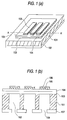
- Fig. 1 typically illustrates an embodiment of the printer head for ink jet recording according to the present invention.
- Fig. 1 (a) is a schematic perspective view of the printer head for ink jet recording according to the present invention.
- Fig. 1 (b) is an enlarged sectional view taken along the line A-A' of Fig. 1 (a).
- the printer head for ink jet recording of the present invention shown in Fig. 1 comprises a single-crystal silicon substrate 101 having a plurality of ink chambers 102; a zirconium oxide layer 103 provided on the single-crystal silicon layer 101 to form the bottom of the ink chambers 102; a piezoelectric element comprising a lower electrode 104 formed on the zirconium oxide layer 103, a piezoelectric layer 105 formed on the lower electrode 104 and an upper electrode 106 formed on the piezoelectric layer 105; and a nozzle plate 107 forming nozzles 108 fused together.
- the ink chambers 102 and nozzles 108 are arranged at a constant pitch.
- a voltage is applied across the lower electrode 104 and the upper electrode 106 to deform the piezoelectric element comprising the lower electrode 104, the piezoelectric layer 105 and the upper electrode 106 and the zirconium oxide layer 103 and hence reduce the volume of the ink chambers 102, making it possible to jet the ink loaded in the ink chambers 102 through the nozzles 108.
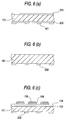
- Fig. 2 is a sectional view illustrating a typical process for the preparation of a printer head for ink jet recording of the present invention involving the steps (a) to (c) of forming a piezoelectric element and ink chambers 102 on a single-crystal silicon substrate 101 by utilizing the volume expansion due to the foregoing crystal phase transition.
- the direction perpendicular to the paper corresponds to the direction of the length of the ink chambers.
- a single-crystal silicon substrate 101 having (110) plane is subjected to wet thermal oxidation at a temperature of from 1,000°C to 1,200°C to form silicon dioxide layers 201 and 202 on both sides thereof, respectively.
- the silicon dioxide layer can also be formed by CVD (chemical vapor deposition method).
- the thickness of the silicon dioxide layers 201 and 202 are not specifically limited but are preferably from 2,000 to 10,000 ⁇ .
- the silicon dioxide layer 201 which acts as an etching stop layer, preferably has a thickness of not less than 2,000 ⁇ taking into account overetching.
- the thickness of the silicon dioxide layer 202, which acts as an etching mask varies with the thickness of the silicon substrate but is preferably from 6,000 to 10,000 ⁇ .
- a zirconium oxide layer 103 described later may be formed directly on the single-crystal silicon substrate 101 without previously oxidizing the single-crystal silicon substrate 101.
- the zirconium oxide layer 103 may be formed directly on the single-crystal silicon substrate 101 after the silicon dioxide layer 201 which has once been formed is etched away.
- a photoresist is formed on the silicon dioxide layer 202 to provide an opening area.
- the silicon dioxide layer 202 is then subjected to patterning with an etching solution (e.g., aqueous solution of hydrofluoric acid and ammonium fluoride) to form an opening area 203.
- an etching solution e.g., aqueous solution of hydrofluoric acid and ammonium fluoride
- the direction of the depth of the opening area 203 i.e., direction perpendicular to the paper is arranged to correspond to ⁇ 1 1 2 ⁇ or ⁇ 1 12 ⁇ direction of the single-crystal silicon substrate 101.
- a zirconium oxide layer 103 is formed on the silicon dioxide layer 201 side of the silicon substrate 101 by a thin film formation process.
- the thickness of the zirconium oxide layer 103 is not specifically limited but is preferably from 0.1 to 2 ⁇ m.
- the upper limit of the thickness of the zirconium oxide layer 103 is determined by the upper limit of residual stress developed after heat treatment effected shortly after the formation of the zirconium oxide layer 103.
- the lower limit of the thickness of the zirconium oxide layer 103 is determined by the upper limit of residual stress developed after heat treatment of the piezoelectric layer.
- thin film formation process is not meant to indicate any specific method so far as it is a thin film formation process commonly used in the production of an electronics device such as printer head for ink jet recording.
- Specific examples of such a thin film formation process include sputtering process, sol-gel process, CVD process, vacuum evaporation process, and hydrothermal process.
- the foregoing zirconium oxide layer 103 is preferably formed, e.g., by a rf-magnetron sputtering process with a sintered zirconium oxide as a sputtering target. Subsequently, the zirconium oxide layer 103 thus formed is subjected to heat treatment at a temperature of 1,050°C to 1,200°C in an atmosphere containing oxygen (particularly air) for 30 minutes to 2 hours. The bending of the substrate supporting the zirconium oxide layer is then measured at room temperature. The residual stress is then calculated from this bending. As a result, the single-crystal silicon substrate is found to receive a stress as small as 0.5 to 3 x 10 -8 N/m 2 from the zirconium oxide layer.
- a process which comprises sputtering in an oxygen atmosphere with a metallic zirconium target may be used to form a zirconium oxide layer.
- sol-gel process or CVD process may be used to form a zirconium oxide layer.
- the zirconium oxide layer 103 is formed by an unstabilized zirconium oxide substantially free of stabilizer so that the crystal structure thereof stays monoclinic at room temperature.
- Zirconium oxide is stabilized when it comprises a stabilizer such as magnesium oxide, calcium oxide, yttrium oxide or cerium oxide incorporated therein in the form of solid solution in an amount of not less than 1 mol-%.
- the process of the present invention utilizing the volume expansion due to the crystal phase transition employs a so-called non-stabilized zirconium oxide (zirconia) rather than so-called stabilized or partially-stabilized zirconium oxide.
- a lower electrode 104 and a piezoelectric layer 105 were laminated on the zirconium oxide layer 103 by a thin-film formation process.
- a section of the laminated material thus obtained is shown in Fig. 2 (a).
- the material of the lower electrode 104 is not specifically limited so far as it is commonly used as an electrode, particularly lower electrode, in the production of an electronics device such as printer head for ink jet recording. It is preferably a stable high melting metal which is little reactive to the temperature of heat treatment of the piezoelectric substance (e.g., PZT) to be formed on the lower electrode. In some detail, it is preferably made of a material comprising platinum or palladium as a main component. The term "as a main component" as used herein is meant to indicate that the content of platinum or palladium is not less than 50% by weight, preferably not less than 80% by weight.
- the thickness of the lower electrode is not specifically limited but is preferably from 1,000 to 10,000 ⁇ . The thickness of the lower electrode is preferably not less than 1,000 ⁇ from the standpoint of sheet resistance. If the thickness of the lower electrode exceeds 10,000 ⁇ , an excessive stress can be disadvantageously applied to the silicon substrate.
- a metal layer made of titanium, tantalum, aluminum, tin, iridium or mixture thereof is preferably formed as an adhesion layer between the zirconium oxide layer 103 and the lower electrode 104 by a thin-film formation process to enhance the adhesivity between the zirconium oxide layer 103 and the lower electrode 104.
- the thickness of the metal layer as adhesion layer is not specifically limited but is preferably from 50 to 1,000 ⁇ .
- the titanium layer as adhesion layer and the platinum layer as lower electrode 104 can be sequentially formed by a d.c. sputtering process.
- a piezoelectric layer 105 is then formed on the lower electrode 104.
- a precursor layer is formed by any one of various thin-film formation processes. Subsequently, the crystallization temperature and the treatment time are properly selected depending on the thin-film formation process used. The material is then subjected to heat treatment under these conditions to convert the precursor to a piezoelectric substance.
- a rapid heating process employing a lamp annealing apparatus (e.g., combination of a first heat treatment for crystallization at 500°C to 700°C for 1 to 5 minutes and a second heat treatment for enhancement of properties at 650°C to 900°C for 1 to 5 minutes) or a heat treatment process by a diffusion furnace commonly used in the preparation of semiconductors which proceeds at a not so particularly rapid rate (e.g., combination of a first heat treatment for crystallization at 500°C to 700°C for 10 minutes to 3 hours and a second heat treatment for enhancement of properties at 650°C to 900°C for 10 minutes to 3 hours) may be mostly used to convert the precursor to the piezoelectric substance.
- a lamp annealing apparatus e.g., combination of a first heat treatment for crystallization at 500°C to 700°C for 1 to 5 minutes and a second heat treatment for enhancement of properties at 650°C to 900°C for 1 to 5 minutes
- a diffusion furnace commonly used in the preparation of semiconductors which
- a sol-gel process is used to form a precursor layer
- the heat treatment conditions are changed depending on the composition of the starting material of sol.
- a rapid heating process employing a lamp annealing apparatus (e.g., combination of a first heat treatment for seed crystal formation at 500°C to 700°C for 1 to 5 minutes and a second heat treatment for crystal growth and enhancement of properties at 650°C to 950°C for 1 to 5 minutes) may be used.
- a piezoelectric layer is obtained during the formation of film.
- the piezoelectric substance employable herein is not specifically limited.
- a ternary PZT (lead zirconate titanate) is preferred because it can provide a piezoelectric substance having a high piezoelectricity.
- a ternary PZT (lead zirconate titanate) represented by the following general formula (1) is preferred: Pb 1+x [(Zr) a (Ti) b (B d B' e ) c ]O 3+x wherein (B and B') represents a combination of a divalent metal ion and a pentavalent metal ion, a combination of a divalent metal ion and a hexavalent metal ion or a combination of a trivalent metal ion and a pentavalent metal ion; and x, a, b, c, d and e satisfy the following relationships: 0 ⁇ x ⁇ 0.3, 0.25 ⁇ a ⁇ 0.55, 0.35
- the trivalent metal ion B is yttrium (Y), iron (Fe), scandium (Sc), ytterbium (Yb), lutetium (Lu), indium (In) or chromium (Cr).
- the pentavalent metal ion B' is niobium (Nb), tantalum (Ta) or antimony (Sb).
- the hexavalent metal ion B' is tungsten (W) or tellurium (Te).
- a ternary PZT which comprises third components, i.e., B and B' in the general formula (1) preferably in an amount of not less than 5 mol-%, more preferably from 5 to 40 mol-% to exhibit a high electrostriction constant may be used.
- the thickness of the piezoelectric layer 105 is not specifically limited but is preferably from 0.5 to 5 ⁇ m. If a metal layer is formed as an adhesion layer between the zirconium oxide layer 103 and the lower electrode 104, the foregoing metal is simultaneously oxidized during the heat treatment of the piezoelectric precursor.
- the piezoelectric substance having higher piezoelectricity can be obtained when the above-described heat treatment temperature in an atmosphere containing oxygen (for crystal growth and/or enhancement of piezoelectricity) is set at a range of from 700 to 900°C, preferably at 800°C.
- the piezoelectric layer 105 is patternwise etched with an etching solution (e.g., aqueous solution of hydrofluoric acid).
- the lower electrode 104 is patternwise etched with an etching solution (e.g., aqueous solution of aqua regia ).
- an upper electrode 106 is formed on the piezoelectric layer 105 by a thin-film formation process.
- the material of the upper electrode 106 is not specifically limited so far as it is commonly used as an electrode, particularly upper electrode, in the production of electronics devices such as printer head for ink jet recording. In some detail, it is preferably made of gold, platinum or aluminum.
- the thickness of the upper electrode is not specifically limited but is preferably from 500 to 5,000 ⁇ .
- an adhesion layer e.g., titanium layer is preferably formed between the piezoelectric layer 105 and the upper electrode 106 by a thin-film formation process to enhance the adhesivity between the piezoelectric layer 105 and the upper electrode 106.
- the thickness of the metal layer as adhesion layer is not specifically limited but is preferably from 50 to 300 ⁇ . After the formation of the upper electrode, a sufficient adhesivity can be obtained without the need of high temperature treatment. Accordingly, the foregoing titanium layer doesn't need to be oxidized.
- the metal layer as adhesion layer and the upper electrode 106 are sequentially formed by a sputtering process, and then patternwise etched with an etching solution (e.g., aqueous solution containing iodine and potassium iodide).
- an etching solution e.g., aqueous solution containing iodine and potassium iodide.
- the structure of the laminated material obtained by patternwise etching the upper electrode 106 formed on the piezoelectric layer 105 is shown in Fig. 2 (b).
- an ion milling process using an inert gas may be employed to obtain the similar laminated material.
- a photosensitive monomer layer for the formation of polyimide is formed as a protective layer 204 for the piezoelectric layer 105 to a thickness of from 0.3 to 5 ⁇ m.
- the protective layer on the upper electrode 106 is then removed by development.
- the laminated material is then subjected to heat treatment at a temperature of from 300°C to 450°C to form a polyimide layer.
- the laminated material is then dipped in an anisotropic etching solution (e.g., 10 to 40% aqueous solution of potassium hydroxide) at a temperature of from 70°C to 90°C to effect an anisotropic etching on the single-crystal silicon substrate 101 at the opening area 203 formed on the silicon dioxide layer 202.
- an anisotropic etching solution e.g., 10 to 40% aqueous solution of potassium hydroxide
- This etching process is arranged such that the face orientation of the single-crystal silicon substrate 101 is (110) and the direction of the length of the opening area 203 is ⁇ 1 1 2 ⁇ or ⁇ 1 12 ⁇ direction. Accordingly, the side wall forming the sides in the length direction of the ink chambers 102 corresponds to (111) plane.
- the ratio of the etching rate on (110) plane to on (111) plane of the single-crystal silicon is about 300 : 1. Accordingly, the degree of side etching on grooves having a depth of 250 ⁇ m in the single-crystal silicon substrate 101 can be restricted to about 1 ⁇ m, making it possible to form ink chambers 102 to a high precision.
- the exposed area of the silicon dioxide layers 202 and 201 is etched away with an etching solution (e.g., aqueous solution of hydrofluoric acid and ammonium fluoride) with the single-crystal silicon substrate 101 kept fixed to the foregoing fixture.
- an etching solution e.g., aqueous solution of hydrofluoric acid and ammonium fluoride
- the zirconium oxide layer 103 is useful as an etching stop layer for the silicon dioxide layer 201 during the formation of the ink chambers 102.
- the yield can be drastically enhanced as compared with the absence of zirconium oxide layer 103.
- non-stabilized zirconium oxide has a higher Young's modulus than zirconium oxide stabilized with magnesium oxide or yttrium oxide.
- the non-stabilized zirconium oxide can provide enhanced ink jetting properties.
- pure zirconium oxide changes its crystal structure with temperature.
- pure zirconium oxide stays monoclinic (also referred to as hexagonal) at a temperature ranging from room temperature to about 1,000°C, tetragonal at a temperature ranging from not lower than about 1,000°C to not higher than about 1,900°C and cubic at a temperature ranging from not lower than about 1,900°C to not higher than about 2,700°C (melting point).
- the heat treatment at 1,050°C to 1,200°C after the formation of the zirconium oxide layer according to the present invention causes the crystal system to change from monoclinic to tetragonal from before to after the formation of the adhesion layer or lower electrode.
- the tetragonal zirconium oxide has a volume of about 3% smaller than that of the monoclinic zirconium oxide. Accordingly, it has been already known that if heat treatment is effected across the monoclinic/tetragonal transition temperature, the resulting volume change is hysteretic with respect to the heat treatment temperature, causing cracking on the crystalline zirconium oxide. In other words, if zirconium oxide as a bulk ceramics is given a heat cycle that causes the crystal structure to be changed, the volume shrinkage accompanies cracking, making it impossible to obtain usable products.
- a bulk ceramics normally comprises magnesium oxide, calcium oxide, yttrium oxide, cerium oxide or the like incorporated therein in the form of solid solution in an amount of from 1 mol-% to 30 mol-% so as to occur always as a high temperature type cubic system. With this composition, a stabilized zirconia which stays cubic at room temperature can be obtained.
- the volume expansion energy of the zirconium oxide is absorbed by the bending of the silicon substrate, making it possible to prevent the cracking of the zirconium oxide layer.
- non-stabilized zirconium oxide undergoes crystal phase transition to monoclinic system and hence volume expansion when cooled from a temperature of not lower than 1,000°C where it stays in the form of thermally stable tetragonal system.
- the single-crystal silicon substrate is subjected to tensile stress from the zirconium oxide layer.
- stabilized zirconia undergoes no crystal phase transition when cooled from a temperature as high as not lower than 1,000°C.
- the single-crystal silicon substrate is subjected to strong compression stress depending only on thermal expansion coefficient (stabilized zirconia has a higher thermal expansion coefficient than silicon).
- heat treatment at a temperature of not lower than 800°C is indispensable.
- the single-crystal silicon substrate is subjected to strong compression stress when cooled from high temperatures regardless of whether or not the stabilized zirconia layer is used.
- the present invention utilizes the foregoing principle.
- the interposition of a so-called non-stabilized zirconium oxide layer between the single-crystal silicon substrate and the lower electrode can reduce the residual stress applied to the single-crystal silicon substrate after the formation of the piezoelectric element and makes it possible to use the zirconium oxide layer formed in the product as a vibrating plate material.
- the silicon substrate and the entire layer structure are subjected to strong mutual stress due to the difference in thermal expansion coefficient between them. If the residual stress in the entire layer structure is great, it is disadvantageous in that if the silicon substrate is etched during the formation of ink chambers, the vibrating plate portion is subjected to great stress change that causes destruction in the vibrating plate portion.
- the residual stress in the entire layer structure is small, making it possible to prevent defects due to stress destruction in the vibrating plate portion (zirconium oxide layer) even during the formation of ink chambers.
- the printer head for ink jet recording is normally subject to stress change in the vibrating plate portion because the vibrating plate portion is allowed to vibrate during the jetting of ink. In this process, if a high residual stress occurs in the vibrating plate portion, the residual stress and the stress developed during the jetting of ink can exceed the limit of breaking stress of the layers reducing the durability of the printer head. However, since the printer head for ink jet recording according to the present invention is less apt to residual stress, the durability of the driving portion including the zirconium oxide layer against displacement operation can be drastically enhanced.
- the printer head for ink jet recording of the present invention can be prepared by a process which comprises, after the formation of a zirconium oxide layer, subjecting the material to heat treatment at a temperature higher than the temperature where the crystal structure of the foregoing zirconium oxide layer changes from monoclinic system to tetragonal system (preferably not lower than 1,050°C, more preferably not lower than 1,150°C).
- the printer head for ink jet recording of the present invention can also be prepared by a process which comprises a step of forming a metallic zirconium layer, and a step of oxidizing the metallic zirconium layer in an atmosphere containing oxygen at a temperature higher than the temperature where the crystal structure of the foregoing zirconium oxide layer is changed from monoclinic system to tetragonal system (preferably not lower than 1,050°C, more preferably not lower than 1,150°C) to convert the metallic zirconium layer to the zirconium oxide layer.
- oxidation reaction allows the formation of a zirconium oxide layer. Accordingly, a dense layer having little pin holes can be obtained.
- the volume expansion due to crystal phase transition as well as the volume expansion due to the conversion of metallic zirconium to zirconium oxide can be utilized in the preparation process.
- the printer head for ink jet recording of the present invention thus obtained comprises a single-crystal silicon substrate pierced with holes; a zirconium oxide layer (preferably having a thickness of from 0.1 to 2 ⁇ m) which is brought into direct contact with the surface of said silicon substrate or a silicon oxide layer on the surface of said silicon substrate so as to cover one end of said holes in said silicon substrate; a lower electrode (preferably having a thickness of from 1,000 to 10,000 ⁇ ) provided on said zirconium oxide layer; optionally an adhesion layer (preferably having a thickness of from 0 to 1,000 ⁇ ) provided interposed between said zirconium oxide layer and said lower electrode; a piezoelectric layer (preferably having a thickness of from 0.5 to 5 ⁇ m) provided on said lower electrode; an upper electrode (preferably having a thickness of from 500 to 5,000 ⁇ ) provided on said piezoelectric layer; and optionally an adhesion layer (preferably having a thickness of from 0 to 300 ⁇ ) provided interposed between said piezoelectric layer and said upper electrode
- the thickness of the foregoing lower electrode be greater than that of the foregoing monoclinic zirconium oxide layer.
- the ratio of the two layers is not less than 1 (particularly from 1 to 10)
- the residual stress occurring on the single-crystal silicon substrate before the formation of ink chambers, the yield in the production of vibrating plate and the durability of the head drive can be enhanced for the same reasons as mentioned above.
- the average crystal grain diameter of the zirconium oxide constituting the foregoing monoclinic zirconium oxide layer is preferably from 500 to 3,000 ⁇ . If the average crystal grain diameter of the zirconium oxide falls within the above defined range, the durability of the head drive can be enhanced.
- the average crystal grain diameter of the zirconium oxide can be properly controlled by changing the heat treatment temperature, the heat treatment time, and/or atmospheric gas in which the heat treatment is effected.
- Fig. 3 typically illustrates an embodiment of the printer head for ink jet recording according to the present invention.
- Fig. 3 (a) is a schematic perspective view of the printer head for ink jet recording according to the present invention.
- Fig. 3 (b) is an enlarged sectional view taken along the line A-A' of Fig. 3 (a).
- the printer head for ink jet recording of the present invention shown in Fig. 3, too, comprises a single-crystal silicon substrate 101 having a plurality of ink chambers 102; a silicon dioxide layer 201 formed on the single-crystal silicon layer 101; a zirconium oxide layer 103 provided on the silicon dioxide layer 201 to form the bottom of the ink chambers 102; a piezoelectric element comprising a lower electrode 104 formed on the zirconium oxide layer 103, a piezoelectric layer 105 formed on the lower electrode 104 and an upper electrode 106 formed on the piezoelectric layer 105; and a nozzle plate 107 forming nozzles 108 fused together.
- the ink chambers 102 and nozzles 108 are arranged at a constant pitch.
- a voltage is applied across the lower electrode 104 and the upper electrode 106 to deform the piezoelectric element comprising the lower electrode 104, the piezoelectric layer 105 and the upper electrode 106 and the zirconium oxide layer 103 and hence reduce the volume of the ink chambers 102, making it possible to jet the ink loaded in the ink chambers 102 through the nozzles 108.
- Fig. 4 is a sectional view illustrating a typical process for the preparation of a printer head for ink jet recording of the present invention involving the steps (a) to (c) of forming a piezoelectric element and ink chambers 102 on a single-crystal silicon substrate 101 by utilizing the volume expansion due to the oxidation of metallic zirconium to zirconium oxide.
- the direction perpendicular to the paper corresponds to the direction of the length of the ink chambers.
- a single-crystal silicon substrate 101 having (110) plane is subjected to wet thermal oxidation at a temperature of from 1,000°C to 1,200°C or CVD to form silicon dioxide layers 201 and 202 on both sides thereof, respectively.
- the thickness of the silicon dioxide layers 201 and 202 is not specifically limited but is preferably from 4,000 to 10,000 ⁇ similarly to the case as mentioned above.
- a metallic zirconium layer 103 described later may be formed directly on the single-crystal silicon substrate 101 without previously oxidizing the single-crystal silicon substrate 101.
- a zirconium oxide layer 103 described later may be formed directly on the single-crystal silicon substrate 101 after the silicon dioxide layer 201 which has once been formed is removed by etching or the like.
- a photoresist is formed on both sides of the silicon dioxide layers 201 and 202 by an ordinary photolithographic process to form a desired pattern on the photoresist on the silicon dioxide layer 202.
- the substrate thus obtained is then dipped in an etching solution (e.g., aqueous solution containing hydrofluoric acid and ammonium fluoride) so that the silicon dioxide layer 202 is patternwise etched to form an opening area 203.
- an etching solution e.g., aqueous solution containing hydrofluoric acid and ammonium fluoride
- the direction of the length of the opening area 203 i.e., the direction perpendicular to the paper corresponds to ⁇ 1 1 2 ⁇ or ⁇ 1 12 ⁇ direction of the single-crystal silicon substrate 101.
- the substrate thus obtained is then dipped in a stripping agent (e.g., sulfuric acid) at a temperature of from 80°C to 90°C to peel the photoresist off the substrate.
- a metallic zirconium layer 103 is then formed on the silicon dioxide layer 201 side of the substrate by a thin-film formation process, particularly d.c. sputtering process.
- the thickness of the metallic zirconium layer is not specifically limited so far as the volume expansion due to the conversion of metallic zirconium to zirconium oxide conforms to the objects of the present invention. In particular, if the process for the oxidation of metallic zirconium to zirconium oxide is effected before the formation of piezoelectric layer, the thickness of the metallic zirconium layer is not restricted.
- the thickness of the metallic zirconium layer is preferably from about 50 ⁇ to about 300 ⁇ .
- a lower electrode 104 is formed by a thin-film formation process, particularly d.c. sputtering process.
- the thickness of the lower electrode is not specifically limited but is preferably from 0.2 to 2 ⁇ m.
- a metal layer for adhesion as mentioned above may be provided interposed between the metallic zirconium layer 103 and the lower electrode 104 by a thin-film formation process to enhance the adhesivity between the zirconium oxide layer 103 formed by the oxidation of the metallic zirconium layer and the lower electrode 104.
- a piezoelectric precursor layer is laminated on the lower electrode 104.
- This precursor layer is formed by a thin-film formation process as mentioned above.
- the precursor layer may be then subjected to heat treatment under crystallization temperature and processing time conditions which are properly adjusted according to the thin-film formation process used.
- the precursor layer may be converted to a piezoelectric layer 105.
- the metallic zirconium layer 103 is oxidized to a zirconium oxide layer 103 whose thickness is as about twice as that of the metallic zirconium layer 103. If heat treatment is effected in the same manner as above in the absence of metallic zirconium layer 103, the lower electrode 104 is peeled off the silicon dioxide layer 201 during this heat treatment. Further, if heat treatment is effected in the same manner as above in the presence of a metallic titanium layer instead of metallic zirconium layer 103, lead diffused from PZT, if PZT is used as a piezoelectric substance, causes the silicon dioxide layer 201 to be melted, causing the lower electrode to be partly peeled off.
- the zirconium oxide layer 103 acts as an adhesion layer for bonding the lower electrode 104 to the silicon dioxide layer 201. It also acts as a lead diffusion preventive layer. If a metal layer as adhesion layer is provided interposed between the metallic zirconium layer 103 and the lower electrode 104, it is oxidized, too, during the heat treatment.
- an upper electrode 106 is formed on the piezoelectric layer 105 by a thin-film formation process.
- the thickness of the upper electrode 106 is not specifically limited but is preferably from 500 to 5,000 ⁇ .
- a metal layer as adhesion layer may be provided interposed between the piezoelectric layer 105 and the upper electrode 106 to enhance the adhesivity between the piezoelectric layer 105 and the upper electrode 106.
- the metal layer as adhesion layer doesn't need to be oxidized.
- an ordinary photolithographic process and an ion milling process with, e.g., inert gas (e.g., argon gas) may be used to sequentially work the upper electrode 106, the piezoelectric layer 105 and the lower electrode 104 into desired shapes.
- inert gas e.g., argon gas
- a laminated material having a section shown in Fig. 4 (b) can be obtained.
- a patternwise etching with an etching solution may be employed to obtain a similar laminated material.
- a photosensitive monomer layer for the formation of polyimide is formed as a protective layer 204 for the piezoelectric layer 105 to a thickness of from 0.3 to 5 ⁇ m.
- the protective layer on the upper electrode 106 is then removed by development.
- the laminated material is then subjected to heat treatment at a temperature of from 300°C to 450°C to form a polyimide layer.
- the subsequent operation and conditions are the same as that described with reference to the foregoing process utilizing the volume expansion due to the crystal phase transition.
- the material is then protected by a fixture on the piezoelectric element side thereof on which the protective layer 204 has been formed.
- the material is then dipped in an aqueous solution of potassium hydroxide so that single-crystal silicon substrate 101 is subjected to anisotropic etching on the opening area 203 of the silicon dioxide layer 202 to form ink chambers 102.
- the exposed area of the silicon dioxide layers 201 and 202 are etched away with an anisotropic etching solution with the single-crystal silicon substrate 101 kept fixed to the foregoing fixture.
- the zirconium oxide layer 103 formed by the thermal oxidation of the metallic zirconium layer is dense and thus is useful as an etching stop layer for the silicon dioxide layer 201 during the formation of the ink chambers 102.
- the materials of the lower electrode, piezoelectric substance, upper electrode and adhesion layer may be the same as that to be used in the foregoing process utilizing the volume expansion due to the crystal phase transition, respectively.
- the reason why the foregoing process utilizing the volume expansion due to the oxidation of metallic zirconium to zirconium oxide can reduce the stress applied to the foregoing single-crystal silicon substrate on the basis of the difference between the volume change of the single-crystal silicon substrate and the volume change of the lower electrode and piezoelectric layer with the heat treatment is as follows.
- the single-crystal silicon substrate supporting the lower electrode and piezoelectric layer is subjected to heat treatment, the single-crystal silicon substrate and the lower electrode and piezoelectric layer show different degrees of volume expansion and shrinkage due to their different thermal expansion coefficients.
- the single-crystal silicon substrate and the lower electrode and piezoelectric layer are subjected to strong mutual stress.
- the lower electrode can crack due to volume shrinkage, etc.
- a metallic zirconium layer is provided interposed between the single-crystal silicon substrate and the lower electrode.
- the metallic zirconium can be oxidized to a zirconium oxide layer at the same time with the foregoing heat treatment to cause a volume expansion that can cancel the stress produced by the difference between the volume change of the single-crystal silicon substrate and the volume change of the lower electrode and piezoelectric layer.
- the zirconium oxide layer formed in the product as a result of the oxidation has a higher density than the zirconium oxide layer formed directly by the thin-film formation process and thus is even useful as an etching stop layer for the single-crystal silicon substrate or silicon dioxide layer.
- the printer head for ink jet recording of the present invention obtained by the process of the present invention which comprises the simultaneous effectuation of a step of converting a piezoelectric precursor layer to a piezoelectric layer and a step of oxidizing metallic zirconium to zirconium oxide comprises a single-crystal silicon substrate pierced with holes; a zirconium oxide layer which is brought into direct contact with the surface of said silicon substrate or a silicon oxide layer on the surface of said silicon substrate so as to cover one end of said holes in said silicon substrate; a lower electrode provided on said zirconium oxide layer; optionally an adhesion layer provided interposed between said zirconium oxide layer and said lower electrode; a piezoelectric layer provided on said lower electrode; an upper electrode provided on said piezoelectric layer; and optionally an adhesion layer provided interposed between said piezoelectric layer and said upper electrode, wherein the thickness of said zirconium oxide layer ranges from 100 to 600 ⁇ , preferably from 150 to 450 ⁇ .
- the thickness of the zirconium oxide layer falls below 100 ⁇ , the adhesivity between the lower electrode and the zirconium oxide layer is reduced. On the contrary, if the thickness of the zirconium oxide layer exceeds 600 ⁇ , the zirconium oxide layer cannot withstand the volume expansion during oxidation, causing the lower electrode to be peeled off more likely. If the thickness of the zirconium oxide layer falls within the range of from 150 to 450 ⁇ , the probability of the peeling of the lower electrode is drastically reduced. In this case, the zirconium oxide layer doesn't need to be formed by non-stabilized zirconium oxide.
- the thickness of the lower electrode is not specifically limited so far as it allows the lower electrode to act as a vibrating plate but is preferably from 0.2 to 2 ⁇ m.
- the thickness of the piezoelectric layer is not specifically limited so far as it allows the piezoelectric layer to fulfill its function but is preferably from 0.5 to 5 ⁇ m.
- the thickness of the upper electrode is not specifically limited but is preferably from 500 to 5,000 ⁇ .
- the technique of the present invention has been described with reference to printer head for ink jet recording.
- the technique of the present invention can also be generally applied to actuators.
- the present invention also relates to an actuator comprising a single-crystal silicon substrate pierced with holes, a zirconium oxide layer which is brought into direct contact with the surface of said silicon substrate or a silicon oxide layer on the surface of said silicon substrate so as to cover one end of said holes in said silicon substrate, a lower electrode provided on said zirconium oxide layer, a piezoelectric layer provided on said lower electrode, and an upper electrode provided on said piezoelectric layer.
- the actuator according to the present invention can also be used as microphone, sound-producing material (e.g., speaker), vibrator or oscillator, sensor, etc.
- a printer head for ink jet recording according to the present invention was prepared by the method shown in Fig. 2.
- the ink chambers 102 thus formed each had a length of 100 ⁇ m in the direction of arrangement [crosswise direction as viewed on the paper] and a length of 4 mm in the direction of depth [direction perpendicular to the paper].
- the piezoelectric layer was formed on the ink chambers in such an arrangement that its length in the direction of arrangement [crosswise direction as viewed on the paper] was 80 ⁇ m.
- the pitch of the ink chambers in the direction of arrangement was 141 ⁇ m.
- the resolution was 180 dpi (dot per inch).
- a single-crystal silicon substrate 101 having (110) plane was subjected to wet thermal oxidation at a temperature of 1,200°C to form silicon dioxide layers 201 and 202 having a thickness of 8,000 ⁇ on both sides thereof, respectively, at the same time.
- a photoresist was formed on the silicon dioxide layer 202 to form an opening area.
- the silicon dioxide layer 202 was subjected to patterning with an aqueous solution containing hydrofluoric acid and ammonium fluoride to form an opening area 203. This patterning process was arranged such that the length direction of the opening area 203, i.e., direction perpendicular to the paper corresponds to ⁇ 1 1 2 ⁇ direction of the single-crystal silicon substrate 101.
- a zirconium oxide layer 103 having a thickness of 1 ⁇ m was formed on the silicon dioxide layer 201 side of the silicon substrate 101 by a rf-magnetron sputtering process with a sintered product of zirconium oxide as a sputtering target. Thereafter, the material was subjected to heat treatment at a temperature of 1,100°C in the air for 1 hour. The bending of the substrate with a zirconium oxide layer was then measured. From this value, the residual stress was calculated.
- the zirconium oxide layer 103 thus formed was made of a so-called non-stabilized zirconia which doesn't comprise impurities such as magnesium oxide, calcium oxide, yttrium oxide and cerium oxide incorporated therein in the form of solid solution in an amount of not less than 1 mol-% so that its crystal structure stays monoclinic at room temperature.
- a lower electrode 104 and a piezoelectric layer 105 were laminated on the zirconium oxide layer 103 to obtain a laminated material having a section shown in Fig. 2 (a).
- a titanium layer was formed as an adhesion layer interposed between the zirconium oxide layer 103 and the lower electrode 104 to a thickness of 50 ⁇ . Titanium for adhesion layer and platinum for lower electrode 104 were successively deposited by a d.c. sputtering process to a thickness of 50 ⁇ and 2,000 ⁇ , respectively.
- the piezoelectric layer 105 was formed of a ternary PZT [PbZrO 3 -PbTiO 3 -Pb (Mg 1/3 Nb 2/3 )O 3 ] to a thickness of 2 ⁇ m.
- a rf-magnetron sputtering process with a sintered product of PZT as a sputtering target was employed.
- the rf-magnetron sputtering was effected without heating the substrate to form an amorphous PZT precursor layer thereon.
- the material was subjected to rapid heat treatment at a temperature of 650°C for 1 minutes and a temperature of 900°C for 1 minute in an atmosphere of oxygen so that the amorphous PZT precursor layer was crystallized to form a piezoelectric PZT layer.
- the piezoelectric layer 105 was patternwise etched with an aqueous solution of hydrofluoric acid.
- the lower electrode 104 was then patternwise etched with an aqueous solution of aqua regia.
- a titanium layer (thickness: 50 ⁇ ) and a metal layer as upper electrode 106 (thickness: 2,000 ⁇ ) were sequentially formed by a sputtering process.
- the material was then patternwise etched with an aqueous solution of iodine and potassium iodide to have a section shown in Fig. 2 (b).
- a photosensitive monomer layer was formed as a protective layer 204 for the piezoelectric layer 105 to a thickness of 2 ⁇ m.
- the protective layer on the upper electrode 106 was then removed by development.
- the laminated material was then subjected to heat treatment at a temperature of 400°C to form a polyimide layer.
- the material was then dipped in an aqueous solution of potassium hydroxide at a temperature of 80°C while being protected by a polypropylene cylindrical fixture (as shown in Fig.
- the exposed area of the silicon dioxide layers 201 and 202 is etched away with an aqueous solution of hydrofluoric acid and ammonium fluoride with the single-crystal silicon substrate 101 kept fixed to the foregoing fixture.
- the resulting yield in production against the cracking of the zirconium oxide layer 103 as a vibrating plate was as good as 98%.
- the zirconium oxide layer 103 is useful as an etching stop layer for the silicon dioxide layer 201 during the formation of the ink chambers 102.
- the yield in the etching process can be drastically enhanced as compared with the absence of zirconium oxide layer 103.
- the non-stabilized zirconium oxide has a higher Young's modulus than zirconium oxide stabilized with magnesium oxide or yttrium oxide.
- the non-stabilized zirconium oxide can provide enhanced ink jetting properties.
- the zirconium oxide layer was made of a non-stabilized zirconium layer whose crystal structure was monoclinic.
- the zirconium oxide layer was made of a partially-stabilized zirconia layer having yttrium oxide incorporated in the form of solid solution in an amount of 5 mol-%, cracking occurred frequently on the thinner portion (portion formed by the zirconium oxide layer and the lower electrode) during the formation of ink chambers 102 in the single-crystal silicon substrate 101.
- the yield in production was as poor as 30%.
- X-ray diffraction of crystal structure showed that the foregoing partially-stabilized zirconia layer has a monoclinic system and a cubic system in admixture.
- Example 1 The procedure of Example 1 was followed to prepare various printer heads for ink jet recording except that the ratio of the thickness of the zirconium oxide layer 103 to the thickness of the lower electrode 104 (thickness of zirconium oxide layer/thickness of lower electrode) was changed in various ways.
- the residual stress applied to the single-crystal silicon substrate before the formation of ink chambers was measured.
- the yield in the production of vibrating plate was determined.
- the head drive durability test was conducted.
- the thickness of the zirconium oxide layer was changed with the thickness of the lower electrode fixed to 2,000 ⁇ .
- the residual stress was calculated from the measurements of the bending of the single-crystal silicon substrate developed before the formation of ink chambers.
- the yield in the production of vibrating plate was judged by the presence or absence of cracking on the vibrating plate. It is represented by the % ratio of accepted products/total products.
- a pulse voltage of 30 V with a pulse width of 1 msec. was applied to the piezoelectric element 1 x 10 9 times.
- the yield was determined before and after the application of pulse voltage.
- the yield was judged by the presence or absence of the cracking on the lower electrode and the zirconium oxide portion. It is represented by the % ratio of accepted products/total products.
- Example 2 The procedure of Example 1 was followed to prepare various printer heads for ink jet recording except that the average crystal grain diameter of the zirconium oxide constituting the zirconium oxide layer was changed in various ways. These printer heads for ink jet recording were then evaluated for durability of the head drive in the same manner as in Example 2. The results are set forth in Table 2. The crystal grain diameter was changed by properly controlling the heat treatment temperature, heat treatment time, and/or atmospheric gas in which the heat treatment is effected. Average crystal grain diameter of zirconium oxide layer ( ⁇ ) Yield after durability test Judgement 200 2% No Good 400 30% No Good 500 68% Good 1,000 97% Good 3,000 70% Good 5,000 25% No Good
- Example 1 The procedure of Example 1 was followed to prepare various printer heads for ink jet recording except that the temperature of the heat treatment effected after the formation of the zirconium oxide layer was changed in various ways. These printer heads for ink jet recording were then evaluated for durability of the head drive in the same manner as in Example 2. The results are set forth in Table 3. Temperature of heat treatment effected after formation of zirconium oxide layer Yield after durability test Judgement 900°C 7% No Good 1,000°C 32% No Good 1,050°C 85% Good 1,100°C 91% Good 1,150°C 95% Excellent 1,200°C 95% Excellent
- the yield after durability test was relatively good at a heat treatment temperature of not lower than 1,050°C and remarkably good at a heat treatment temperature of not lower than 1,150°C.
- a metallic zirconium layer was formed on the silicon dioxide layer 201 to a thickness of about 5,000 ⁇ by a d.c. sputtering process with metallic zirconium as a sputtering target.
- the oxidation of zirconium begins at about 300°C. All the layers oxidized at the oxidizing temperatures shown in Fig. 4 were monoclinic zirconium oxide layers.
- the oxidizing temperature of metallic zirconium be not lower than 1,050°C. If the oxidizing temperature is not lower than 1,150°C, remarkably excellent results were obtained.
- the zirconium oxide layer formed by thermal oxidation was more dense than that obtained by the process for the preparation of zirconium oxide layer described in Example 1. Thus, this zirconium oxide layer can act as a good etching stop layer during the formation of ink chambers. This zirconium oxide layer also gives a higher Young's modulus that enhances the ink jetting properties.
- a printer head for ink jet recording according to the present invention was prepared by the method shown in Fig. 3.
- the ink chambers 102 thus formed each had a length of 100 ⁇ m in the direction of arrangement [crosswise direction as viewed on the paper] and a length of 4 mm in the direction of depth [direction perpendicular to the paper].
- the piezoelectric layer was formed on the ink chambers in such an arrangement that its length in the direction of arrangement [crosswise direction as viewed on the paper] was 80 ⁇ m.
- the pitch of the ink chambers in the direction of arrangement was 141 ⁇ m.
- the resolution was 180 dpi (dot per inch).
- a single-crystal silicon substrate 101 having a thickness of 220 ⁇ m and having (110) plane was subjected to wet thermal oxidation at a temperature of 1,100°C to form silicon dioxide layers 201 and 202 having a thickness of 0.8 ⁇ m on both sides thereof, respectively, at the same time.
- a photoresist was formed on both sides of the silicon dioxide layers 201 and 202 by an ordinary photolithographic process. A desired pattern was then formed on the photoresist on the silicon dioxide layer 202.
- This substrate was then dipped in an aqueous solution of hydrofluoric acid and ammonium fluoride so that the silicon dioxide layer 202 was patternwise etched to form an opening area 203.
- This etching process was arranged such that the length direction of the opening area 203, i.e., direction perpendicular to the paper corresponds to ⁇ 1 1 2 ⁇ direction of the single-crystal silicon substrate 101.
- This substrate was then dipped in sulfuric acid at a temperature of 80°C to remove the photoresist.
- a metallic zirconium layer 103 was then formed on the silicon dioxide layer 201 side of the silicon substrate 101 to a thickness of 200 ⁇ by a d.c. sputtering process.
- a platinum layer was formed as a lower electrode 104 to a thickness of 0.8 ⁇ m by a d.c. sputtering process.
- a ternary PZT [PbZrO 3 -PbTiO 3 -Pb(Mg 1/3 Nb 2/3 )O 3 ] was deposited as a piezoelectric layer 105 to a thickness of 2 ⁇ m.
- a rf-magnetron sputtering process with a sintered product of PZT as a sputtering target was employed.
- the rf-magnetron sputtering was effected without heating the substrate to form an amorphous PZT precursor layer thereon.
- the material was subjected to heat treatment at a temperature of 750°C for 1 minutes in an atmosphere of oxygen so that the amorphous PZT precursor layer was crystallized to form a piezoelectric PZT layer.
- the metallic zirconium layer 103 was oxidized to a zirconium oxide layer whose thickness was as twice (400 ⁇ ) as that of the metallic zirconium layer 103. Subsequently, a metal was deposited as an upper electrode 106 on the piezoelectric layer 105 to a thickness of 0.1 ⁇ m by a d.c. sputtering process.
- a photosensitive monomer layer was formed as a protective layer 204 for the piezoelectric layer 105 to a thickness of 2 ⁇ m.
- the protective layer on the upper electrode 106 was then removed by development.
- the laminated material was then subjected to heat treatment at a temperature of 400°C to form a polyimide layer.
- the material was then dipped in an aqueous solution of potassium hydroxide at a temperature of 80°C while being protected by the same fixture as used in Example 1 on the piezoelectric element side on which the protective layer 204 had been formed so that the single-crystal silicon substrate 101 was subjected to anisotropic etching on the opening area 203 of the silicon dioxide layer 202 to form ink chambers 102.
- This etching process was arranged such that the face orientation of the single-crystal silicon substrate 101 is (110) and the direction of the length of the opening area 203 is ⁇ 1 1 2 ⁇ direction. Accordingly, the side wall forming the sides in the length direction of the ink chambers 102 corresponds to (111) plane.
- the degree of side etching on grooves having a depth of 220 ⁇ m in the single-crystal silicon substrate 101 could be restricted to about 0.8 ⁇ m.
- the exposed area of the silicon dioxide layers 201 and 202 is etched away with an aqueous solution of hydrofluoric acid and ammonium fluoride with the single-crystal silicon substrate 101 kept fixed to the foregoing fixture.
- a printer head for ink jet recording having a good adhesivity between the silicon substrate and the zirconium oxide layer and between the zirconium oxide layer and the lower electrode and free from layer peeling was prepared.
- the printer head was then subjected to durability test in the same manner as in Example 2.
- the resulting yield in production was as high as not less than 80%.
- a metallic zirconium layer 103 was formed directly on the single-crystal silicon substrate 101 without interposing any silicon dioxide layer as shown in Fig. 5.
- silicon dioxide layers 201 and 202 were formed on both sides of the single-crystal silicon substrate 101 in the same manner as in Example 6.
- a photoresist 401 was patternwise formed only on the silicon dioxide layer 202 by an ordinary photolithographic process.
- the substrate on which the foregoing photoresist had been patternwise formed was then dipped in an aqueous solution of hydrofluoric acid and ammonium fluoride so that the silicon dioxide layer 201 was entirely etched away while the silicon dioxide layer 202 was patternwise etched.
- a zirconium oxide layer 103, a lower electrode 104, a piezoelectric layer 105, and an upper electrode 106 were subsequently formed.
- ink chambers 102 and a protective layer 204 were formed in the same manner as in Example 6 to obtain a structure shown in Fig. 5.
- a printer head for ink jet recording having a good adhesivity between the silicon substrate and the zirconium oxide layer and between the zirconium oxide layer and the lower electrode and free from layer peeling was prepared.
- the printer head was then subjected to durability test in the same manner as in Example 2.
- the resulting yield in production was as high as not less than 80%.
- Example 6 The procedure of Example 6 was followed to prepare elements except that the thickness of the metallic zirconium layer was changed in various ways. The yield of these elements were then evaluated.
- the lower electrode and the piezoelectric layer were formed by depositing platinum and a ternary PZT (same as used in Example 6) to a thickness of 0.8 ⁇ m and 1.5 ⁇ m, respectively.
- the quality of these elements was evaluated by the adhesivity of the lower electrode after the heat treatment for crystallization of PZT.
- the chips which show peeling or floating on the lower electrode were regarded as defective.
- the borderline between acceptance and rejection was a yield of 50%. The results are set forth in Table 5.
- Thickness of metallic zirconium layer ( ⁇ ) Thickness of zirconium oxide layer ( ⁇ ) % Yield Judgement 0 0 0 No Good 25 50 4 No Good 50 100 63 Good 100 200 80 Good 200 400 85 Good 300 600 56 Good 400 800 27 No Good 500 1,000 0 No Good
- the thickness of the metallic zirconium layer was doubled by the heat treatment.
- the results of the foregoing experiment show that the preferred thickness of the zirconium oxide layer ranges from 100 to 600 ⁇ .
- the thickness of the lower electrode was from 0.2 to 2 ⁇ m and the thickness of PZT piezoelectric layer was from 0.5 to 5 ⁇ m.
- the preferred thickness of the zirconium oxide layer was found to range from 100 to 600 ⁇ as mentioned above.
- a structure comprising a silicon dioxide layer was used.
- the same experiment as mentioned above was made on the structure free of silicon dioxide layer shown in Example 7.
- the preferred thickness of the zirconium oxide layer was found to range from 100 to 600 ⁇ .
- Example 8 The procedure of Example 8 was followed to prepare elements except that an adhesion layer was further provided interposed between the metallic zirconium layer and the lower electrode.
- adhesion layers were subjected to X-ray analysis. As a result, it was found that these adhesion layers were all oxides.
- the adhesion layer made of tantalum was found to comprise an alloy of tantalum oxide with lead tantalum oxide produced by the reaction of lead diffused from PZT with part of the tantalum layer.
- iridium was used as a metal for adhesion layer, the resulting adhesivity was particularly high, giving a yield rise of from 7 to 10 points, probably because iridium belongs to the same group as the lower electrode metal, i.e., platinum group.
- the stress applied to the single-crystal silicon substrate due to the difference between the volume change of the single-crystal silicon substrate and the volume change of the lower electrode and the piezoelectric layer with the temperature change due to the heat treatment in the preparation process can be reduced by the volume expansion of said monoclinic zirconium oxide layer due to the crystalline phase transition or the oxidation of zirconium to zirconium oxide.
- the printer head for ink jet recording according to the present invention is insusceptible to cracking on a vibrating plate made of the monoclinic zirconium oxide layer and thus can provide a printer head for ink jet recording having an excellent durability. Further, a piezoelectric thin film element having a high piezoelectricity can be integrally formed, making it possible to a printer head for ink jet recording having excellent ink jetting properties at a low cost.
Claims (24)
- Tête d'imprimante à enregistrement par jets d'encre, comprenant un substrat de silicium monocristallin (101) percé de trous, une couche (103) d'oxyde de zirconium mise en contact direct avec la surface du substrat de silicium (101) ou d'une couche d'oxyde de silicium formée à la surface du substrat de silicium (101) afin que l'extrémité des trous du substrat de silicium (101) soit couverte, une électrode inférieure (104) placée sur la couche d'oxyde de zirconium (103), une couche piézoélectrique (105) placée sur l'électrode inférieure (104), et une électrode supérieure (106) placée sur la couche piézoélectrique (105).
- Tête d'imprimante à enregistrement par jets d'encre selon la revendication 1, dans laquelle la structure cristalline de la couche d'oxyde de zirconium (103) reste monoclinique aux températures ambiantes.
- Tête d'imprimante à enregistrement par jets d'encre selon la revendication 1 ou 2, dans laquelle l'épaisseur de la couche d'oxyde de zirconium (103) est supérieure à celle de l'électrode inférieure (104).
- Tête d'imprimante à enregistrement par jets d'encre selon l'une quelconque des revendications 1 à 3, dans laquelle le diamètre moyen des grains cristallins de la couche d'oxyde de zirconium (103) est compris entre 50 et 300 nm (500 et 3 000 Å).
- Tête d'imprimante à enregistrement par jets d'encre selon l'une quelconque des revendications précédentes, dans laquelle l'épaisseur de la couche d'oxyde de zirconium (103) est comprise entre 10 et 60 nm (100 à 600 Å).
- Tête d'imprimante à enregistrement par jets d'encre selon l'une quelconque des revendications précédentes, dans laquelle l'épaisseur de la couche piézoélectrique (105) est comprise entre 0,5 et 5 µm.
- Tête d'imprimante à enregistrement par jets d'encre selon l'une quelconque des revendications 1 à 6, dans laquelle la couche piézoélectrique (105) est une couche de titane-zirconate de plomb (PZT).
- Tête d'imprimante à enregistrement par jets d'encre selon la revendication 7, dans laquelle la couche piézoélectrique (105) est une couche de titanate-zirconate de plomb ternaire (PZT) contenant un troisième ingrédient en quantité qui n'est pas inférieure à 5 mol%.
- Tête d'imprimante à enregistrement par jets d'encre selon l'une quelconque des revendications 1 à 8, dans laquelle l'électrode inférieure (104) est formée d'un matériau contenant du platine ou du palladium comme ingrédient principal.
- Tête d'imprimante à enregistrement par jets d'encre selon l'une quelconque des revendications 1 à 9, comprenant en outre une couche d'adhérence placée entre la couche d'oxyde de zirconium (103) et l'électrode inférieure (104).
- Tête d'imprimante à enregistrement par jets d'encre selon la revendication 10, dans laquelle la couche d'adhérence est formée d'un oxyde métallique.
- Tête d'imprimante à enregistrement par jets d'encre selon la revendication 11, dans laquelle l'oxyde métallique est l'oxyde de titane, l'oxyde de tantale, l'oxyde d'aluminium, l'oxyde d'étain, l'oxyde de plomb et de tantale, l'oxyde d'iridium ou un de leurs mélanges.
- Tête d'imprimante à enregistrement par jets d'encre selon l'une quelconque des revendications 1 à 12, dans laquelle l'électrode inférieure (104), la couche piézoélectrique (105) et l'électrode supérieure (106) ont été réalisées par un procédé de formation de couches minces.
- Procédé de préparation d'une tête d'imprimante à enregistrement par jets d'encre selon l'une des revendications 1 à 13, qui comprend la formation d'une couche d'oxyde de zirconium sur un substrat de silicium monocristallin ou sur la couche d'oxyde de silicium placée à la surface du substrat, afin que soit réduite la contrainte appliquée au substrat de silicium monocristallin et due à la différence entre le changement de volume du substrat de silicium monocristallin et le changement de volume de l'électrode inférieure et de la couche piézoélectrique lors d'un changement de température d'une température élevée à une température ambiante au cours de l'opération de préparation par dilatation en volume de la couche d'oxyde de zirconium due à la transition de phase cristalline ou à l'oxydation du zirconium de l'oxyde de zirconium.
- Procédé de préparation d'une tête d'imprimante à enregistrement par jets d'encre comprenant un substrat de silicium monocristallin percé de trous, une couche d'oxyde de zirconium monoclinique qui est mise en contact direct avec la surface du substrat de silicium ou d'une couche d'oxyde de silicium placée à la surface du substrat de silicium afin que l'extrémité des trous du substrat de silicium soit couverte, une électrode inférieure placée sur la couche d'oxyde de silicium, une couche piézoélectrique disposée sur l'électrode inférieure, et une électrode supérieure placée sur la couche piézoélectrique, le procédé comprenant, après la formation de la couche d'oxyde de zirconium, une étape dans laquelle le matériau, c'est-à-dire le substrat ayant la couche d'oxyde de zirconium, subit un traitement thermique à une température supérieure à la température à laquelle la structure cristalline de la couche d'oxyde de zirconium passe d'une structure tétragonale à une structure monoclinique.
- Procédé de préparation d'une tête d'imprimante à enregistrement par jets d'encre comprenant un substrat de silicium monocristallin percé de trous, une couche d'oxyde de zirconium monoclinique qui est mise en contact direct avec la surface du substrat de silicium ou d'une couche d'oxyde de silicium placée à la surface du substrat de silicium afin qu'une extrémité des trous du substrat de silicium soit couverte, une électrode inférieure placée sur la couche d'oxyde de zirconium, une couche piézoélectrique disposée sur l'électrode inférieure, et une électrode supérieure placée sur la couche piézoélectrique, le procédé comprenant une étape de formation d'une couche de zirconium métallique et une étape d'application au matériau, c'est-à-dire au substrat ayant la couche de zirconium métallique, d'un traitement thermique à une température supérieure à la température à laquelle la structure cristalline de la couche d'oxyde de zirconium passe d'une structure tétragonale à une structure monoclinique en atmosphère contenant de l'oxygène afin que la couche de zirconium métallique se transforme en couche d'oxyde de zirconium.
- Procédé de préparation selon la revendication 15 ou 16, dans lequel la température de traitement thermique n'est pas inférieure à 1 050 °C et de préférence à 1 150 °C.
- Procédé de préparation selon l'une quelconque des revendications 15 à 17, comprenant en outre une étape de formation d'une couche d'un précurseur de matériau piézoélectrique de titanate-zirconate de plomb (PZT) sur l'électrode inférieure, et une couche d'application d'un traitement thermique au matériau à une température qui n'est pas inférieure à 650 °C dans une atmosphère contenant de l'oxygène afin que la couche du précurseur de matériau piézoélectrique de titanate-zirconate de plomb (PZT) se transforme en couche piézoélectrique de titanate-zirconate de plomb (PZT).
- Procédé de préparation selon l'une quelconque des revendications 15 à 17, comprenant en outre une étape de formation d'une couche de précurseur de matériau piézoélectrique de titanate-zirconate de plomb ternaire (PZT) contenant un troisième ingrédient en quantité qui n'est pas inférieure à 5 mol% sur l'électrode inférieure, et une étape d'application au matériau d'un traitement thermique à une température qui n'est pas inférieure à 700 °C, en atmosphère contenant de l'oxygène, afin que la couche de précurseur de matériau piézoélectrique de titanate-zirconate de plomb (PZT) soit transformée en une couche piézoélectrique de titanate-zirconate de plomb (PZT).
- Procédé de préparation d'une tête d'imprimante à enregistrement par jets d'encre comprenant un substrat de silicium monocristallin percé de trous, une couche d'oxyde de zirconium ayant une épaisseur comprise entre 10 et 60 nm (100 à 600 Å) qui est mise en contact direct avec la surface du substrat de silicium ou d'une couche d'oxyde de silicium placée à la surface du substrat de silicium, afin qu'une extrémité des trous du substrat de silicium soit couverte, une électrode inférieure placée sur la couche d'oxyde de zirconium, une couche piézoélectrique placée sur l'électrode inférieure, et une électrode supérieure placée sur la couche piézoélectrique, le procédé comprenant une étape de formation d'une couche de zirconium métallique directement sur le substrat monocristallin ou sur une couche d'oxyde de silicium placée sur le substrat de silicium, une étape de formation d'une électrode inférieure sur la couche de zirconium métallique, une étape de formation d'une couche de précurseur de matériau piézoélectrique de titanate-zirconate de plomb (PZT) sur l'électrode inférieure par un procédé de formation de couches minces, et une étape de traitement du substrat sur lequel a été formée la couche de précurseur de matériau piézoélectrique de titanate-zirconate de plomb (PZT) par un traitement thermique en atmosphère contenant de l'oxygène, afin que la couche de précurseur de matériau piézoélectrique de titanate-zirconate de plomb (PZT) se transforme en une substance piézoélectrique cristalline de titanate-zirconate de plomb (PZT) avec transformation de la couche de zirconium métallique en couche d'oxyde de zirconium.
- Procédé de préparation selon la revendication 20, dans lequel l'étape de formation de la couche de zirconium métallique est suivie d'une étape de formation d'une couche métallique comme couche d'adhérence sur la couche de zirconium métallique, et par une étape de formation d'une électrode inférieure sur la couche métallique.
- Procédé de préparation selon la revendication 21, dans lequel la couche métallique destinée à la couche d'adhérence est une couche formée de titane, de tantale, d'aluminium, d'étain, d'iridium ou d'un de leurs mélanges.
- Procédé de préparation selon l'une quelconque des revendications 20 à 22, dans lequel la température de traitement thermique est comprise entre 650 et 850 °C.
- Organe de manoeuvre comprenant un substrat de silicium monocristallin percé de trous, une couche d'oxyde de zirconium mise en contact direct avec la surface du substrat de silicium ou une couche d'oxyde de silicium placée à la surface du substrat de silicium afin qu'une extrémité des trous formés dans le substrat de silicium soit couverte, une électrode inférieure placée sur la couche d'oxyde de silicium, une couche piézoélectrique formée sur l'électrode inférieure, et une électrode supérieure formée sur la couche piézoélectrique.
Applications Claiming Priority (4)
| Application Number | Priority Date | Filing Date | Title |
|---|---|---|---|
| JP77634/95 | 1995-04-03 | ||
| JP7763495 | 1995-04-03 | ||
| JP721796 | 1996-01-19 | ||
| JP7217/96 | 1996-01-19 |
Publications (2)
| Publication Number | Publication Date |
|---|---|
| EP0736385A1 EP0736385A1 (fr) | 1996-10-09 |
| EP0736385B1 true EP0736385B1 (fr) | 1998-02-25 |
Family
ID=26341483
Family Applications (1)
| Application Number | Title | Priority Date | Filing Date |
|---|---|---|---|
| EP96105380A Expired - Lifetime EP0736385B1 (fr) | 1995-04-03 | 1996-04-03 | Tête d'imprimante à jet d'encre et procédé de fabrication |
Country Status (4)
| Country | Link |
|---|---|
| US (2) | US5933167A (fr) |
| EP (1) | EP0736385B1 (fr) |
| DE (1) | DE69600167T2 (fr) |
| HK (1) | HK1008143A1 (fr) |
Families Citing this family (74)
| Publication number | Priority date | Publication date | Assignee | Title |
|---|---|---|---|---|
| FR2719804B1 (fr) * | 1994-04-26 | 1997-10-17 | Seiko Epson Corp | Tête d'enregistrement à jets d'encre et son procédé de fabrication. |
| US5933167A (en) * | 1995-04-03 | 1999-08-03 | Seiko Epson Corporation | Printer head for ink jet recording |
| JP3503386B2 (ja) * | 1996-01-26 | 2004-03-02 | セイコーエプソン株式会社 | インクジェット式記録ヘッド及びその製造方法 |
| US6089701A (en) | 1996-04-10 | 2000-07-18 | Seiko Epson Corporation | Ink jet recording head having reduced stress concentration near the boundaries of pressure generating chambers |
| JP3267151B2 (ja) * | 1996-04-12 | 2002-03-18 | ミノルタ株式会社 | 圧電振動部材およびその製造方法 |
| JP3713921B2 (ja) * | 1996-10-24 | 2005-11-09 | セイコーエプソン株式会社 | インクジェット式記録ヘッドの製造方法 |
| JPH10211701A (ja) * | 1996-11-06 | 1998-08-11 | Seiko Epson Corp | 圧電体素子を備えたアクチュエータ及びインクジェット式記録ヘッド、並びにこれらの製造方法 |
| JP3414227B2 (ja) * | 1997-01-24 | 2003-06-09 | セイコーエプソン株式会社 | インクジェット式記録ヘッド |
| JPH10202874A (ja) * | 1997-01-24 | 1998-08-04 | Seiko Epson Corp | インクジェットプリンタヘッド及びその製造方法 |
| JP3763175B2 (ja) * | 1997-02-28 | 2006-04-05 | ソニー株式会社 | プリンタ装置の製造方法 |
| DK0968011T3 (da) * | 1997-03-27 | 2004-12-20 | Smith & Nephew Inc | Fremgangsmåde til overfladeoxidation af zirkoniumlegeringer og fremstillet produkt |
| DE69839540D1 (de) * | 1997-06-20 | 2008-07-10 | Seiko Epson Corp | Piezoelektrisches Schichtelement, Verfahren zum Herstellen und Tintenstrahldruckkopf |
| US6648453B2 (en) | 1997-07-15 | 2003-11-18 | Silverbrook Research Pty Ltd | Ink jet printhead chip with predetermined micro-electromechanical systems height |
| US6682174B2 (en) | 1998-03-25 | 2004-01-27 | Silverbrook Research Pty Ltd | Ink jet nozzle arrangement configuration |
| US6935724B2 (en) | 1997-07-15 | 2005-08-30 | Silverbrook Research Pty Ltd | Ink jet nozzle having actuator with anchor positioned between nozzle chamber and actuator connection point |
| US7556356B1 (en) | 1997-07-15 | 2009-07-07 | Silverbrook Research Pty Ltd | Inkjet printhead integrated circuit with ink spread prevention |
| US7468139B2 (en) | 1997-07-15 | 2008-12-23 | Silverbrook Research Pty Ltd | Method of depositing heater material over a photoresist scaffold |
| US7195339B2 (en) | 1997-07-15 | 2007-03-27 | Silverbrook Research Pty Ltd | Ink jet nozzle assembly with a thermal bend actuator |
| US7465030B2 (en) | 1997-07-15 | 2008-12-16 | Silverbrook Research Pty Ltd | Nozzle arrangement with a magnetic field generator |
| US7337532B2 (en) | 1997-07-15 | 2008-03-04 | Silverbrook Research Pty Ltd | Method of manufacturing micro-electromechanical device having motion-transmitting structure |
| US6712453B2 (en) | 1997-07-15 | 2004-03-30 | Silverbrook Research Pty Ltd. | Ink jet nozzle rim |
| US7381340B2 (en) * | 1997-07-15 | 2008-06-03 | Silverbrook Research Pty Ltd | Ink jet printhead that incorporates an etch stop layer |
| US6188415B1 (en) | 1997-07-15 | 2001-02-13 | Silverbrook Research Pty Ltd | Ink jet printer having a thermal actuator comprising an external coil spring |
| WO1999045598A1 (fr) * | 1998-03-04 | 1999-09-10 | Seiko Epson Corporation | Dispositif piezo-electrique, tete d'enregistrement a jet d'encre, procede de fabrication, et imprimante |
| JP3379479B2 (ja) * | 1998-07-01 | 2003-02-24 | セイコーエプソン株式会社 | 機能性薄膜、圧電体素子、インクジェット式記録ヘッド、プリンタ、圧電体素子の製造方法およびインクジェット式記録ヘッドの製造方法、 |
| DE19859914A1 (de) * | 1998-07-22 | 2000-02-03 | Samsung Electro Mech | Verfahren zum Herstellen eines Aktuators für einen Tintenstrahldruckkopf |
| US6290339B1 (en) * | 1998-07-22 | 2001-09-18 | Eastman Kodak Company | Method of directing fluid between a reservoir and a micro-orifice manifold |
| US6291345B1 (en) * | 1998-07-27 | 2001-09-18 | Honeywell International Inc. | Controlled-stress stable metallization for electronic and electromechanical devices |
| US6502928B1 (en) * | 1998-07-29 | 2003-01-07 | Seiko Epson Corporation | Ink jet recording head and ink jet recording apparatus comprising the same |
| US6402304B1 (en) * | 1998-08-12 | 2002-06-11 | Seiko Epson Corporation | Piezoelectric actuator, ink jet printing head, printer, method for manufacturing piezoelectric actuator, and method for manufacturing ink jet printing head |
| JP3517876B2 (ja) * | 1998-10-14 | 2004-04-12 | セイコーエプソン株式会社 | 強誘電体薄膜素子の製造方法、インクジェット式記録ヘッド及びインクジェットプリンタ |
| US6594875B2 (en) * | 1998-10-14 | 2003-07-22 | Samsung Electro-Mechanics Co. | Method for producing a piezoelectric/electrostrictive actuator |
| US6254223B1 (en) * | 1998-10-21 | 2001-07-03 | Samsung Electro-Mechanics Co., Ltd | Ink jet printer head actuator and manufacturing method thereof |
| JP3328609B2 (ja) * | 1998-12-30 | 2002-09-30 | 三星電子株式会社 | インクジェットプリンタヘッドアクチュエータ及びその製造方法 |
| KR100289606B1 (ko) * | 1999-01-25 | 2001-05-02 | 이형도 | 잉크젯 프린트헤드용 챔버판의 패터닝방법과 그에 의해 제조되는 액츄에이터 |
| WO2000071345A1 (fr) * | 1999-05-24 | 2000-11-30 | Matsushita Electric Industrial Co. Ltd. | Tete a jet d'encre et son procede de production |
| JP3389987B2 (ja) | 1999-11-11 | 2003-03-24 | セイコーエプソン株式会社 | インクジェット式記録ヘッド及びその製造方法 |
| JP2001171133A (ja) * | 1999-12-10 | 2001-06-26 | Samsung Electro Mech Co Ltd | インクジェットプリンタヘッドの製造方法 |
| EP1504903B1 (fr) * | 1999-12-24 | 2007-03-07 | Fuji Photo Film Co., Ltd. | Méthode de production de tête à jet d'encre |
| WO2001075985A1 (fr) * | 2000-03-30 | 2001-10-11 | Fujitsu Limited | Actionneur piezoelectrique, son procede de fabrication et tete a jet d'encre dotee de cet actionneur |
| JP3796394B2 (ja) * | 2000-06-21 | 2006-07-12 | キヤノン株式会社 | 圧電素子の製造方法および液体噴射記録ヘッドの製造方法 |
| JP3833070B2 (ja) * | 2001-02-09 | 2006-10-11 | キヤノン株式会社 | 液体噴射ヘッドおよび製造方法 |
| JP3661775B2 (ja) * | 2001-02-14 | 2005-06-22 | セイコーエプソン株式会社 | インクジェット式記録ヘッドの製造方法 |
| US6903491B2 (en) * | 2001-04-26 | 2005-06-07 | Matsushita Electric Industrial Co., Ltd. | Piezoelectric element, actuator, and inkjet head |
| TW506908B (en) * | 2001-09-06 | 2002-10-21 | Nanodynamics Inc | Piezoelectric ink jet print head and the manufacturing process thereof |
| JP3861673B2 (ja) * | 2001-11-30 | 2006-12-20 | ブラザー工業株式会社 | インクジェット記録ヘッド |
| JP3903936B2 (ja) * | 2002-03-18 | 2007-04-11 | セイコーエプソン株式会社 | 圧電素子、圧電アクチュエータ、及び、液体噴射ヘッド |
| KR100519764B1 (ko) * | 2003-03-20 | 2005-10-07 | 삼성전자주식회사 | 잉크젯 프린트헤드의 압전 액츄에이터 및 그 형성 방법 |
| JP2005035013A (ja) * | 2003-07-15 | 2005-02-10 | Brother Ind Ltd | 液体移送装置の製造方法 |
| JP3975979B2 (ja) * | 2003-07-15 | 2007-09-12 | ブラザー工業株式会社 | 液体移送装置の製造方法 |
| US7562451B2 (en) * | 2003-12-09 | 2009-07-21 | Seiko Epson Corporation | Method of manufacturing actuator device for ink jet head |
| JP2005249645A (ja) * | 2004-03-05 | 2005-09-15 | Matsushita Electric Ind Co Ltd | 角速度センサおよびその製造方法 |
| US7427126B2 (en) * | 2004-08-31 | 2008-09-23 | Brother Kogyo Kabushiki Kaisha | Liquid transport device and method for manufacturing liquid transport device |
| US7473278B2 (en) * | 2004-09-16 | 2009-01-06 | Smith & Nephew, Inc. | Method of surface oxidizing zirconium and zirconium alloys and resulting product |
| US7422315B2 (en) * | 2004-09-21 | 2008-09-09 | Fujifilm Corporation | Liquid ejection head and image forming apparatus comprising same |
| JP4858670B2 (ja) * | 2004-12-20 | 2012-01-18 | セイコーエプソン株式会社 | アクチュエータ装置の製造方法及び液体噴射装置 |
| EP1693907B1 (fr) * | 2005-02-21 | 2010-10-13 | Brother Kogyo Kabushiki Kaisha | Procédé de fabrication d'un actionneur piézoélectrique |
| JP2006239958A (ja) * | 2005-03-01 | 2006-09-14 | Fuji Photo Film Co Ltd | 液体吐出ヘッドの製造方法 |
| US20060255692A1 (en) * | 2005-03-22 | 2006-11-16 | Motohiro Yasui | Piezoelectric Actuator, Ink-Jet Head, Method Of Producing Piezoelectric Actuator, And Method Of Producing Ink-Jet Head |
| JP2007019084A (ja) * | 2005-07-05 | 2007-01-25 | Seiko Epson Corp | 圧電素子の製造方法及び液体噴射ヘッドの製造方法 |
| JP5044902B2 (ja) * | 2005-08-01 | 2012-10-10 | 日立電線株式会社 | 圧電薄膜素子 |
| JP5063892B2 (ja) * | 2005-12-20 | 2012-10-31 | 富士フイルム株式会社 | 液体吐出ヘッドの製造方法 |
| JP5188076B2 (ja) * | 2006-04-03 | 2013-04-24 | キヤノン株式会社 | 圧電素子及びその製造方法、電子デバイス、インクジェット装置 |
| JP4881126B2 (ja) * | 2006-10-25 | 2012-02-22 | 株式会社東芝 | ノズルプレートの製造方法、および液滴吐出ヘッドの製造方法 |
| JP5344120B2 (ja) * | 2007-07-05 | 2013-11-20 | セイコーエプソン株式会社 | アクチュエータ装置及びその製造方法並びに液体噴射ヘッド |
| US7963566B2 (en) * | 2007-11-15 | 2011-06-21 | Ge-Hitachi Nuclear Energy Americas Llc | Apparatus and method for repairing a core spray line pipe weld joint |
| US7963568B2 (en) * | 2007-11-16 | 2011-06-21 | GE-Hitachi Nuclear Energy Americans LLC | Apparatus and method for repairing a core spray line elbow weld joint |
| US8361381B2 (en) | 2008-09-25 | 2013-01-29 | Smith & Nephew, Inc. | Medical implants having a porous coated surface |
| JP2010120270A (ja) * | 2008-11-19 | 2010-06-03 | Seiko Epson Corp | 液体噴射ヘッド、液体噴射装置、アクチュエータ装置及び液体噴射ヘッドの製造方法 |
| JP2010228272A (ja) * | 2009-03-26 | 2010-10-14 | Seiko Epson Corp | 液体噴射ヘッドの製造方法、液体噴射ヘッド及び液体噴射装置 |
| JP2012206824A (ja) * | 2011-03-29 | 2012-10-25 | Fuji Xerox Co Ltd | 内部残留応力算出装置、及びプログラム |
| DE102011109008A1 (de) * | 2011-07-29 | 2013-01-31 | Epcos Ag | Verfahren zur Herstellung eines piezoelektrischen Vielschichtbauelements |
| JP2013201198A (ja) | 2012-03-23 | 2013-10-03 | Ricoh Co Ltd | 電気機械変換素子及びその製造方法、圧電型アクチュエータ、液滴吐出ヘッド、インクジェット記録装置 |
| JP6948763B2 (ja) * | 2015-12-21 | 2021-10-13 | セイコーエプソン株式会社 | 圧電素子応用デバイス |
Family Cites Families (12)
| Publication number | Priority date | Publication date | Assignee | Title |
|---|---|---|---|---|
| US4609427A (en) * | 1982-06-25 | 1986-09-02 | Canon Kabushiki Kaisha | Method for producing ink jet recording head |
| US4789425A (en) * | 1987-08-06 | 1988-12-06 | Xerox Corporation | Thermal ink jet printhead fabricating process |
| US5265315A (en) * | 1990-11-20 | 1993-11-30 | Spectra, Inc. | Method of making a thin-film transducer ink jet head |
| JP2665106B2 (ja) * | 1992-03-17 | 1997-10-22 | 日本碍子株式会社 | 圧電/電歪膜型素子 |
| WO1993022140A1 (fr) * | 1992-04-23 | 1993-11-11 | Seiko Epson Corporation | Tete a jet de liquide et procede de production associe |
| JPH06334140A (ja) * | 1992-12-16 | 1994-12-02 | Ricoh Co Ltd | 強誘電体材料および該材料を用いた半導体メモリ、光記録媒体ならびに微小変位制御素子 |
| JP3120260B2 (ja) * | 1992-12-26 | 2000-12-25 | 日本碍子株式会社 | 圧電/電歪膜型素子 |
| JPH06297720A (ja) * | 1993-04-15 | 1994-10-25 | Seiko Epson Corp | インクジェット記録ヘッドの製造方法 |
| EP0636593B1 (fr) * | 1993-07-27 | 1998-09-30 | Ngk Insulators, Ltd. | Structure d'un diaphragme en zircone, procédé de sa fabrication, et élément à couches piézoélectriques/électrostrictif à cette structure d'un diaphragme en zircone |
| US5376875A (en) * | 1993-12-03 | 1994-12-27 | Motorola, Inc. | Battery charger status monitor circuit and method therefor |
| US5493320A (en) * | 1994-09-26 | 1996-02-20 | Lexmark International, Inc. | Ink jet printing nozzle array bonded to a polymer ink barrier layer |
| US5933167A (en) * | 1995-04-03 | 1999-08-03 | Seiko Epson Corporation | Printer head for ink jet recording |
-
1996
- 1996-04-03 US US08/627,065 patent/US5933167A/en not_active Expired - Lifetime
- 1996-04-03 DE DE69600167T patent/DE69600167T2/de not_active Expired - Lifetime
- 1996-04-03 EP EP96105380A patent/EP0736385B1/fr not_active Expired - Lifetime
-
1997
- 1997-05-20 US US08/859,370 patent/US5802686A/en not_active Expired - Lifetime
-
1998
- 1998-07-07 HK HK98108928A patent/HK1008143A1/xx not_active IP Right Cessation
Also Published As
| Publication number | Publication date |
|---|---|
| DE69600167D1 (de) | 1998-04-02 |
| DE69600167T2 (de) | 1998-10-22 |
| US5802686A (en) | 1998-09-08 |
| EP0736385A1 (fr) | 1996-10-09 |
| HK1008143A1 (en) | 1999-04-30 |
| US5933167A (en) | 1999-08-03 |
Similar Documents
| Publication | Publication Date | Title |
|---|---|---|
| EP0736385B1 (fr) | Tête d'imprimante à jet d'encre et procédé de fabrication | |
| US5719607A (en) | Liquid jet head | |
| US7478558B2 (en) | Piezoelectric element, ink jet head, angular velocity sensor, method for manufacturing the same, and ink jet recording apparatus | |
| US7312558B2 (en) | Piezoelectric element, ink jet head, angular velocity sensor, and ink jet recording apparatus | |
| EP0928033B1 (fr) | Elément à couche mince piézoélectrique, procédé de fabrication, et tête d'enregistrement à jet d'encre utilisant cet élément à couche mince piézoélectrique | |
| EP1560278B1 (fr) | Elément diélectrique, élément piézoélectrique, tête à jet d'encre et méthode de produire la tête | |
| US6969157B2 (en) | Piezoelectric element, ink jet head, angular velocity sensor, method for manufacturing the same, and ink jet recording apparatus | |
| EP0691693B1 (fr) | Dispositif piézo-électrique à couche mince et tête d'enregistrement à jet d'encre comportant ce dispositif | |
| US5984458A (en) | Piezoelectric thin-film element and ink-jet recording head using the same | |
| EP0747976B1 (fr) | Element piezo-electrique a couche mince, son procede de preparation et tete d'ecriture a jet d'encre produite a l'aide dudit element | |
| JP3381473B2 (ja) | 液体噴射ヘッド | |
| JP3582550B2 (ja) | インクジェット記録用プリンタヘッドの製造方法 | |
| US7193756B2 (en) | Piezoelectric element, method for fabricating the same, inkjet head, method for fabricating the same, and inkjet recording apparatus | |
| JP3734176B2 (ja) | インクジェット記録用プリンタヘッドの製造方法及びアクチュエータの製造方法 | |
| JPH07235708A (ja) | 圧電/電歪膜型素子の製造方法 | |
| CN100584995C (zh) | 溅射靶、用于制造溅射靶的方法、溅射装置和液体喷射头 | |
| JP2000015809A (ja) | 圧電アクチュエータ | |
| JP2003188431A (ja) | 圧電素子、インクジェットヘッドおよびそれらの製造方法、並びにインクジェット式記録装置 |
Legal Events
| Date | Code | Title | Description |
|---|---|---|---|
| PUAI | Public reference made under article 153(3) epc to a published international application that has entered the european phase |
Free format text: ORIGINAL CODE: 0009012 |
|
| AK | Designated contracting states |
Kind code of ref document: A1 Designated state(s): CH DE FR GB IT LI NL SE |
|
| 17P | Request for examination filed |
Effective date: 19961113 |
|
| GRAG | Despatch of communication of intention to grant |
Free format text: ORIGINAL CODE: EPIDOS AGRA |
|
| 17Q | First examination report despatched |
Effective date: 19970324 |
|
| GRAG | Despatch of communication of intention to grant |
Free format text: ORIGINAL CODE: EPIDOS AGRA |
|
| GRAH | Despatch of communication of intention to grant a patent |
Free format text: ORIGINAL CODE: EPIDOS IGRA |
|
| GRAH | Despatch of communication of intention to grant a patent |
Free format text: ORIGINAL CODE: EPIDOS IGRA |
|
| GRAA | (expected) grant |
Free format text: ORIGINAL CODE: 0009210 |
|
| AK | Designated contracting states |
Kind code of ref document: B1 Designated state(s): CH DE FR GB IT LI NL SE |
|
| ITF | It: translation for a ep patent filed |
Owner name: BUZZI, NOTARO&ANTONIELLI D'OULX |
|
| REG | Reference to a national code |
Ref country code: CH Ref legal event code: EP |
|
| REF | Corresponds to: |
Ref document number: 69600167 Country of ref document: DE Date of ref document: 19980402 |
|
| ET | Fr: translation filed | ||
| REG | Reference to a national code |
Ref country code: CH Ref legal event code: NV Representative=s name: BOVARD AG PATENTANWAELTE |
|
| PLBE | No opposition filed within time limit |
Free format text: ORIGINAL CODE: 0009261 |
|
| STAA | Information on the status of an ep patent application or granted ep patent |
Free format text: STATUS: NO OPPOSITION FILED WITHIN TIME LIMIT |
|
| 26N | No opposition filed | ||
| REG | Reference to a national code |
Ref country code: GB Ref legal event code: IF02 |
|
| PGFP | Annual fee paid to national office [announced via postgrant information from national office to epo] |
Ref country code: CH Payment date: 20080415 Year of fee payment: 13 |
|
| PGFP | Annual fee paid to national office [announced via postgrant information from national office to epo] |
Ref country code: SE Payment date: 20080408 Year of fee payment: 13 |
|
| REG | Reference to a national code |
Ref country code: CH Ref legal event code: PL |
|
| EUG | Se: european patent has lapsed | ||
| PG25 | Lapsed in a contracting state [announced via postgrant information from national office to epo] |
Ref country code: LI Free format text: LAPSE BECAUSE OF NON-PAYMENT OF DUE FEES Effective date: 20090430 Ref country code: CH Free format text: LAPSE BECAUSE OF NON-PAYMENT OF DUE FEES Effective date: 20090430 |
|
| PG25 | Lapsed in a contracting state [announced via postgrant information from national office to epo] |
Ref country code: SE Free format text: LAPSE BECAUSE OF NON-PAYMENT OF DUE FEES Effective date: 20090404 |
|
| REG | Reference to a national code |
Ref country code: FR Ref legal event code: PLFP Year of fee payment: 20 |
|
| PGFP | Annual fee paid to national office [announced via postgrant information from national office to epo] |
Ref country code: NL Payment date: 20150309 Year of fee payment: 20 |
|
| PGFP | Annual fee paid to national office [announced via postgrant information from national office to epo] |
Ref country code: GB Payment date: 20150401 Year of fee payment: 20 Ref country code: DE Payment date: 20150331 Year of fee payment: 20 |
|
| PGFP | Annual fee paid to national office [announced via postgrant information from national office to epo] |
Ref country code: FR Payment date: 20150408 Year of fee payment: 20 Ref country code: IT Payment date: 20150417 Year of fee payment: 20 |
|
| REG | Reference to a national code |
Ref country code: DE Ref legal event code: R071 Ref document number: 69600167 Country of ref document: DE |
|
| REG | Reference to a national code |
Ref country code: NL Ref legal event code: MK Effective date: 20160402 |
|
| REG | Reference to a national code |
Ref country code: GB Ref legal event code: PE20 Expiry date: 20160402 |
|
| PG25 | Lapsed in a contracting state [announced via postgrant information from national office to epo] |
Ref country code: GB Free format text: LAPSE BECAUSE OF EXPIRATION OF PROTECTION Effective date: 20160402 |