EP0779667A2 - Lichtemittierende Diode mit Kantenemission, Anordnung einer lichtemittierenden Diode mit Kantenemission und Herstellungsverfahren - Google Patents
Lichtemittierende Diode mit Kantenemission, Anordnung einer lichtemittierenden Diode mit Kantenemission und Herstellungsverfahren Download PDFInfo
- Publication number
- EP0779667A2 EP0779667A2 EP96119979A EP96119979A EP0779667A2 EP 0779667 A2 EP0779667 A2 EP 0779667A2 EP 96119979 A EP96119979 A EP 96119979A EP 96119979 A EP96119979 A EP 96119979A EP 0779667 A2 EP0779667 A2 EP 0779667A2
- Authority
- EP
- European Patent Office
- Prior art keywords
- type
- conductive
- emitting
- semiconductor substrate
- face light
- Prior art date
- Legal status (The legal status is an assumption and is not a legal conclusion. Google has not performed a legal analysis and makes no representation as to the accuracy of the status listed.)
- Withdrawn
Links
- 238000004519 manufacturing process Methods 0.000 title claims description 42
- 238000000034 method Methods 0.000 title description 23
- 238000009792 diffusion process Methods 0.000 claims abstract description 147
- 239000000758 substrate Substances 0.000 claims abstract description 122
- 239000004065 semiconductor Substances 0.000 claims abstract description 93
- 230000002265 prevention Effects 0.000 claims description 49
- 238000005530 etching Methods 0.000 claims description 22
- 229910001218 Gallium arsenide Inorganic materials 0.000 claims description 13
- 239000012535 impurity Substances 0.000 claims description 11
- 229910052581 Si3N4 Inorganic materials 0.000 claims description 6
- VYPSYNLAJGMNEJ-UHFFFAOYSA-N Silicium dioxide Chemical compound O=[Si]=O VYPSYNLAJGMNEJ-UHFFFAOYSA-N 0.000 claims description 6
- PNEYBMLMFCGWSK-UHFFFAOYSA-N aluminium oxide Inorganic materials [O-2].[O-2].[O-2].[Al+3].[Al+3] PNEYBMLMFCGWSK-UHFFFAOYSA-N 0.000 claims description 6
- 239000000463 material Substances 0.000 claims description 6
- HQVNEWCFYHHQES-UHFFFAOYSA-N silicon nitride Chemical compound N12[Si]34N5[Si]62N3[Si]51N64 HQVNEWCFYHHQES-UHFFFAOYSA-N 0.000 claims description 6
- 229910052814 silicon oxide Inorganic materials 0.000 claims description 6
- 230000003287 optical effect Effects 0.000 claims description 4
- JBRZTFJDHDCESZ-UHFFFAOYSA-N AsGa Chemical compound [As]#[Ga] JBRZTFJDHDCESZ-UHFFFAOYSA-N 0.000 description 10
- 238000000605 extraction Methods 0.000 description 9
- 238000003491 array Methods 0.000 description 8
- 230000015572 biosynthetic process Effects 0.000 description 6
- 238000004544 sputter deposition Methods 0.000 description 6
- 238000001771 vacuum deposition Methods 0.000 description 6
- 238000005229 chemical vapour deposition Methods 0.000 description 4
- 238000010586 diagram Methods 0.000 description 4
- 238000000059 patterning Methods 0.000 description 4
- KRKNYBCHXYNGOX-UHFFFAOYSA-N citric acid Chemical compound OC(=O)CC(O)(C(O)=O)CC(O)=O KRKNYBCHXYNGOX-UHFFFAOYSA-N 0.000 description 3
- 238000011109 contamination Methods 0.000 description 3
- 230000007547 defect Effects 0.000 description 3
- 239000005360 phosphosilicate glass Substances 0.000 description 3
- 238000001039 wet etching Methods 0.000 description 3
- 229910000980 Aluminium gallium arsenide Inorganic materials 0.000 description 2
- KRHYYFGTRYWZRS-UHFFFAOYSA-N Fluorane Chemical compound F KRHYYFGTRYWZRS-UHFFFAOYSA-N 0.000 description 2
- MHAJPDPJQMAIIY-UHFFFAOYSA-N Hydrogen peroxide Chemical compound OO MHAJPDPJQMAIIY-UHFFFAOYSA-N 0.000 description 2
- NBIIXXVUZAFLBC-UHFFFAOYSA-N Phosphoric acid Chemical compound OP(O)(O)=O NBIIXXVUZAFLBC-UHFFFAOYSA-N 0.000 description 2
- QAOWNCQODCNURD-UHFFFAOYSA-N Sulfuric acid Chemical compound OS(O)(=O)=O QAOWNCQODCNURD-UHFFFAOYSA-N 0.000 description 2
- 238000010521 absorption reaction Methods 0.000 description 2
- 229910052782 aluminium Inorganic materials 0.000 description 2
- XAGFODPZIPBFFR-UHFFFAOYSA-N aluminium Chemical compound [Al] XAGFODPZIPBFFR-UHFFFAOYSA-N 0.000 description 2
- 230000007423 decrease Effects 0.000 description 2
- 238000001312 dry etching Methods 0.000 description 2
- 229910052698 phosphorus Inorganic materials 0.000 description 2
- 239000011574 phosphorus Substances 0.000 description 2
- 238000000206 photolithography Methods 0.000 description 2
- 238000005498 polishing Methods 0.000 description 2
- 239000012808 vapor phase Substances 0.000 description 2
- 239000002966 varnish Substances 0.000 description 2
- NCGICGYLBXGBGN-UHFFFAOYSA-N 3-morpholin-4-yl-1-oxa-3-azonia-2-azanidacyclopent-3-en-5-imine;hydrochloride Chemical compound Cl.[N-]1OC(=N)C=[N+]1N1CCOCC1 NCGICGYLBXGBGN-UHFFFAOYSA-N 0.000 description 1
- 241001046947 Ectropis obliqua Species 0.000 description 1
- 229910000147 aluminium phosphate Inorganic materials 0.000 description 1
- 230000015556 catabolic process Effects 0.000 description 1
- 230000002950 deficient Effects 0.000 description 1
- -1 for example Substances 0.000 description 1
- 239000011810 insulating material Substances 0.000 description 1
- 238000009413 insulation Methods 0.000 description 1
- 230000001681 protective effect Effects 0.000 description 1
- JBQYATWDVHIOAR-UHFFFAOYSA-N tellanylidenegermanium Chemical compound [Te]=[Ge] JBQYATWDVHIOAR-UHFFFAOYSA-N 0.000 description 1
- 238000002834 transmittance Methods 0.000 description 1
- 239000011701 zinc Substances 0.000 description 1
Images







Classifications
-
- H—ELECTRICITY
- H10—SEMICONDUCTOR DEVICES; ELECTRIC SOLID-STATE DEVICES NOT OTHERWISE PROVIDED FOR
- H10H—INORGANIC LIGHT-EMITTING SEMICONDUCTOR DEVICES HAVING POTENTIAL BARRIERS
- H10H20/00—Individual inorganic light-emitting semiconductor devices having potential barriers, e.g. light-emitting diodes [LED]
- H10H20/80—Constructional details
- H10H20/81—Bodies
- H10H20/819—Bodies characterised by their shape, e.g. curved or truncated substrates
-
- H—ELECTRICITY
- H10—SEMICONDUCTOR DEVICES; ELECTRIC SOLID-STATE DEVICES NOT OTHERWISE PROVIDED FOR
- H10H—INORGANIC LIGHT-EMITTING SEMICONDUCTOR DEVICES HAVING POTENTIAL BARRIERS
- H10H20/00—Individual inorganic light-emitting semiconductor devices having potential barriers, e.g. light-emitting diodes [LED]
- H10H20/80—Constructional details
- H10H20/81—Bodies
-
- H—ELECTRICITY
- H10—SEMICONDUCTOR DEVICES; ELECTRIC SOLID-STATE DEVICES NOT OTHERWISE PROVIDED FOR
- H10H—INORGANIC LIGHT-EMITTING SEMICONDUCTOR DEVICES HAVING POTENTIAL BARRIERS
- H10H20/00—Individual inorganic light-emitting semiconductor devices having potential barriers, e.g. light-emitting diodes [LED]
- H10H20/80—Constructional details
- H10H20/81—Bodies
- H10H20/819—Bodies characterised by their shape, e.g. curved or truncated substrates
- H10H20/821—Bodies characterised by their shape, e.g. curved or truncated substrates of the light-emitting regions, e.g. non-planar junctions
Definitions
- the present invention relates to an end face light-emitting-type LED (Light Emitting Diode), an end face light-emitting-type LED array, and methods of manufacturing them.
- LED Light Emitting Diode
- LED arrays have been used, for example, as light sources in electrophotographic printers. There is a type of LED array which is know by the name of end face light-emitting-type LED array.
- the end face light-emitting-type LED arrays are formed by dicing a semiconductor wafer having a laminated structure which is composed of an N electrode, an N-type GaAs buffer layer, an N-type AlGaAs layer, a P-type AlGaAs layer and a P electrode.
- the end face was formed by cutting both the P-type region and the N-type layer.
- the end face was formed by cutting both the P-type regions and the N-type layer using a dicing machine and the like.
- the LED array formed by this method only the light emitted from P/N junctions below the P-type regions when viewed from the front of the end face is effectively extracted, so the light intensity emitted from each element was small.
- an end face light-emitting-type LED has a first-conductive-type semiconductor substrate and a second-conductive-type diffusion region formed on a first surface of the first-conductive-type semiconductor substrate so as to have a depth within a predetermined value.
- the first-conductive-type semiconductor substrate has a second surface which meets the first surface at a predetermined angle with the first surface.
- a junction between the first-conductive-type semiconductor substrate and the second-conductive-type diffusion region includes an inclined portion with regard to the first surface in the vicinity of an edge portion of the junction which is on a side of the second surface, and light emits from the junction via the second surface.
- a method of manufacturing an end face light-emitting-type LED which emits light from a junction between a first-conductive-type semiconductor substrate and a second-conductive-type diffusion region.
- the method has the steps of: forming a diffusion prevention film on a first surface of the first-conductive-type semiconductor substrate; forming a first aperture having a predetermined size at a predetermined position in the diffusion prevention film; forming the second-conductive-type diffusion region by diffusing second-conductive-type impurities in the first surface of the first-conductive-type semiconductor substrate via the first aperture; and forming a second surface, which meets the first surface at a predetermined angle, on the first-conductive-type semiconductor substrate.
- the second-conductive-type diffusion region is formed in such a way that the junction between the first-conductive-type semiconductor substrate and the second-conductive-type diffusion region includes an inclined portion with regard to the first surface in the vicinity of an edge portion of the junction which is on a side of the second surface.
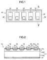
- Fig. 1 is a plan view schematically showing an end face light-emitting-type LED array 10 including a plurality of end face light-emitting-type LEDs according to a first embodiment of the present invention
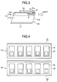
- Fig. 2 is a cross section along a line A-A schematically showing the LED array 10 of Fig. 1
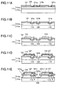
- Fig. 3 is a cross section along a line B-B schematically showing the LED array 10 of Fig. 1.
- the LED array 10 comprises a first-conductive-type semiconductor substrate 11, and a plurality of second-conductive-type diffusion regions 13 formed within a predetermined depth on a first surface 11c of the first-conductive-type semiconductor substrate 11.
- the first-conductive-type is treated as N-type
- second-conductive-type is treated as P-type.
- the N-type semiconductor substrate 11 comprises an N-type gallium arsenic substrate (N-type GaAs substrate) 11a, and an N-type gallium arsenic phosphorus layer (N-type GaAsP layer) 11b epitaxially grown on the N-type GaAs substrate 11a.
- the P-type diffusion regions 13 are P-type gallium arsenic phosphorus regions (P-type GaAsP regions) formed at predetermined intervals (corresponding to the row pitch of the LEDs).
- the LED array 10 comprises a diffusion prevention film 21 having a plurality of apertures 21a, and a plurality of P electrodes 15 connected to the P-type diffusion regions 13 via the apertures 21a respectively, on the N-type semiconductor substrate 11.
- the LED array 10 further comprises an N electrode 17 underneath the N-type semiconductor substrate 11.
- the diffusion prevention film 21 is necessary during manufacture, and has the function of preventing P-type impurities used in forming the P-type GaAsP region 13 from diffusing outside a predetermined region of the N-type semiconductor substrate 11 in the manufacturing process.
- the diffusion prevention film 21 is formed of an insulating material, and has the function of electrically insulating the N-type semiconductor substrate 11 and the P electrodes 15. It may be noted that by forming another insulating film having insulating properties on the diffusion prevention film 21, the occurrence of insulation breakdowns may be reduced.
- the N-type semiconductor substrate 11 comprises a second surface 11d which meets the first surface 11c at an angle ⁇ . Light is radiated via the second surface 11d from each P/N junction 4, which is a boundary between the N-type semiconductor substrate 11 and the P-type diffusion region 13.
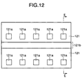
- Fig. 4 is a plan view of a diced LED array (corresponding to Fig. 5F)
- Figs. 5A - 5F are cross sections showing a method of manufacturing the LED array 10 (cross sections taken along a line C-C in Fig. 4).
- the diffusion prevention film 21 is formed on the N-type GaAsP layer 11b of the N-type semiconductor substrate 11, for example, by the vacuum evaporation method, the sputtering method or the CVD method.
- the diffusion prevention film 21 is then patterned by photolithography technique and etching technique so as to form the apertures 21a.
- the diffusion prevention film 21 may be, for example, an alumina film, a silicon nitride film or a silicon oxide film.
- the film thickness may, for example, lie in the range of 50[nm] to 500[nm].
- a diffusion control film 25 is formed on the N-type semiconductor substrate 11 having the diffusion prevention film 21, for example, by the vacuum evaporation method, the sputtering method or the CVD method.
- the diffusion control film 25 may, for example, be an alumina film, a silicon nitride film, a silicon oxide film or a PSG (Phospho Silicate Glass) film.
- the film thickness may, for example, lie in the range of 10[nm] to 300[nm].
- the diffusion control film 25 is provided so that defects, which is made while the diffusion process, on the outermost surface of the N-type semiconductor substrate 11 do not affect the element, and it is completely removed after the diffusion process is complete as described hereafter.
- the P-type diffusion region 13 may be formed without forming the diffusion control film 25, however if the diffusion control film 25 is formed, it reduces defects on the outermost surface due to the diffusion process.
- P-type impurities for example, zinc (Zn) are caused to diffuse via the diffusion control film 25 into the apertures 21a where the N-type semiconductor substrate 11 is not covered by the diffusion prevention film 21, for example, by the vapor phase diffusion method, so as to form the P-type GaAsP region (diffusion region) 13 having a diffusion depth Xj.
- P-type impurities for example, zinc (Zn)
- the diffusion control film 25 is removed, for example, by wet etching method or dry etching method, as shown in Fig. 5B.
- the P electrodes 15 respectively connected to the P-type GaAsP regions 13 are formed by a film forming technique such as the vacuum evaporation method or the sputtering method and fine patterning technique, as shown in Fig. 5C.
- a film forming technique such as the vacuum evaporation method or the sputtering method and fine patterning technique, as shown in Fig. 5C.
- the material of the P electrodes 15 provided that it gives good ohmic contact with the P-type GaAsP regions 13, e.g. aluminum may be used as the P electrodes 15.
- the diffusion prevention film 21 is removed by photolithography-etching from regions 41 which are to be diced between the adjacent LED arrays 10, as shown in Fig. 5D. Dicing may be performed without removing the diffusion prevention film 21 from the regions 41 to be diced, however it is desirable to first remove the diffusion prevention film 21 as otherwise the film may peel and the P electrodes 15 may peel off during dicing.
- the N electrode 17 is formed on the underside of the N-type semiconductor substrate 11 as shown in Fig. 5E.
- the N electrode 17 may be formed after polishing the underside of the N-type semiconductor substrate 11 so as to improve characteristics.
- Removal of the diffusion prevention film 21 from the regions 41 to be diced may be performed prior to formation of the P electrode 15 (Fig. 5C), and removal of the diffusion prevention film 21 from the regions 41 to be diced (Fig. 5D) may also be performed after formation of the N electrode 17 (Fig. 5E).
- the light emitting characteristics and electrical characteristics of the LEDs are then inspected by probing, and the LED arrays are separated into satisfactory and defective products.
- a part between the adjacent LED arrays 10 is obliquely cut by dicing so as to form a second surface (i.e., end face) 11d (Fig. 5F).
- This second surface 11d has a structure such that light obtained from the P/N junction 4, can be effectively extracted on the side of the second surface 11d. More specifically, the position and angle of the second surface 11d are set so that the P/N junction 4 is belt-shaped when viewed from the front of the second surface 11d in the direction parallel to the first surface 11c. It is preferable that the angle ⁇ (see Fig. 3) of the second surface 11d is less than 90° relative to the first surface 11c (i.e. oblique dicing is preferred). However if the belt-shaped light emission radiated from the P/N junction 4 can be used, dicing may be performed such that the angle ⁇ is 90° or more.
- Fig. 6 is a tracing of a photo of a cross section of an LED array specimen which was actually manufactured according to the manufacturing method of the first embodiment.
- the P-type GaAsP regions 13 are formed by diffusing impurities through the diffusion control film 25 from the apertures 21a in the diffusion prevention film 21.
- the P-type diffusion regions 13 are then formed over a wider region than the apertures 21a in the diffusion prevention film 21 due to side diffusion, and its cross section has a diffusion shape 51 as shown by the solid line in Fig. 6.
- the cross section of the P-type diffusion region 13 formed by diffusion may also acquire the diffusion shape 52 or diffusion shape 53.
- a slant angle ⁇ in a cross section of a side diffusion part of the P-type GaAs region 13 according to this embodiment is approximately of the order of 40° , and the dicing end face is also formed so that it has a slant angle ⁇ .
- Fig. 7 is a graph showing a relation between a length Lme from an edge of the aperture 21a in the diffusion prevention film 21 to the chip edge formed by dicing, and an end face light emitting intensity, in the end face light-emitting-type LED according to the first embodiment.
- the vertical axis shows relative light intensity (arbitrary units) and the horizontal axis shows Lme length (relation with the depth Xj of the diffusion region 13).
- the slant angle ⁇ in the cross section of the side diffusion part is approximately 40°
- the distance Lme is approximately 1.2 times the diffusion depth Xj.
- Lme lies within the range of from 0.4 times to 2.4 times Xj (referring to 0.4 Xj, 1.2 Xj and 2.4 Xj in Fig. 6)
- the end face position is therefore set by dicing such that Lme is equal to from 0.4 times to 2.4 times Xj, i.e., so that the following relational expression (1) 0.4 ⁇ Lme / Xj ⁇ 2.4 is satisfied.
- the light intensity extracted from the end face is a maximum when Lme has a length equal to 1.2 times Xj.
- Lme has a length equal to 1.2 times Xj.
- the oblique part 4a of the P/N junction 4 on the end face side is cut by dicing so the light intensity decreases.
- light emitting end faces are formed by dicing and at the same time, arrays are separated (Fig. 5F).
- Good chips are then selected based on probing determination data, and connected to a drive circuit to fabricate a printer head or the like. After the good chips have been incorporated in the head, they are coated with varnish or the like so as to improve light extraction efficiency. The reason for improvement of light extraction efficiency due to the vanish or the like is described below.
- n 1 denotes a refractive index of the substrate
- n 2 denotes a refractive index of the coated film
- d 2 denotes a thickness of the coated film
- ⁇ denotes a wavelength of the extracted light.
- Fig. 8 shows the light intensities extracted from the substrate of the cases when no coated film is provided (solid line), when the coated film having a refractive index n 2 of 1.4 is provided (thin dotted line), and when the coated film having a refractive index of 1.9 is provided (thick dotted line).
- the substrate is a GaAs substrate having a refractive index n 1 of 3.5, and the wavelength of the light extracted from LED is 740 [nm].
- the light intensities shown in Fig. 8 are obtained by calculation.
- Fig. 8 shows that when the coated film having the refractive index n 2 between those (n 1 and n 3 ) of the air and the substrate is provided on the end face of the substrate, there are regions of the film thickness where light extraction efficiency can be increased in comparison with that without the coated film.
- the P/N junction is not cropped out on the second surface 11d, i.e., the condition Lme>1.2Xj is satisfied, since the P/N junctions are not cropped out, the junctions are prevented from contamination, so reliability of the light emitting parts can be increased.
- the light intensity can be increased.
- the light emitted from the P/N junctions 4 as a light emitting parts can be effectively extracted from the end face.
- the light intensity from the end face light emitting LED can be increased.
- the light is extracted from the second surface in the direction parallel to the first surface.
- the LED array 110 comprises a first-conductive-type semiconductor substrate 111, and a plurality of second-conductive-type diffusion regions 113 formed on a first surface 111c of the first-conductive-type semiconductor substrate 111 so as to have a depth within a predetermined value.
- the first-conductive-type is treated as N-type
- the second-conductive-type is treated as P-type in this embodiment, too.
- Fig. 9 is a plan view schematically showing an LED array 110 provided with a plurality of end face light-emitting-type LEDs according to the second embodiment of the present invention.
- Fig. 10 is a cross section along a line D-D schematically showing the LED array 110 of Fig. 9.
- the LED array 110 shown in Fig. 9 and Fig. 10 differs from the LED array 10 shown in Fig. 1 to Fig. 3 insofar as concerns the shape of a second surface 111d which is the light emitting surface of the N-type semiconductor substrate 111.
- the second surface 111d shown in Fig. 9 and Fig. 10 differs in that it comprises lateral walls of a depression formed by etching as compared to the plane formed by dicing in the case of the second surface 11d shown in Fig. 1 to Fig. 3.
- Figs. 11A - 11I are cross sections showing the method of manufacturing the LED array 110 according to the second embodiment
- Fig. 12 is a plan view of Fig. 11B.
- an N-type GaAsP layer 111b is epitaxially grown on an N-type GaAs substrate 111a so that semiconductor substrate 111 comprising the N-type GaAs substrate 111a and the N-type GaAsP layer 111b is obtained.
- the diffusion prevention film 121 is formed on the N-type GaAsP layer 111b of the N-type semiconductor substrate 111, for example, by the vacuum evaporation method, the sputtering method or the CVD method.
- the diffusion prevention film 121 is then patterned by the photolithography technique and the etching technique so as to form the apertures 121a and the apertures 121b.
- the diffusion prevention film 121 may, for example, be an alumina film, a silicon nitride film or a silicon oxide film.
- the film thickness may, for example, lie in the range of 50[nm] to 500[nm].
- a diffusion control film 125 is formed on the N-type semiconductor substrate 111 having the diffusion prevention film 121, for example, by the vacuum evaporation method, the sputtering method or the CVD method.
- the diffusion control film 125 may, for example, be an alumina film, a silicon nitride film, a silicon oxide film or a PSG film.
- the film thickness may, for example, lie in the range of 10[nm] to 300[nm].
- P-type impurities for example, Zn
- P-type impurities are caused to diffuse via the diffusion control film 125 into the apertures 121a and the apertures 121b where the N-type semiconductor substrate 111 is not covered by the diffusion prevention film 121, for example, by the vapor phase diffusion method, so as to form the P-type GaAsP regions 113 and 123 having a diffusion depth Xj.
- the P-type GaAsP regions 113 are regions for forming the P/N junctions 4, and the P-type GaAsP regions 123 are removed by an etching process described hereafter.
- the diffusion control film 125 which is no longer required is removed, for example, by the wet etching method or the dry etching method, so as to give the shape shown in Fig. 11B and Fig. 12.
- the P electrodes 115 connected to the P-type GaAsP regions 113 are formed by the film forming technique such as the vacuum evaporation method or the sputtering method and the fine patterning technique, as shown in Fig. 11C.
- the material of the P electrode 115 there is no particular limitation on the material of the P electrode 115 provided that it gives good ohmic contact with the P-type GaAsP region 113, e.g. aluminum may be used as the material of the P electrodes 115.
- an etching mask 127 which covers regions other than regions where depressions are to be formed which should not be etched during the eaves-like edge removal etching, and which assists the formation of depressions, is formed on the specimen as shown in Fig. 11D.
- the P-type GaAsP region 123 and the N-type semiconductor substrate 111 in its vicinity are removed by etching so as to form a predetermined depression 128 as shown in Fig. 11E.
- This depression 128 is formed so as to exceed the depth of the P/N junction 4 comprising the P-type diffusion region 113 and the N-type semiconductor substrate 111.
- the etching mask 127 may be formed, for example, of the photo-resist.
- the etching may be wet etching using an aqueous phosphoric acid : hydrogen peroxide system, a citric acid system, a hydrofluoric acid system or a sulfuric acid system.
- the eaves-like edges 121c in the diffusion prevention film 121 which functioned as a mask during formation of the depression 128 are removed as shown in Fig. 11F.
- the etching mask 127 used to assist formation of the depression 128 is removed by a suitable method as shown in Fig. 11G.
- the same material may be used for the etching mask 127 as that of the diffusion prevention film 121, however etching may be performed using also a photo-resist or another film as mask.
- the N electrode 117 is formed underneath the N-type semiconductor substrate 111 as shown in Fig. 11H, however the N electrode 117 may be formed after polishing the underside of the N-type semiconductor substrate 111 to improve characteristics.
- the N-type semiconductor substrate 111 is cut from the underside of the depression 128 by dicing so as to separate arrays as shown in Fig. 11I. Good chips are selected based on probing determination data, and connected to a drive circuit to fabricate a printer head.
- the second surface 111d which emits light is formed by etching, hence high precision is not required of the dicing shown in Fig. 11I and manufacture is facile.
- a protective film may also be coated on the end face (second face 111d) of good chips so as to improve emitted light extraction efficiency. It should be noted that the light is extracted from the second surface and advances in a direction parallel to the first surface.
- Figs. 11A - 11c show the case that the apertures 121a and 121b are formed by the same patterning process, however the aperture 121b may be formed by another patterning process after the process shown in Fig. 11B or the process shown in Fig. 11c.
- Fig. 13 is a tracing of a photo of a cross section of an LED array specimen which was actually manufactured.
- the P-type GaAsP regions 113 are formed by diffusing the impurities through the diffusion control film 125 from the apertures 121a in the diffusion prevention film 121 and diffusing the impurities, as described heretofore.
- the P-type GaAsP regions 113 are formed over a wider region than the apertures 121a in the diffusion prevention film 121 due to side diffusion, and its cross section has a diffusion shape 61 as shown by the solid line in Fig. 13. Due to internal stress in the diffusion prevention film 121, the cross section of the P-type GaAsP region 113 formed by diffusion may also acquire the diffusion shape 62 or diffusion shape 63.
- a slant angle ⁇ in a section of a side diffusion part of the P-type GaAsP region 113 according to this embodiment is approximately of the order of 40° , and the etched end face is also formed so that it has a slant angle ⁇ .
- a difference ( ⁇ - ⁇ ) between these two angles is small, emitted light can be extracted with high efficiency.
- this difference becomes large, the light emission efficiency and extraction efficiency fall, hence it is desirable that the difference ( ⁇ - ⁇ ) of these two angles is within approximately 50° .
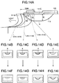
- Fig. 14A is a tracing of a photo of a cross section of an LED array specimen which was actually manufactured in a similar way to Fig. 13, Figs. 14B - 14E schematically show the configurations of the P/N junctions 4 when viewed from the front of the second surface 111d in the direction parallel to the first surface 111c, and Figs. 14F - 14I schematically show the light extracted from the second surface 111d when viewed from the front of the second surface 111d in the direction parallel to the first surface 111c.
- the configuration of the P/N junction 4 of prior art is like a narrow curved line as shown in Fig. 14E, the light intensity emitted from the P/N junction 4 of the prior art LED is small as shown in Fig. 14I.
- the configuration of the cross section of the light is semicircular but its intensity is smaller than when Lme is 1.2Xj. This is because the N-type semiconductor substrate 111 remaining between the P/N junction 4 and the second surface 111d is long, and the light intensity absorbed therein is large.
- the configuration of the cross section of the light is arc but its intensity is smaller than when Lme is 1.2Xj. This is because when the configuration of the P/N junction 4 is belt-shaped as shown in Fig. 14D and the configuration of the cross section of the light is also belt-shaped as shown in Fig. 14H, lighting area is reduced, so the light intensity is small.
- Fig. 15 is a graph showing a relation between a length Lme from an edge of the aperture 121a in the diffusion prevention film 121 to the edge formed by etching, and an end face light emitting intensity, in the end face light-emitting-type LED according to the second embodiment.
- the vertical axis shows relative light emitting intensity (arbitrary scale) and the horizontal axis shows Lme length (relation to the depth Xj of the diffusion region 113).
- the side diffusion length which is the diffusion length in a horizontal direction from the aperture 121a of the diffusion prevention film 121 to beneath the diffusion prevention film 121, as can be seen also from the fact that the slant angle ⁇ in the cross section of the side diffusion part is approximately 40° , has a length which is approximately 1.2 times the diffusion depth Xj.
- the oblique part of the P/N junction on the end face side is cut by etching so the light intensity decreases.
- the end face position is therefore set by etching such that Lme is equal to from 0.4 times to 2.4 times Xj, i.e., so that the following relational expression (1) 0.4 ⁇ Lme / Xj ⁇ 2.4 is satisfied.
- good chips are selected based on probing determination data, and connected to a drive circuit to fabricate a printer head. After the good chips have been incorporated in the head, they are coated with varnish or the like, as has been described above, so as to improve light extraction efficiency.
- the slant angle in a cross section of the side diffusion part of a P-type GaAsP region 113 approximates to the order of 40° , and the shape of the main part of a reverse-tapered contour of a depression 128 is approximately 75° .
- the difference between these angles is small, light is emitted efficiently and the emitted light can be extracted with high efficiency.
- the difference between the two angles is within approximately 50° .
- N-type semiconductor substrate 111 has the second surface 111d intersecting the first surface 111c at an angle ⁇ , and light is emitted from the P/N junction 4 between the N-type semiconductor substrate 111 and the P-type diffusion region 113 through the second surface 111d. The emitted light is extracted from the second surface in a direction parallel to the first surface.
- the first-conductive-type semiconductor is treated as N-type and the second-conductive-type semiconductor is treated as P-type.
- the first-conductive-type semiconductor is P-type and the second-conductive-type semiconductor is N-type.
- the second surface is formed with higher accuracy than that formed by dicing. Since the light emitting area is protected from lack or defects resulting from dicing, LED with small light intensity variation and high reliability can be formed.
- first and second embodiments describe the cases in which the light is extracted from the second surface in the direction parallel to the first surface.
- the direction of extracted light is perpendicular to the second surface, the light can be extracted with higher efficiency.
- ⁇ c sin -1 (n 2 /n 1 ) where ⁇ c is referred to as the critical angle. If the light impinges on the interface with an incident angle larger than the critical angle, the light is totally reflected, so no light can be extracted outside from the substrate.
- n 1 denotes the refractive index of the substrate, and the GaAsP substrate of this embodiment has the refractive index of 3.57.
- n 2 denotes the refractive index of air and is 1.0. In this case, the critical angle is 16.3° . If the incident angle of the light is equal to or more than the critical angle, the light can not be emitted from the end face.
- the direction of the extracted light is perpendicular to the second surface 11d or 111d, the light can be extracted from the end face with higher efficiency.
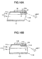
- Fig. 16A schematically shows the element of the first embodiment in which the light is extracted in a direction perpendicular to the second surface 11d
- Fig. 16B schematically shows the element of the second embodiment in which the light is extracted in a direction perpendicular to the second surface 111d.
- the end face light-emitting-type LED array should be equipped obliquely and some idea for equipment is required.
- the light intensity of the extracted light can be increased in comparison with the first and second embodiments.
- Fig. 17A schematically shows a light source device comprising the LED array of the first embodiment and a lens
- Fig. 17B schematically shows a light source device comprising the LED array of the second embodiment and a lens.
- the light is extracted from the second surface in a direction parallel to the first surface, and the optical axis AX of the lens 130 coincides with the direction of the extracted light.
- Fig. 17C schematically shows a light source device comprising the LED array of the third embodiment and a lens
- Fig. 17D schematically shows a light source device comprising the LED array of the fourth embodiment and a lens.
- the light is extracted from and perpendicular to the second surface, and the optical axis AX of the lens 130 coincides with the direction of the extracted light.
Landscapes
- Led Devices (AREA)
- Printers Or Recording Devices Using Electromagnetic And Radiation Means (AREA)
Applications Claiming Priority (4)
| Application Number | Priority Date | Filing Date | Title |
|---|---|---|---|
| JP325918/95 | 1995-12-14 | ||
| JP32591895 | 1995-12-14 | ||
| JP31587396A JP3176856B2 (ja) | 1995-12-14 | 1996-11-27 | 端面発光型led、端面発光型ledアレイ、光源装置及びそれらの製造方法 |
| JP315873/96 | 1996-11-27 |
Publications (2)
| Publication Number | Publication Date |
|---|---|
| EP0779667A2 true EP0779667A2 (de) | 1997-06-18 |
| EP0779667A3 EP0779667A3 (de) | 1999-05-19 |
Family
ID=26568456
Family Applications (1)
| Application Number | Title | Priority Date | Filing Date |
|---|---|---|---|
| EP96119979A Withdrawn EP0779667A3 (de) | 1995-12-14 | 1996-12-12 | Lichtemittierende Diode mit Kantenemission, Anordnung einer lichtemittierenden Diode mit Kantenemission und Herstellungsverfahren |
Country Status (3)
| Country | Link |
|---|---|
| US (1) | US5869848A (de) |
| EP (1) | EP0779667A3 (de) |
| JP (1) | JP3176856B2 (de) |
Cited By (3)
| Publication number | Priority date | Publication date | Assignee | Title |
|---|---|---|---|---|
| FR2765422A1 (fr) * | 1997-06-30 | 1999-01-01 | Samsung Electronics Co Ltd | Amplificateur a fibre optique muni d'un absorbeur |
| WO2001061764A1 (de) * | 2000-02-15 | 2001-08-23 | Osram Opto Semiconductors Gmbh | Strahlungsemittierendes halbleiterbauelement, verfahren zu seiner herstellung und strahlungsemittierendes optisches bauelement |
| US7205578B2 (en) | 2000-02-15 | 2007-04-17 | Osram Gmbh | Semiconductor component which emits radiation, and method for producing the same |
Families Citing this family (12)
| Publication number | Priority date | Publication date | Assignee | Title |
|---|---|---|---|---|
| DE10032838B4 (de) * | 2000-07-06 | 2015-08-20 | Osram Opto Semiconductors Gmbh | Strahlung emittierender Halbleiterchip und Verfahren zu dessen Herstellung |
| US7372663B2 (en) | 2004-03-19 | 2008-05-13 | Seagate Technology Llc | Lubricated limiter for fluid dynamic bearing motor |
| US7652299B2 (en) * | 2005-02-14 | 2010-01-26 | Showa Denko K.K. | Nitride semiconductor light-emitting device and method for fabrication thereof |
| JP4901117B2 (ja) * | 2005-03-04 | 2012-03-21 | 株式会社東芝 | 半導体発光素子及び半導体発光素子の製造方法 |
| KR101063285B1 (ko) * | 2009-06-17 | 2011-09-07 | (주)더리즈 | 방사각이 제어된 반도체 칩 |
| KR101088392B1 (ko) * | 2009-06-24 | 2011-12-01 | 주식회사 세미콘라이트 | 발광소자 칩 및 이의 제조방법 |
| CN103190004B (zh) * | 2010-09-01 | 2016-06-15 | 夏普株式会社 | 发光元件及其制造方法、发光装置的制造方法、照明装置、背光灯、显示装置以及二极管 |
| CN102270717B (zh) * | 2011-07-15 | 2013-03-06 | 华灿光电股份有限公司 | 一种弯曲衬底侧面的发光二极管芯片及其制备方法 |
| KR20150101783A (ko) * | 2014-02-27 | 2015-09-04 | 서울바이오시스 주식회사 | 발광 다이오드 및 그 제조 방법 |
| JP6569291B2 (ja) * | 2015-05-13 | 2019-09-04 | 日亜化学工業株式会社 | 発光素子 |
| JP6822429B2 (ja) | 2018-02-19 | 2021-01-27 | 日亜化学工業株式会社 | 発光素子 |
| US11282984B2 (en) * | 2018-10-05 | 2022-03-22 | Seoul Viosys Co., Ltd. | Light emitting device |
Family Cites Families (8)
| Publication number | Priority date | Publication date | Assignee | Title |
|---|---|---|---|---|
| JPS5630776A (en) * | 1979-08-21 | 1981-03-27 | Oki Electric Ind Co Ltd | Manufacture of light emitting element array |
| JPS5775473A (en) * | 1980-10-29 | 1982-05-12 | Nec Corp | Semiconductor light-emitting element |
| JPS5779482A (en) * | 1980-11-05 | 1982-05-18 | Ricoh Elemex Corp | Method for correcting time of electronic timepiece |
| JPH02125765A (ja) * | 1988-11-04 | 1990-05-14 | Mitsubishi Electric Corp | Ledアレイ・ヘッド |
| JPH04343484A (ja) * | 1991-05-21 | 1992-11-30 | Eastman Kodak Japan Kk | 発光ダイオードアレイ |
| JP3205049B2 (ja) * | 1992-06-11 | 2001-09-04 | 株式会社リコー | 光プリンター用光源 |
| JPH06283757A (ja) * | 1993-03-25 | 1994-10-07 | Kyocera Corp | Ledアレイの製造方法 |
| JPH06310755A (ja) * | 1993-04-27 | 1994-11-04 | Matsushita Electric Ind Co Ltd | Ledアレイチップおよびその製造方法 |
-
1996
- 1996-11-27 JP JP31587396A patent/JP3176856B2/ja not_active Expired - Fee Related
- 1996-12-09 US US08/762,417 patent/US5869848A/en not_active Expired - Lifetime
- 1996-12-12 EP EP96119979A patent/EP0779667A3/de not_active Withdrawn
Cited By (5)
| Publication number | Priority date | Publication date | Assignee | Title |
|---|---|---|---|---|
| FR2765422A1 (fr) * | 1997-06-30 | 1999-01-01 | Samsung Electronics Co Ltd | Amplificateur a fibre optique muni d'un absorbeur |
| WO2001061764A1 (de) * | 2000-02-15 | 2001-08-23 | Osram Opto Semiconductors Gmbh | Strahlungsemittierendes halbleiterbauelement, verfahren zu seiner herstellung und strahlungsemittierendes optisches bauelement |
| US6730939B2 (en) | 2000-02-15 | 2004-05-04 | Osram Opto Semiconductors Gmbh | Radiation emitting semiconductor device |
| US7195942B2 (en) | 2000-02-15 | 2007-03-27 | Osram Gmbh | Radiation emitting semiconductor device |
| US7205578B2 (en) | 2000-02-15 | 2007-04-17 | Osram Gmbh | Semiconductor component which emits radiation, and method for producing the same |
Also Published As
| Publication number | Publication date |
|---|---|
| EP0779667A3 (de) | 1999-05-19 |
| US5869848A (en) | 1999-02-09 |
| JPH09223818A (ja) | 1997-08-26 |
| JP3176856B2 (ja) | 2001-06-18 |
Similar Documents
| Publication | Publication Date | Title |
|---|---|---|
| EP0779667A2 (de) | Lichtemittierende Diode mit Kantenemission, Anordnung einer lichtemittierenden Diode mit Kantenemission und Herstellungsverfahren | |
| US10381516B2 (en) | Semiconductor light emitting device having a recess with irregularities | |
| JP3232152B2 (ja) | 発光ダイオードアレイ | |
| US20090227088A1 (en) | Semiconductor wafer and manufacturing process for semiconductor device | |
| US20080199983A1 (en) | Method for manufacturing a semiconductor laser | |
| US6335559B1 (en) | Semiconductor device cleave initiation | |
| US6335215B1 (en) | Self-alignment method of making | |
| EP0872898B1 (de) | Leuchtdiodenanordnung | |
| US6882672B2 (en) | Point emission type light emitting element and concentrating point emission type light emitting element | |
| EP0871226B1 (de) | Herstellungsverfahren eines Halbleiterplättchens mit lichtempfangender/lichtemittierender Diodenanordnung | |
| US20250192516A1 (en) | Laser diode component, laser diode apparatus and method for producing a laser diode component | |
| JPH09102473A (ja) | 半導体装置の製造方法 | |
| US8216868B2 (en) | Method of fabricating semiconductor laser | |
| US5866439A (en) | Method of fabricating an end face light emitting type light-emitting diode and a light-emitting diode array device | |
| JPH0945957A (ja) | 端面発光型ledアレイの製造方法及びその検査方法 | |
| JPH09191038A (ja) | 半導体デバイスの製造方法 | |
| JP7537219B2 (ja) | アレイ素子の製造方法、製造装置、および製造プログラム | |
| US20250248182A1 (en) | Light-emitting device | |
| JPH0945958A (ja) | 端面発光型ledアレイ及びその製造方法 | |
| JP4126163B2 (ja) | 半導体装置、ledチップ及びその製造方法 | |
| JPH08183199A (ja) | 端面発光型発光素子および製法、端面発光型発光素子用の配線基板、端面発光型発光素子の実装方法、光プリントヘッド | |
| JPH1012919A (ja) | 受発光素子、受発光素子アレイ、受発光素子の製造方法 | |
| JPH08222529A (ja) | ダイシングマーク、ダイシングマークの形成方法、ダイシング方法、およびダイシング検査方法 | |
| JP2026061163A (ja) | 半導体レーザ素子の製造方法 | |
| JP2005277152A (ja) | 点光源発光ダイオードおよびその製造方法 |
Legal Events
| Date | Code | Title | Description |
|---|---|---|---|
| PUAI | Public reference made under article 153(3) epc to a published international application that has entered the european phase |
Free format text: ORIGINAL CODE: 0009012 |
|
| AK | Designated contracting states |
Kind code of ref document: A2 Designated state(s): DE GB NL |
|
| PUAL | Search report despatched |
Free format text: ORIGINAL CODE: 0009013 |
|
| AK | Designated contracting states |
Kind code of ref document: A3 Designated state(s): DE GB NL |
|
| 17P | Request for examination filed |
Effective date: 19991022 |
|
| RAP1 | Party data changed (applicant data changed or rights of an application transferred) |
Owner name: OKI DATA CORPORATION |
|
| 17Q | First examination report despatched |
Effective date: 20040415 |
|
| STAA | Information on the status of an ep patent application or granted ep patent |
Free format text: STATUS: THE APPLICATION IS DEEMED TO BE WITHDRAWN |
|
| 18D | Application deemed to be withdrawn |
Effective date: 20040826 |