EP0774704A2 - Niederspannungs-Referenzschaltung und Betriebsverfahren - Google Patents
Niederspannungs-Referenzschaltung und Betriebsverfahren Download PDFInfo
- Publication number
- EP0774704A2 EP0774704A2 EP96118443A EP96118443A EP0774704A2 EP 0774704 A2 EP0774704 A2 EP 0774704A2 EP 96118443 A EP96118443 A EP 96118443A EP 96118443 A EP96118443 A EP 96118443A EP 0774704 A2 EP0774704 A2 EP 0774704A2
- Authority
- EP
- European Patent Office
- Prior art keywords
- voltage
- current
- terminal
- transistor
- coupled
- Prior art date
- Legal status (The legal status is an assumption and is not a legal conclusion. Google has not performed a legal analysis and makes no representation as to the accuracy of the status listed.)
- Withdrawn
Links
- 238000000034 method Methods 0.000 title claims description 20
- 230000001419 dependent effect Effects 0.000 claims description 5
- 238000012358 sourcing Methods 0.000 claims 2
- 239000004065 semiconductor Substances 0.000 claims 1
- 238000012546 transfer Methods 0.000 description 12
- 230000000694 effects Effects 0.000 description 7
- XUIMIQQOPSSXEZ-UHFFFAOYSA-N Silicon Chemical compound [Si] XUIMIQQOPSSXEZ-UHFFFAOYSA-N 0.000 description 6
- 229910052710 silicon Inorganic materials 0.000 description 6
- 239000010703 silicon Substances 0.000 description 6
- 239000003990 capacitor Substances 0.000 description 4
- 238000011982 device technology Methods 0.000 description 4
- 238000005516 engineering process Methods 0.000 description 4
- 238000013459 approach Methods 0.000 description 2
- 238000012545 processing Methods 0.000 description 2
- 230000002596 correlated effect Effects 0.000 description 1
- 238000013461 design Methods 0.000 description 1
- 238000010586 diagram Methods 0.000 description 1
- 238000009792 diffusion process Methods 0.000 description 1
- 238000004519 manufacturing process Methods 0.000 description 1
- 238000012986 modification Methods 0.000 description 1
- 230000004048 modification Effects 0.000 description 1
- 238000012544 monitoring process Methods 0.000 description 1
Images


Classifications
-
- G—PHYSICS
- G05—CONTROLLING; REGULATING
- G05F—SYSTEMS FOR REGULATING ELECTRIC OR MAGNETIC VARIABLES
- G05F3/00—Non-retroactive systems for regulating electric variables by using an uncontrolled element, or an uncontrolled combination of elements, such element or such combination having self-regulating properties
- G05F3/02—Regulating voltage or current
- G05F3/08—Regulating voltage or current wherein the variable is DC
- G05F3/10—Regulating voltage or current wherein the variable is DC using uncontrolled devices with non-linear characteristics
- G05F3/16—Regulating voltage or current wherein the variable is DC using uncontrolled devices with non-linear characteristics being semiconductor devices
- G05F3/20—Regulating voltage or current wherein the variable is DC using uncontrolled devices with non-linear characteristics being semiconductor devices using diode- transistor combinations
- G05F3/24—Regulating voltage or current wherein the variable is DC using uncontrolled devices with non-linear characteristics being semiconductor devices using diode- transistor combinations wherein the transistors are of the field-effect type only
- G05F3/242—Regulating voltage or current wherein the variable is DC using uncontrolled devices with non-linear characteristics being semiconductor devices using diode- transistor combinations wherein the transistors are of the field-effect type only with compensation for device parameters, e.g. channel width modulation, threshold voltage, processing, or external variations, e.g. temperature, loading, supply voltage
- G05F3/245—Regulating voltage or current wherein the variable is DC using uncontrolled devices with non-linear characteristics being semiconductor devices using diode- transistor combinations wherein the transistors are of the field-effect type only with compensation for device parameters, e.g. channel width modulation, threshold voltage, processing, or external variations, e.g. temperature, loading, supply voltage producing a voltage or current as a predetermined function of the temperature
-
- Y—GENERAL TAGGING OF NEW TECHNOLOGICAL DEVELOPMENTS; GENERAL TAGGING OF CROSS-SECTIONAL TECHNOLOGIES SPANNING OVER SEVERAL SECTIONS OF THE IPC; TECHNICAL SUBJECTS COVERED BY FORMER USPC CROSS-REFERENCE ART COLLECTIONS [XRACs] AND DIGESTS
- Y10—TECHNICAL SUBJECTS COVERED BY FORMER USPC
- Y10S—TECHNICAL SUBJECTS COVERED BY FORMER USPC CROSS-REFERENCE ART COLLECTIONS [XRACs] AND DIGESTS
- Y10S323/00—Electricity: power supply or regulation systems
- Y10S323/907—Temperature compensation of semiconductor
Definitions
- This invention relates generally to voltage references and more specifically to a low voltage bandgap voltage reference.
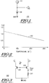
- FIG. 1 illustrates a known circuit 100 used to generate the voltage Vj 102.
- the circuit 100 has a current source 104 connected to a diode 106, such that the diode 106 is forward biased.
- the voltage Vj is the forward bias voltage of the diode 106.
- FIG. 2 illustrates graphically the known transfer characteristic curve of the voltage Vj 102 over temperature.
- the horizontal-axis of the graph represents absolute temperature in degrees Kelvin.
- the vertical-axis represents the voltage Vj 102.
- a junction formed with a typical process would have a junction voltage Vj 102 between 0.4 and 0.7 volts.
- the junction voltage would be limited by the bandgap voltage (V BG ).
- the bandgap voltage for silicon is a known, nearly constant value of approximately 1.2 volts.
- the transfer characteristic curve is represented by a nearly linear curve between the voltage value at 0°K and the voltage value at 300°K. These voltage values are approximately 1.2 volts and 0.5 volts respectively. Therefore, the transfer characteristic curve has a negative slope.
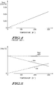
- FIG. 3 illustrates a known voltage proportional to temperature (VPT) generator circuit 300 used to generate the voltage Vpat. While a VPT generator can be generated in either MOS or bipolar technology, the illustrated VPT generator 300 depends on the exponential diffusion dominant nature of the sub-threshold current in an MOS device. As such, if the current densities in transistors 308 and 306 are sufficiently small so that the transistors operate in the sub-threshold region, also called the weak inversion region, a voltage proportional to absolute temperature will be present at node 312, providing the width of transistor 306 is greater than that of transistor 308, their lengths are substantially identical, and the gate electrode voltage applied to both transistors 306 and 308 is such that they both carry the same value of current.
- FIG. 1 voltage proportional to temperature
- Vpat voltage proportional to absolute temperature
- the horizontal-axis represents the temperature in degrees Kelvin. As the temperature approaches absolute zero (0°K), Vpat approaches zero volts.
- the transfer characteristic curve is represented by a line between a value of 20 to 80 millivolts at room temperature, depending on the ratio of the size of transistor 306 to the size of transistor 308 and the particular device process technology used for the transistors, and zero volts at absolute zero. The curve is linear and has a positive slope.
- FIG. 5 illustrates a transfer characteristic curve for a Vj labeled 504 and an amplified transfer characteristic curve for a Vpat labeled 506.
- the transfer characteristic curve for Vj 202 (FIG. 2), and the transfer characteristic curve for Vpat (FIG. 4), have slopes in opposite directions.
- Amplifying the slope of Vpat (FIG. 4) provides a slope equal to but opposite that of the slope of Vj 505.
- This amplified slope is represented by the curve 506.
- Adding the Vj voltage curve 504 and the amplified voltage curve 506 provides a voltage reference curve (Vref) 502 that is independent of temperature variation.
- the slope of Vref curve 502 is essentially zero.
- the further use of voltage shifting techniques allows the voltage reference level to be shifted to values above or below 1.2 volts.
- bandgap voltage reference generators While the use of bandgap voltage reference generators is widespread, they have been limited to use with power supply voltages above the bandgap voltage of approximately 1.2 volts. Present applications requiring batteries and lower voltages have created a need for voltage references below the 1.2 volts reference value. Therefore, the need exists for a bandgap type voltage reference generator that can operate with and generate low voltages, and for a voltage reference generator that can generate multiple reference voltages.
- the present invention provides a method and apparatus for a low supply voltage reference voltage generator.
- voltage reference generators typically require a supply voltage of greater than 1.2 volts.
- the present invention can operate with a power supply voltage at or below 0.9 volt, and generate low voltage references below 0.9 volt as well.
- FIG. 6 illustrates a voltage generator circuit 600 in accordance with the present invention.
- the voltage generator circuit 600 includes a voltage-proportional-to-absolute temperature generator 602 (VPT generator), a junction voltage reference generator 604, and a summation network 606.
- VPT generator voltage-proportional-to-absolute temperature generator 602
- the VPT generator 602 produces a voltage signal Vpat 610 which is a temperature dependent voltage reference.
- the signal Vpat 610 varies proportionally to absolute temperature, between 20 to 80 millivolts at room temperature, depending on the ratio of the size of transistor 306 to the size of transistor 308 and the particular device process technology used for the transistors, and 0.0 volts at absolute zero.
- the junction voltage reference generator 604 generates the signal Vj 608 which is a junction voltage reference.
- This signal is a representation of a bipolar junction voltage as illustrated in FIG. 2.
- the summation network 606 receives the signals Vpat 610 and a buffered junction voltage reference Vj' 612. Upon receiving these signals, the summation network 606 produces the reference voltage Vref 614.
- FIG. 7 illustrates a junction voltage reference generator 604 in accordance with the invention.
- the generator 604 comprises a current source 709, a diode 702 having a bipolar junction, and a buffer 706.
- the current source 709 is connected to the diode 702 such that diode 702 is forward biased creating a voltage reference Vj across the diode.
- the input to buffer 706 is connected to receive Vj 708, which is generated at the node common to current source 709 and diode 702.
- the buffer 706 can be implemented using a unity gain amplifier.
- the output of buffer 706 is signal Vj' 612 which is proportional to the diode voltage at the input of buffer 706.
- the buffer 706 is used to prevent loading at the output portion of the circuit from affecting the voltage Vj 708.
- the summation network 606 comprises a divide circuit 620, a multiply circuit 630, and a summation circuit 618.
- the divide circuit 620 receives signal Vj' 612 and provides a divided signal 616 as its output.
- the voltage multiply circuit 630 receives signal Vpat 610 and provides a multiplied signal 622 as its output.
- the divided signal 616 and the multiplied signal 622 are received by the summation circuit 618. These two received signals are summed together by the summation circuit 618. The summation of these signals produces a reference voltage as its output. As illustrated in FIG.
- the voltage Vref 502 which is analogous to reference voltage 614, is generated by summing together the Vj 504 and the amplified Vpat signal 506.
- the slopes of these representations are opposite such that their combination provides a temperature independent voltage as represented by signal Vref 502.
- a prior art limitation occurs because of the bandgap voltage.
- the bandgap voltage of a silicon bipolar junction is approximately 1.2 volts. To generate a voltage reference of 1.2 volts, it would require a supply voltage of somewhat more than 1.2 volts. Therefore, the lowest operating voltage, in an ideal situation, would be greater than 1.2 volts.
- the addition of the divide circuit 620 as shown in FIG. 6 allows the slope of the Vj versus temperature transfer characteristic curve (FIG. 2) to be changed. By changing the slope of this curve, the point at which the transfer characteristic curve intercepts the vertical-axis is also modified. For example, if the voltage divide circuit 620 divided the Vj' input signal, represented by the transfer characteristic curve 504 of FIG.
- the new vertical-axis intercept would be at 0.6 volt.
- the vertical-intercept of 0.6 volt now represents the voltage reference that can be generated. This is accomplished by amplifying Vpat 610 so that its slope is approximately the inverse of the slope of the curve representative of Vj' 612. Now that the reference voltage is 0.6 volt, it is possible to operate at a supply voltage of 0.9 volt or less.
- the 0.9 volt is representative of a minimum supply voltage available in many battery operated applications.
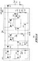
- FIG. 8 illustrates a low voltage reference circuit 800 in accordance with the present invention.
- the voltage reference circuit 800 implements the VPT generator 602 with P-channel transistors 802, and 806, N-channel transistors 804, and 808, and resistor 810.
- This implementation of the voltage-proportional-to-absolute-temperature generator 602 is known prior art.
- Transistor 802 has a source electrode connected to a power supply V DD , a drain electrode, and a gate electrode.
- Transistor 806 has a source electrode connected to power supply V DD , a drain electrode, and a gate electrode connected to the drain electrode of transistor 806 and to the gate electrode of transistor 802.
- Transistor 804 has a drain electrode connected to the drain electrode of transistor 802, a source electrode connected to receive a ground signal, and a gate electrode connected to the drain electrode of transistor 804.
- Transistor 808 has a drain electrode connected to the drain electrode of transistor 806, a source electrode connected to a first terminal of a resistor 810, and a gate electrode connected to the gate electrode of transistor 804.
- the resistor 810 has a second terminal connected to the ground signal.
- the node common to the source electrode of transistor 808 and the first terminal of resistor 810 is node 836.
- the node 836 is analogous to the signal Vpat 610 of FIG. 6.
- the current density in N-channel transistor 804 and N-channel transistor 808 of the VPT generator 602 is sufficiently low so that these transistors operate in the sub-threshold or weak inversion region, and in accordance with one embodiment of the invention, the transistor width ratio is such that the width of transistor 808 is four times that of transistor 804.
- the VPT generator 602 as shown in FIG. 8 will produce a voltage reference at node 836 of 35 to 50 millivolts depending on the characteristics of the particular silicon device technology used for the circuit.
- the node 836 is analogous to the signal Vpat 610 of FIG. 6.
- the amount of current passing through transistor 806 and transistor 808 is controlled by the resistor 810.
- the resistor 810 would be chosen to be 40 kilo-ohms. This current is proportional to the voltage Vpat.
- Transistors 806 and 802 form a current mirror. If transistors 802 and 806 are substantially the same, the current in transistor 802 will be the same as the current in transistor 806, if the effects of output impedance and process variation are disregarded. Transistor 802 controls the current in transistor 804 thus assuring that transistors 804 and 808 carry the same current if the effects of output impedance and process variation are disregarded.
- the current can be replicated in other parts of the circuit by driving the gate electrode of an N-channel or a P-channel transistor with the gate electrode voltage of N-channel transistor 804 or P-channel transistor 806 respectively.
- the junction voltage generator 604 (FIG. 6) is implemented as illustrated in FIG. 8 using a P-channel transistor 812, a diode 814, and an amplifier 850.
- N-channel transistor 850 and P-channel transistor 848 control the current in P-channel transistor 812.
- the amplifier 850 comprises P-channel transistors 816, 822, and 826, N-channel transistors 818, 824, and 820, and resistors 828 and 830.
- P-channel transistor 844 and N-channel transistor 846 set up the current bias for the amplifier.
- Transistor 850 has a gate electrode connected to the gate electrode of transistor 804, a source electrode connected to receive the ground signal, and a drain electrode.
- Transistor 848 has a source electrode connected to power supply V DD , a drain electrode connected to the drain electrode of transistor 850, and a gate electrode connected to the drain electrode of transistor 848.
- Transistor 812 has a gate electrode connected to the gate electrode of transistor 848, a source electrode connected to power supply V DD , and a drain electrode.
- the diode 814 has an anode connected to the drain electrode of transistor 812, and a cathode connected to the ground signal.
- the node common to the diode 814 and transistor 812 is node 838, which represents the forward biased junction voltage of the diode Vj 608 of FIG. 6.
- Transistor 816 has a source electrode connected to power supply V DD , a gate electrode, and a drain electrode.
- Transistor 818 has a drain electrode connected to the drain electrode of transistor 816, a gate electrode connected to node 838, and a source electrode.
- Transistor 844 has a gate source electrode connected to power supply V DD , a gate electrode connected to the gate electrode of transistor 806, and a drain electrode.
- Transistor 846 has a source electrode connected to the ground signal, a drain electrode connected to the drain electrode of transistor 844, and a gate electrode connected to the drain electrode of transistor 846.
- Transistor 820 has a drain electrode connected to the source electrode of transistor 818, a gate electrode connected to the gate electrode of transistor 846, and a source electrode connected to the ground signal.
- the transistor 822 has a source electrode connected to power supply V DD , a gate electrode connected to the gate electrode of transistor 816, and a drain electrode connected to the gate electrode of transistor 822.
- the transistor 824 has a drain electrode connected to the drain electrode of transistor 822, a gate electrode, and a source electrode connected to the drain electrode of transistor 820.
- the transistor 826 has a source electrode connected to power supply V DD , a gate electrode connected to the drain electrode of transistor 818 and the first terminal of capacitor 860, and a drain electrode connected to the gate electrode of transistor 824 and the second terminal of capacitor 860, and to a first terminal of a resistor 828.
- the resistor 828 has a second terminal connected to a first terminal of a resistor 830.
- the resistor 830 has a second terminal connected to the ground signal.
- Node 852 is the node common to the second terminal of resistor 828 and to the first terminal of resistor 830.
- Node 840 is the node common to the drain electrode of transistor 826, the gate electrode of transistor 824 and the first terminal of resistor 828.
- the node 840 is analogous to signal Vj' 612 of FIG. 6.
- the N-channel transistor 850 acts as a current source and receives the same gate electrode voltage that drives the gate of transistor 804. Typically, transistor 850 has a much smaller width than transistor 804 and conducts a much smaller current.
- the P-channel transistors 848 and 812 acts as a current mirror. The current generated by P-channel transistor 812 passes through diode 814, creating a forward junction bias across diode 814.
- a junction voltage (Vj 608 of FIG. 6) is present at a node 838. The junction voltage is buffered through the amplifier 850. Vj is received by the amplifier 850 input that is the gate electrode of N-channel transistor 818. The output of the amplifier is at an output node 840.
- the voltage present at output node 840, Vj' 612 of FIG. 6, is substantially similar to the diode voltage present at node 838, Vj 608 of FIG. 6.
- the summation network 606 (FIG. 6) is represented in FIG. 8 by P-channel transistors 806 and 832, N-channel transistor 808, and resistors 810, 834, 828, and 830. (P-channel transistor 806, N-channel transistor 808, and resistor 810 are also part of VPT generator 602. Resistors 828 and 830 are also part of amplifier 850.)
- the divide circuit 620 (FIG. 6) is represented by the series connection of resistor 828 and resistor 830. Resistor 828 is connected to node 840 which provides a signal analogous to signal Vj' 612 (FIG. 6).
- the multiply circuit 630 (FIG. 6) is represented by the transistors 806, 808, 832 and resistors 810, 828, 830 and 834.
- the summation circuit 618 (FIG. 6) is represented by resistors 828, 830, and 834.
- Transistor 832 has a source electrode connected to the power supply V DD , a gate electrode connected to the gate electrode of transistor 806, and a drain electrode connected to a first terminal of a resistor 834.
- the second terminal of the resistor 834 is connected to node 852.
- a node common to the drain electrode of transistor 832 and to the first terminal of resistor 834 is node 614 which represents the reference voltage Vref 614 (FIG. 6).
- the voltage Vj' 612 which is represented at node 840 is coupled to a resistor divider network consisting of resistor 828 in series with resistor 830.
- Node 852 is the node common to the two resistors 828 and 830.
- resistors 828 and 830 act as a divide circuit, and node 852 is analogous to the node at which the divided signal 616 is present in FIG. 6, the signal present at node 852 is not equivalent to the divided signal 616 of FIG. 6 because the resistors 828 and 830 are also part of the summation circuit 618 of FIG. 6 which modifies the result of the resistor divider network.
- Resistors 828, 830, and 834 form a linear network with, what is effectively two sources, a voltage source, Vj', at node 840 and a current source, transistor 832. If the superposition principle is used, then from the point of view of the voltage source, Vj', the network looks like resistor 828 is in series with resistor 830 between the voltage source Vj' and the ground signal with resistor 834 connected at node 852 and being unconnected at its other terminal. From this point of view, node 852 is equivalent to node 616 of FIG. 6.
- resistor 810 connecting node 836 which represents signal Vpat 610 of FIG. 6, and the ground signal causes a current proportional to the voltage Vpat to flow through resistor 810 and transistors 808 and 806.
- Transistors 806 and 832 form a current mirror. If transistors 806 and 832 are substantially the same except for the width of the transistors then the current in transistor 832 will be a multiple of the current in transistor 806 with the multiplier being the ratio of the width of transistor 832 to the width of transistor 806 if the effects of output impedance and process variation are disregarded.
- the current from transistor 832 flows into resistor 834 and resistors 828 and 830.
- the network looks like resistor 834 is in series with the parallel combination of resistor 828 and 830.
- the voltage generated across the resistor network of resistor 834 in series with the parallel combination of resistors 820 and 830 by the current from transistor 832 is a multiple of the voltage Vpat. From this superposition point of view, node 614 is equivalent to node 622 of FIG. 6.
- the multiply factor is the ratio of the width of transistor 832 to the width of transistor 806 multiplied by the ratio of resistor 810 to the combination of resistor 834 in series with the parallel combination of resistors 828 and 830.
- Resistors 828, 830, and 832 also act to sum the divided voltage from node 840 and the multiplied voltage from node 836 at node 614.
- the operation of the summation network components in FIG. 8, and specifically the generation of Vref, can be understood through the following equations:
- Vref (V40 ⁇ R30 / (R28 + R30) ) + (I32 ⁇ (R34 + (R28 ⁇ R30 / (R28 + R30) ) ) );
- V40 is equal to Vj'.
- transistors 806 and 832 are identical, except for their width, and applying the voltage present on the gate electrode of transistor 806 to the gate electrode of transistor 832, the current passing through transistor 832 will be ratioed to the current passing through transistor 806 by the ratio of the width of transistor 832 to the width of transistor 806.
- the current in transistor 806 is equal to the current through resistor 810 of the VPT generator 602. It should be noted that the words “equal,” “identical,” and “ratio" are meant to disregard the effects of output impedance and process variations.
- Vref (V40 ⁇ R30 / (R28 + R30) ) + ( V36 ⁇ (W34/W06) ⁇ (R34 + (R28 ⁇ R30 / (R28 + R30) ) ) / R10);
- Vj is multiplied by the ratio of R30 to the sum of R28 plus R30, the ratio being less than one
- Vpat is multiplied by the ratio of W34 to W06 and by the ratio of R34 in series with the parallel combination of R28 and R30 to R10, and that the divided Vj and the multiplied Vpat are added.
- resistors 828 and 830 form a first ratio
- resistors 834 and 810 form a second ratio
- resistors 828 and 810 form a third ratio
- transistor widths W34 and W06 form a fourth ratio.
- Vref (Vj ⁇ Rr1) + (Vpat ⁇ Rw4 ⁇ (Rr2 + (Rr3 ⁇ Rr1) ) );
- R10, Rr1, Rr2, Rr3, and Rw4 can provide a value of Vref below 0.9 volt and allow circuit operation at or below 0.9 volt.
- FIG. 9 illustrates another circuit embodiment in accordance with the present invention.
- the voltage reference circuit 1000 implements the VPT generator 602 with P-channel transistors 1002, and 1006, N-channel transistors 1004, and 1008, and resistor 1010.
- Transistor 1002 has a source electrode connected to a power supply V DD , a drain electrode, and a gate electrode connected to the gate electrode of transistor 1002.
- Transistor 1006 having a source electrode connected to a power supply V DD , a drain electrode, and a gate electrode connected to the drain electrode of transistor 1006 and to the gate electrode of transistor 1002.
- Transistor 1004 has a drain electrode connected to the drain electrode of transistor 1002, a source electrode connected to receive a ground signal, and a gate electrode connected to the drain electrode of transistor 1004.
- Transistor 1008 has a drain electrode connected to the drain electrode of transistor 1006, a source electrode coupled to a first terminal of a resistor 1010, and a gate electrode coupled to the gate electrode of transistor 1004.
- the resistor 1010 has a second terminal connected to receive the ground signal.
- the node common to the source electrode of transistor 1008 and the first terminal of resistor 1010 is node 1036.
- the node 1036 is analogous to the signal Vpat 610 of FIG. 6.
- the current density in N-channel transistor 1004 and N-channel transistor 1008, of the VPT generator 602, is sufficiently small so that these transistors operate in the sub-threshold or weak inversion region, and in accordance with one embodiment of the invention, the transistor width ratio is such that the width of transistor 1008 is four times that of transistor 1004.
- the VPT generator 1002 as shown in FIG. 9 will produce a voltage reference at node 1036 of 35 to 50 millivolts depending on the characteristics of the particular silicon device technology used for the circuit.
- the amount of current passing through transistor 1006 and transistor 1008 is controlled by the resistor 1010.
- Transistor 1006 and 1002 form a current mirror. If transistors 1002 and 1006 are substantially the same then the current in transistor 1002 will be the same as the current in transistor 1006 if the effects of output impedance and process variation are disregarded. Transistor 1002 controls the current in transistor 1004 thus assuring that transistors 1004 and 1008 carry the same current if the effects of output impedance and process variation are disregarded. In addition, the current can be replicated in other parts of the circuit by driving an N-channel or a P-channel transistor with the gate electrode voltage of N-channel transistor 1008 or P-channel transistor 1006.
- the junction voltage generator 604 (FIG. 6) is implemented as illustrated in FIG. 9 using a P-channel transistor 1012, a diode 1014, and an amplifier 1050.
- N-channel transistor 1050 and P-channel transistor 1048 control the current in P-channel transistor 812.
- the amplifier 1050 comprises P-channel transistors 1016, 1022, and 1026, and N-channel transistors 1018, 1024, 1020, and 1026.
- P-channel transistor 1044 and N-channel transistor 1046 set up the current bias for the amplifier.
- Transistor 1050 has a gate electrode connected to the gate electrode of transistor 1004, a source electrode connected to receive the ground signal, and a drain electrode.
- Transistor 1048 has a source electrode connected to power supply V DD , a drain electrode connected to the drain electrode of transistor 1050, and a gate electrode connected to the drain electrode of transistor 1048.
- Transistor 1012 has a gate electrode connected to the gate electrode of transistor 1048, a source electrode connected to power supply V DD , and a drain electrode.
- the diode 1014 has an anode connected to the drain electrode of transistor 1012, and a cathode connected to receive the ground signal.
- the node common to the diode 1014 and the transistor 1012 is node 1038 which represents the forward biased junction voltage of the diode, Vj 608 of FIG. 6.
- Transistor 1016 has a source electrode connected to power supply V DD , a gate electrode, and a drain electrode.
- Transistor 1018 has a drain electrode connected to the drain electrode of transistor 1016, a gate electrode connected to node 1038, and a source electrode.
- Transistor 1044 has a source electrode connected to power supply V DD , a gate electrode connected to the gate electrode of transistor 1006, and a drain electrode.
- Transistor 1046 has a source electrode connected to receive the ground signal, a drain electrode connected to the drain electrode of transistor 1044, and a gate electrode connected to the drain electrode of transistor 1046.
- Transistor 1020 has a drain electrode connected to the source electrode of transistor 1018, a gate electrode connected to the gate electrode of transistor 1046, and a source electrode connected to receive the ground signal.
- the transistor 1022 has a source electrode connected to power supply V DD , a gate electrode connected to the gate electrode of transistor 1016, and a drain electrode connected to the gate electrode of transistor 1022.
- the transistor 1024 has a drain electrode connected to the drain electrode of transistor 1022, a gate electrode, and a source electrode connected to the drain electrode of transistor 1020.
- the transistor 1028 has a source electrode connected to power supply V DD , a gate electrode connected to the drain electrode of transistor 1018 and the first terminal of capacitor 1060, and a drain electrode connected to the gate electrode of transistor 1024 and the second terminal of capacitor 1060.
- Transistor 1026 has a source electrode connected to receive the ground signal, a gate electrode connected to the gate electrode of transistor 1046, and a drain electrode connected to the drain electrode of transistor 1028.
- Node 1040 is common to the drain electrode of transistor 1028, the gate electrode of transistor 1024, and the drain electrode of transistor 1026, and is the amplifier output node.
- the node 1040 is analogous to signal Vj' 612 of FIG. 6.
- the N-channel transistor 1050 acts as a current source and receives the same gate electrode voltage that drives the gate of transistor 1004. Typically, transistor 1050 has a much smaller width than transistor 1004 and conducts a much smaller current.
- the P-channel transistors 1048 and 1012 act as a current mirror. The current generated by P-channel transistor 1012 passes through diode 1014, creating a forward junction bias across diode 1014.
- the junction voltage (Vj 608 of FIG. 6) is present at a node 1038.
- the junction voltage is buffered through the amplifier 1050.
- Vj is received by the amplifier 1050 input that is the gate electrode of N-channel transistor 1018.
- the output of the amplifier is at an output node 1040.
- the voltage present at output node 1040, Vj' 612 of FIG. 6, is substantially similar to the diode voltage present at node 1038, Vj 608 of FIG. 6.
- the summation network 606 (FIG. 6) is represented in FIG. 9 by the generation of a current proportional to Vpat in the voltage-proportional-to-absolute-temperature generator 602 by resistor 1010, P-channel transistors 1044, 1028 and 1032, N-channel transistors 1046 and 1026, and resistors 1030, and 1034.
- P-channel transistor 1028 and N-channel transistor 1026 are also part of amplifier 1050.
- Resistor 1030 has a first terminal connected to the amplifier output node 1040 and a second terminal connected to receive the ground signal.
- Transistor 1032 has a source electrode connected to power supply V DD , a gate electrode connected to the gate electrode of transistor 1028, and a drain electrode connected to the first terminal of a resistor 1034.
- Resistor 1034 has a second terminal connected to receive the ground signal.
- the node common to the drain electrode of transistor 1032 and the first terminal of resistor 1034 is Vref 614 of FIG. 6.
- the multiply circuit, the divide circuit and the summation circuit are intertwined in this embodiment of the present invention.
- Currents proportional to Vpat and Vj' are first generated by resistors 1010 and 1030 respectively.
- the current proportional to Vpat generated by resistor 1010 is mirrored by transistors 1006 and 1044, mirrored and multiplied by transistors 1046 and 1026 and then added to the current proportional to Vj' generated by resistor 1030 at node 1040.
- the current is fed through resistor 1034 to generate the reference voltage, Vref.
- the multiply circuit 630 (FIG. 6) is implemented in FIG. 9 by the generation of a current proportional to Vpat by resistor 1010 in the voltage-proportional-to-absolute-temperature generator 602, the mirroring of that current in transistors 1006 and 1044, the mirroring and multiplying of the current in transistors 1046 and 1026, the mirroring and multiplying of the current again in transistors 1028 and 1032, and the feeding of the mirrored current into resistor 1034.
- the divide circuit 620 (FIG. 6) is implemented by the generation of a current proportional to Vj by resistor 1030, the mirroring and multiplying of the current in transistors 1028 and 1032, and the feeding of the mirrored current into resistor 1034.
- 142 is divided into two current components. One component is dependent on the voltage Vj and resistor R30. The other component is dependent on Vpat, resistor R10, and the ratio of W26 to W46.
- Vref (Vj ⁇ (R34 / R30) ⁇ (W32/W28) ) + (Vpat ⁇ (R34 / R10) ⁇ (W26/W46) ⁇ (W32/W28));
- Vj is multiplied by the ratio of R34 to R30 and W32 to W28 which has a net value of less than one
- Vpat is multiplied by the ratio of R34 to R10, W26 to W46, and W32 to W28 which has a net value of greater than one
- the divided Vj and multiplied Vpat are summed.
- resistors R34 and R30 form a first ratio
- resistors R34 and R10 form a second ratio
- transistor widths W26 and W46 form a third ratio
- transistor width W32 and W28 form a fourth ratio.
- Vref (Rr1 ⁇ Rw4 ⁇ Vj) + (Rr2 ⁇ Rw3 ⁇ Rw4 ⁇ Vpat);
- R10, Rr1, Rr2, Rw3, and Rw4 can provide a value of Vref below 0.9 volt and allow circuit operation at or below 0.9 volt.
- the circuit of FIG. 9 also allows multiple reference voltages to be obtained by duplicating the structure and connections of transistor 1032 and resistor 1034. For each stage cascaded in a manner such as this, a different voltage reference can be obtained.
- the current mirror configuration allows similar or different resistors or transistor widths to be selected in order to obtain desired voltage references.
- FIG. 9 further illustrates the use of additional output stages to provide additional reference voltages.
- a P-channel transistor 1032', and a resistor 1034' can be connected in a manner similar to transistor 1032 and resistor 1034, with the gate electrode of transistor 1032' being connected to the gate electrode of transistor 1028. If transistors 1032 and 1032' are identical, then a different reference voltage may be obtained by varying the resistance value of resistor 1034'. If transistors 1032 and 1032' are identical except for the ratio of their widths, then both the transistor width ratio and the resistance value of resistor 1034' can be used to obtain the desired reference voltage. Theoretically, any number of additional output stages can be added.
- the circuit could be manufactured in MOS, Bipolar, BiCMOS, or other technologies.
- the conductivity type of the illustrated transistors may be reversed.
- junction voltage reference generator 604 that may be used, as well as other implementations of the voltage proportional to temperature generator 602. While the embodiment disclosed may specify specific transistor ratios or sizes, it is recognized that other transistor ratios and sizes could be used to meet the objectives of the invention. If desired, the invention could also be used to obtain an output voltage that varies over temperature by a known amount.
Landscapes
- Engineering & Computer Science (AREA)
- Microelectronics & Electronic Packaging (AREA)
- Physics & Mathematics (AREA)
- Nonlinear Science (AREA)
- Electromagnetism (AREA)
- General Physics & Mathematics (AREA)
- Radar, Positioning & Navigation (AREA)
- Automation & Control Theory (AREA)
- Control Of Electrical Variables (AREA)
- Amplifiers (AREA)
Applications Claiming Priority (2)
| Application Number | Priority Date | Filing Date | Title |
|---|---|---|---|
| US560876 | 1995-11-20 | ||
| US08/560,876 US5614816A (en) | 1995-11-20 | 1995-11-20 | Low voltage reference circuit and method of operation |
Publications (2)
| Publication Number | Publication Date |
|---|---|
| EP0774704A2 true EP0774704A2 (de) | 1997-05-21 |
| EP0774704A3 EP0774704A3 (de) | 1998-01-21 |
Family
ID=24239728
Family Applications (1)
| Application Number | Title | Priority Date | Filing Date |
|---|---|---|---|
| EP96118443A Withdrawn EP0774704A3 (de) | 1995-11-20 | 1996-11-18 | Niederspannungs-Referenzschaltung und Betriebsverfahren |
Country Status (4)
| Country | Link |
|---|---|
| US (1) | US5614816A (de) |
| EP (1) | EP0774704A3 (de) |
| JP (1) | JPH09160663A (de) |
| TW (1) | TW334634B (de) |
Families Citing this family (28)
| Publication number | Priority date | Publication date | Assignee | Title |
|---|---|---|---|---|
| JP3780030B2 (ja) * | 1995-06-12 | 2006-05-31 | 株式会社ルネサステクノロジ | 発振回路およびdram |
| US5629612A (en) * | 1996-03-12 | 1997-05-13 | Maxim Integrated Products, Inc. | Methods and apparatus for improving temperature drift of references |
| US5933045A (en) * | 1997-02-10 | 1999-08-03 | Analog Devices, Inc. | Ratio correction circuit and method for comparison of proportional to absolute temperature signals to bandgap-based signals |
| US5900773A (en) * | 1997-04-22 | 1999-05-04 | Microchip Technology Incorporated | Precision bandgap reference circuit |
| US6091287A (en) * | 1998-01-23 | 2000-07-18 | Motorola, Inc. | Voltage regulator with automatic accelerated aging circuit |
| US6002243A (en) * | 1998-09-02 | 1999-12-14 | Texas Instruments Incorporated | MOS circuit stabilization of bipolar current mirror collector voltages |
| US6225856B1 (en) * | 1999-07-30 | 2001-05-01 | Agere Systems Cuardian Corp. | Low power bandgap circuit |
| EP1178383B1 (de) * | 2000-08-03 | 2012-10-03 | STMicroelectronics Srl | Schaltung zur Erzeugung einer temperaturunabhängigen und wenig prozessvariableabhängigen Spannung |
| US6469572B1 (en) * | 2001-03-28 | 2002-10-22 | Intel Corporation | Forward body bias generation circuits based on diode clamps |
| KR100493174B1 (ko) * | 2003-06-16 | 2005-06-02 | 삼성전자주식회사 | 주파수 분주기용 기준 전압 발생기 및 그 방법 |
| WO2005006102A1 (en) * | 2003-07-09 | 2005-01-20 | Anton Pletersek | Temperature independent low reference voltage source |
| US7543253B2 (en) * | 2003-10-07 | 2009-06-02 | Analog Devices, Inc. | Method and apparatus for compensating for temperature drift in semiconductor processes and circuitry |
| JP2005332364A (ja) * | 2004-04-22 | 2005-12-02 | Oki Electric Ind Co Ltd | 定電流発生回路 |
| KR100582742B1 (ko) * | 2004-12-21 | 2006-05-22 | 인티그런트 테크놀로지즈(주) | 기준 전류 발생 회로 |
| JP2006244228A (ja) * | 2005-03-04 | 2006-09-14 | Elpida Memory Inc | 電源回路 |
| US7511567B2 (en) * | 2005-10-06 | 2009-03-31 | Avago Technologies Ecbu Ip (Singapore) Pte. Ltd. | Bandgap reference voltage circuit |
| JP4817825B2 (ja) * | 2005-12-08 | 2011-11-16 | エルピーダメモリ株式会社 | 基準電圧発生回路 |
| JP2007228399A (ja) * | 2006-02-24 | 2007-09-06 | Toshiba Corp | 電圧制御電流源および可変利得増幅器 |
| TWI378227B (en) * | 2009-02-27 | 2012-12-01 | Mstar Semiconductor Inc | Ptat sensor and temperature sensing method thereof |
| JP2012084034A (ja) * | 2010-10-14 | 2012-04-26 | Toshiba Corp | 定電圧定電流発生回路 |
| JP5220826B2 (ja) * | 2010-11-05 | 2013-06-26 | 株式会社半導体理工学研究センター | 基準電圧源回路 |
| US9958895B2 (en) * | 2011-01-11 | 2018-05-01 | Taiwan Semiconductor Manufacturing Company, Ltd. | Bandgap reference apparatus and methods |
| US8278995B1 (en) | 2011-01-12 | 2012-10-02 | National Semiconductor Corporation | Bandgap in CMOS DGO process |
| JP2012216034A (ja) * | 2011-03-31 | 2012-11-08 | Toshiba Corp | 定電流源回路 |
| US8924765B2 (en) * | 2011-07-03 | 2014-12-30 | Ambiq Micro, Inc. | Method and apparatus for low jitter distributed clock calibration |
| US8547166B2 (en) * | 2011-07-29 | 2013-10-01 | Macronix International Co., Ltd. | Temperature compensation circuit and temperature compensated metal oxide semiconductor transistor using the same |
| US9634648B1 (en) * | 2013-12-05 | 2017-04-25 | Xilinx, Inc. | Trimming a temperature dependent voltage reference |
| KR20230112326A (ko) * | 2022-01-20 | 2023-07-27 | 에스케이하이닉스 주식회사 | 온도 변화에도 기준 전류 혹은 기준 전압을 생성하는 반도체 장치 |
Family Cites Families (15)
| Publication number | Priority date | Publication date | Assignee | Title |
|---|---|---|---|---|
| US3617859A (en) * | 1970-03-23 | 1971-11-02 | Nat Semiconductor Corp | Electrical regulator apparatus including a zero temperature coefficient voltage reference circuit |
| US4313082A (en) * | 1980-06-30 | 1982-01-26 | Motorola, Inc. | Positive temperature coefficient current source and applications |
| US4375595A (en) * | 1981-02-03 | 1983-03-01 | Motorola, Inc. | Switched capacitor temperature independent bandgap reference |
| US4368420A (en) * | 1981-04-14 | 1983-01-11 | Fairchild Camera And Instrument Corp. | Supply voltage sense amplifier |
| US4935690A (en) * | 1988-10-31 | 1990-06-19 | Teledyne Industries, Inc. | CMOS compatible bandgap voltage reference |
| US4849684A (en) * | 1988-11-07 | 1989-07-18 | American Telephone And Telegraph Company, At&T Bell Laaboratories | CMOS bandgap voltage reference apparatus and method |
| US4945260A (en) * | 1989-04-17 | 1990-07-31 | Advanced Micro Devices, Inc. | Temperature and supply compensated ECL bandgap reference voltage generator |
| US4896094A (en) * | 1989-06-30 | 1990-01-23 | Motorola, Inc. | Bandgap reference circuit with improved output reference voltage |
| US5053640A (en) * | 1989-10-25 | 1991-10-01 | Silicon General, Inc. | Bandgap voltage reference circuit |
| US5144223A (en) * | 1991-03-12 | 1992-09-01 | Mosaid, Inc. | Bandgap voltage generator |
| US5148099A (en) * | 1991-04-01 | 1992-09-15 | Motorola, Inc. | Radiation hardened bandgap reference voltage generator and method |
| US5245273A (en) * | 1991-10-30 | 1993-09-14 | Motorola, Inc. | Bandgap voltage reference circuit |
| US5336986A (en) * | 1992-02-07 | 1994-08-09 | Crosspoint Solutions, Inc. | Voltage regulator for field programmable gate arrays |
| US5325045A (en) * | 1993-02-17 | 1994-06-28 | Exar Corporation | Low voltage CMOS bandgap with new trimming and curvature correction methods |
| EP0658835B1 (de) * | 1993-12-17 | 1999-10-06 | STMicroelectronics S.r.l. | Bandlückenspannungsreferenz mit niedriger Versorgungsspannung |
-
1995
- 1995-11-20 US US08/560,876 patent/US5614816A/en not_active Expired - Lifetime
-
1996
- 1996-10-30 TW TW085113276A patent/TW334634B/zh not_active IP Right Cessation
- 1996-11-18 EP EP96118443A patent/EP0774704A3/de not_active Withdrawn
- 1996-11-19 JP JP8323580A patent/JPH09160663A/ja active Pending
Non-Patent Citations (1)
| Title |
|---|
| None |
Also Published As
| Publication number | Publication date |
|---|---|
| TW334634B (en) | 1998-06-21 |
| US5614816A (en) | 1997-03-25 |
| EP0774704A3 (de) | 1998-01-21 |
| JPH09160663A (ja) | 1997-06-20 |
Similar Documents
| Publication | Publication Date | Title |
|---|---|---|
| US5614816A (en) | Low voltage reference circuit and method of operation | |
| US4839535A (en) | MOS bandgap voltage reference circuit | |
| KR0153545B1 (ko) | 기준 전위 발생 회로 | |
| US5774013A (en) | Dual source for constant and PTAT current | |
| DE19804747B4 (de) | Bandabstandsbezugsschaltung und Verfahren | |
| US5315230A (en) | Temperature compensated voltage reference for low and wide voltage ranges | |
| US6815941B2 (en) | Bandgap reference circuit | |
| EP0778509B1 (de) | Temperaturkompensierter Referenzstromgenerator mit Widerständen mit grossen Temperaturkoeffizienten | |
| KR0169316B1 (ko) | 기준 발생기 | |
| EP0252320B1 (de) | Referenzspannung für Transistorkonstantstromquelle | |
| US5949278A (en) | Reference current generator in CMOS technology | |
| US4059793A (en) | Semiconductor circuits for generating reference potentials with predictable temperature coefficients | |
| US7170336B2 (en) | Low voltage bandgap reference (BGR) circuit | |
| US5103159A (en) | Current source with low temperature coefficient | |
| US4088941A (en) | Voltage reference circuits | |
| US6373330B1 (en) | Bandgap circuit | |
| US4380706A (en) | Voltage reference circuit | |
| US6614209B1 (en) | Multi stage circuits for providing a bandgap voltage reference less dependent on or independent of a resistor ratio | |
| US6388507B1 (en) | Voltage to current converter with variation-free MOS resistor | |
| JP2001510609A (ja) | 温度補償された出力基準電圧を有する基準電圧源 | |
| JPS5925243B2 (ja) | 定電流源 | |
| US7675353B1 (en) | Constant current and voltage generator | |
| EP0121793A1 (de) | CMOS-Kreis mit parameterangepasstem Spannungsregler | |
| US6819093B1 (en) | Generating multiple currents from one reference resistor | |
| US7218167B2 (en) | Electric reference voltage generating device of improved accuracy and corresponding electronic integrated circuit |
Legal Events
| Date | Code | Title | Description |
|---|---|---|---|
| PUAI | Public reference made under article 153(3) epc to a published international application that has entered the european phase |
Free format text: ORIGINAL CODE: 0009012 |
|
| AK | Designated contracting states |
Kind code of ref document: A2 Designated state(s): DE GB |
|
| PUAL | Search report despatched |
Free format text: ORIGINAL CODE: 0009013 |
|
| AK | Designated contracting states |
Kind code of ref document: A3 Designated state(s): DE GB |
|
| 17P | Request for examination filed |
Effective date: 19980721 |
|
| 17Q | First examination report despatched |
Effective date: 19991229 |
|
| STAA | Information on the status of an ep patent application or granted ep patent |
Free format text: STATUS: THE APPLICATION IS DEEMED TO BE WITHDRAWN |
|
| 18D | Application deemed to be withdrawn |
Effective date: 20010807 |