EP0771027A1 - Semiconductor device - Google Patents
Semiconductor device Download PDFInfo
- Publication number
- EP0771027A1 EP0771027A1 EP96913744A EP96913744A EP0771027A1 EP 0771027 A1 EP0771027 A1 EP 0771027A1 EP 96913744 A EP96913744 A EP 96913744A EP 96913744 A EP96913744 A EP 96913744A EP 0771027 A1 EP0771027 A1 EP 0771027A1
- Authority
- EP
- European Patent Office
- Prior art keywords
- island
- wires
- semiconductor device
- cut
- semiconductor element
- Prior art date
- Legal status (The legal status is an assumption and is not a legal conclusion. Google has not performed a legal analysis and makes no representation as to the accuracy of the status listed.)
- Granted
Links
Images


Classifications
-
- H—ELECTRICITY
- H10—SEMICONDUCTOR DEVICES; ELECTRIC SOLID-STATE DEVICES NOT OTHERWISE PROVIDED FOR
- H10W—GENERIC PACKAGES, INTERCONNECTIONS, CONNECTORS OR OTHER CONSTRUCTIONAL DETAILS OF DEVICES COVERED BY CLASS H10
- H10W72/00—Interconnections or connectors in packages
-
- H—ELECTRICITY
- H10—SEMICONDUCTOR DEVICES; ELECTRIC SOLID-STATE DEVICES NOT OTHERWISE PROVIDED FOR
- H10W—GENERIC PACKAGES, INTERCONNECTIONS, CONNECTORS OR OTHER CONSTRUCTIONAL DETAILS OF DEVICES COVERED BY CLASS H10
- H10W70/00—Package substrates; Interposers; Redistribution layers [RDL]
- H10W70/40—Leadframes
- H10W70/411—Chip-supporting parts, e.g. die pads
-
- H—ELECTRICITY
- H10—SEMICONDUCTOR DEVICES; ELECTRIC SOLID-STATE DEVICES NOT OTHERWISE PROVIDED FOR
- H10W—GENERIC PACKAGES, INTERCONNECTIONS, CONNECTORS OR OTHER CONSTRUCTIONAL DETAILS OF DEVICES COVERED BY CLASS H10
- H10W70/00—Package substrates; Interposers; Redistribution layers [RDL]
- H10W70/40—Leadframes
- H10W70/481—Leadframes for devices being provided for in groups H10D8/00 - H10D48/00
-
- H—ELECTRICITY
- H10—SEMICONDUCTOR DEVICES; ELECTRIC SOLID-STATE DEVICES NOT OTHERWISE PROVIDED FOR
- H10W—GENERIC PACKAGES, INTERCONNECTIONS, CONNECTORS OR OTHER CONSTRUCTIONAL DETAILS OF DEVICES COVERED BY CLASS H10
- H10W72/00—Interconnections or connectors in packages
- H10W72/50—Bond wires
- H10W72/531—Shapes of wire connectors
- H10W72/536—Shapes of wire connectors the connected ends being ball-shaped
-
- H—ELECTRICITY
- H10—SEMICONDUCTOR DEVICES; ELECTRIC SOLID-STATE DEVICES NOT OTHERWISE PROVIDED FOR
- H10W—GENERIC PACKAGES, INTERCONNECTIONS, CONNECTORS OR OTHER CONSTRUCTIONAL DETAILS OF DEVICES COVERED BY CLASS H10
- H10W72/00—Interconnections or connectors in packages
- H10W72/50—Bond wires
- H10W72/531—Shapes of wire connectors
- H10W72/5363—Shapes of wire connectors the connected ends being wedge-shaped
-
- H—ELECTRICITY
- H10—SEMICONDUCTOR DEVICES; ELECTRIC SOLID-STATE DEVICES NOT OTHERWISE PROVIDED FOR
- H10W—GENERIC PACKAGES, INTERCONNECTIONS, CONNECTORS OR OTHER CONSTRUCTIONAL DETAILS OF DEVICES COVERED BY CLASS H10
- H10W72/00—Interconnections or connectors in packages
- H10W72/50—Bond wires
- H10W72/541—Dispositions of bond wires
- H10W72/547—Dispositions of multiple bond wires
- H10W72/5475—Dispositions of multiple bond wires multiple bond wires connected to common bond pads at both ends of the wires
-
- H—ELECTRICITY
- H10—SEMICONDUCTOR DEVICES; ELECTRIC SOLID-STATE DEVICES NOT OTHERWISE PROVIDED FOR
- H10W—GENERIC PACKAGES, INTERCONNECTIONS, CONNECTORS OR OTHER CONSTRUCTIONAL DETAILS OF DEVICES COVERED BY CLASS H10
- H10W72/00—Interconnections or connectors in packages
- H10W72/50—Bond wires
- H10W72/551—Materials of bond wires
- H10W72/552—Materials of bond wires comprising metals or metalloids, e.g. silver
- H10W72/5522—Materials of bond wires comprising metals or metalloids, e.g. silver comprising gold [Au]
-
- H—ELECTRICITY
- H10—SEMICONDUCTOR DEVICES; ELECTRIC SOLID-STATE DEVICES NOT OTHERWISE PROVIDED FOR
- H10W—GENERIC PACKAGES, INTERCONNECTIONS, CONNECTORS OR OTHER CONSTRUCTIONAL DETAILS OF DEVICES COVERED BY CLASS H10
- H10W72/00—Interconnections or connectors in packages
- H10W72/851—Dispositions of multiple connectors or interconnections
- H10W72/874—On different surfaces
- H10W72/884—Die-attach connectors and bond wires
-
- H—ELECTRICITY
- H10—SEMICONDUCTOR DEVICES; ELECTRIC SOLID-STATE DEVICES NOT OTHERWISE PROVIDED FOR
- H10W—GENERIC PACKAGES, INTERCONNECTIONS, CONNECTORS OR OTHER CONSTRUCTIONAL DETAILS OF DEVICES COVERED BY CLASS H10
- H10W74/00—Encapsulations, e.g. protective coatings
-
- H—ELECTRICITY
- H10—SEMICONDUCTOR DEVICES; ELECTRIC SOLID-STATE DEVICES NOT OTHERWISE PROVIDED FOR
- H10W—GENERIC PACKAGES, INTERCONNECTIONS, CONNECTORS OR OTHER CONSTRUCTIONAL DETAILS OF DEVICES COVERED BY CLASS H10
- H10W90/00—Package configurations
- H10W90/701—Package configurations characterised by the relative positions of pads or connectors relative to package parts
- H10W90/731—Package configurations characterised by the relative positions of pads or connectors relative to package parts of die-attach connectors
- H10W90/736—Package configurations characterised by the relative positions of pads or connectors relative to package parts of die-attach connectors between a chip and a stacked lead frame, conducting package substrate or heat sink
-
- H—ELECTRICITY
- H10—SEMICONDUCTOR DEVICES; ELECTRIC SOLID-STATE DEVICES NOT OTHERWISE PROVIDED FOR
- H10W—GENERIC PACKAGES, INTERCONNECTIONS, CONNECTORS OR OTHER CONSTRUCTIONAL DETAILS OF DEVICES COVERED BY CLASS H10
- H10W90/00—Package configurations
- H10W90/701—Package configurations characterised by the relative positions of pads or connectors relative to package parts
- H10W90/751—Package configurations characterised by the relative positions of pads or connectors relative to package parts of bond wires
- H10W90/756—Package configurations characterised by the relative positions of pads or connectors relative to package parts of bond wires between a chip and a stacked lead frame, conducting package substrate or heat sink
Definitions
- the present invention relates to a semiconductor device in which a semiconductor element is mounted on an island, and especially to a semiconductor device in which an island has a characteristic shape.
- a semiconductor device has a structure as described below.
- a photodetector device having a semiconductor element such as a photodiode is taken as an example.
- the photodetector device is composed of a common lead 31 having at one end an approximately square-shaped island 31a, specific leads 32 and 33 formed on both sides of and approximately parallel with the common lead 31, a semiconductor element 34 die-bonded on the island 31a, a plurality of wires 35 made of gold or other for electrically connecting the semiconductor element 34 to the top surface of the island 31a and to the specific leads 32 and 33 by wire bonding, and an approximately square-shaped resin seal 36 made of epoxy resin for sealing in the semiconductor element 34 and the wires 35 (the resin seal 36 actually is opaque, though it is shown as transparent in Fig. 4).
- On the top surface of the above semiconductor element 34 are formed a plurality of projection-like electrode pads (not shown) made of aluminum or other.
- bonded wires 35 On these electrode pads are bonded wires 35, of which four are, at the other end, bonded on the top surface of the island 31a and two are, at the other end, bonded on the specific leads 32 and 33, respectively.
- the first four wires are electrically connected to the island 31a so as to be grounded, and thus serve to adjust the resistance against a current flowing between the specific leads 32 and 33.
- the resin seal 36 is so formed as to seal in the semiconductor element 34 and the wires 35 as shown in Fig. 5 by use of a resin-forming mold (not shown).
- the resin seal 36 has, at its portion approximately above the semiconductor device 34, a hemispherical condenser lens 37 for leading light from outside to the semiconductor element 34.
- this photodetector has been suffering from a following problem.
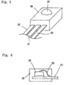
- the above resin seal 36 is heated to seal in the semiconductor element 34 and the wires 35, and thereafter, as the resin seal 36 cools down, it develops contraction stress inside itself. This causes the wires 35 to be pulled together with the resin, of which the resin seal 36 is made, in the direction of the inward contraction of the resin. On the other hand, the island 31a, on which one end of each wire 35 is stitch-bonded, contracts far less than the resin seal 36 because of their different thermal expansion coefficients.
- the wires 35 are subjected to force that pulls them in the direction of the contraction of the resin and that tends to tear the ends of the wires 35 off the island 31a, and eventually the wires 35 are broken as shown in Fig. 6. Moreover, the same can be caused even by variations in ambient temperature.
- An object of the present invention is to provide a highly reliable semiconductor device that is substantially free from wire breakage.
- a semiconductor device comprising a lead terminal having an island at one end, a semiconductor element whose bottom surface is connected to the island, one or more wires that connect the top surface of the semiconductor element to the island, and a resin seal that seals in the semiconductor element and the wires
- said island has a cut formed between a section on which said semiconductor element is mounted and a section on which said wires are bonded.
- the cut is so formed as to extend below all the wires.
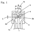
- Fig. 1 is a partly-removed plan view showing a photodetector as an example of the semiconductor device of the present invention
- Fig. 2 are partly-removed plan views each showing a modified example of the semiconductor device of the present invention
- Fig. 3 is a partly-removed plan view showing another modified example of the semiconductor device of the present invention
- Fig. 4 is a partly-removed plan view showing a conventional semiconductor device
- Fig. 5 is a perspective view of the principal portion of the conventional semiconductor device
- Fig. 6 is a diagram explaining a state of wire breakage in the conventional semiconductor device.
- a photodetector device having a semiconductor element including a photodiode element (hereinafter the semiconductor element is referred to as a photodiode element) is dealt with as an example of the semiconductor device of the present invention. This however does not suggest that application of the present invention is limited to particular types of semiconductor device.
- the semiconductor device comprises a common lead 1 (lead terminal) having at one end an approximately square-shaped island 1a, specific leads 2a and 2b formed on both sides of and approximately parallel with the common lead 1, a photodiode element 3 that is die-bonded on the island 1a, a plurality of wires 4 made of gold or other for electrically connecting the photodiode element 3 to the top surface of the island 1a and to the specific leads 2a and 2b by wire bonding, and an approximately square-shaped resin seal 5 made of epoxy resin for sealing in the photodiode element 3 and the wires 4 (the resin seal 5 actually is opaque, though it is shown as transparent in Fig. 1).
- a cut 1b is formed between the section on which the photodiode element 3 is mounted and the section on which the wires 4 are bonded.
- This cut 1b is formed along one side (the side where stitch-bonding of the wires 4 is present in the figure) of the photodiode element 3.
- the length A of the cut 1b is about 1.9 mm, and the width B of the island is about 2.3 mm. Therefore, the length A of the cut 1b is approximately 80 % of the width B of the island.
- the width C of the cut 1b is about 0.4 mm.
- the wires 4 are individually bonded at one end. Of these wires 4, four are, at the other end, stitch-bonded on the top surface of the island 1a, with the wires crossing over the cut 1b, and two are, at the other end, stitch-bonded on the specific leads 2a and 2b, respectively.
- the resin seal 5 is formed by molding epoxy resin, which is a thermosetting resin, into a shape as described earlier and as shown in Fig. 5 by use of a conventional resin-forming mold.
- the resin seal 5 is formed, for example, by applying heat-molten epoxy resin over the photodiode element 3 and the wires 4 to seal them in, and then letting the resin cool down to room temperature.
- the island 1a having a cut 1b formed between the section on which the photodiode element 3 is mounted and the section on which the wires 4 are bonded as described earlier, easily deforms in the direction (shown by arrows in Fig. 1) in which those two sections come closer to or apart from each other about the cut 1b. Accordingly, the island 1a allows its portion around the cut 1b to deform easily with the inward contraction of the epoxy resin.
- the cut 1b is so formed as to extend below all the wires 4 so that the island 1a is in a form to deform readily in the direction in which its two sections come close to or apart from each other about the cut 1b. Accordingly, the island 1a allows its portion around the cut 1b (including the portion on which the wires 4 are bonded) to deform easily with the contraction of the resin. As a result, the possibility of wire breakage is reduced significantly.
- the cut 1b is formed, as shown in Fig. 1, along one side of the square-shaped photodiode element 3 so as to be parallel with that side.
- Fig. 2 shows a cut pattern that is substantially the same as that shown in Fig. 1, and (b) to (e) show other cut patterns with which the object of the present invention is achieved.
- the cut 1b can be formed in any shape and in any position as long as the wires 4 cross over it.
- the present invention can be invariably applied to semiconductor devices having one or more wires.
- the length and width of the cut 1b are not limited to particular values as shown in the above embodiment, and it is also possible to form more than one cuts 1b.
- the cut 1b is formed with one end open, i.e. like a notch, in the above embodiment, it may be formed without an open end, i.e. as a through hole 6, as shown in Fig. 3.
- the through hole 6 needs to be large enough to allow the island to deform easily with the contraction of the epoxy resin.
- the diameter of the through hole 6 (or the major length of the hole, if it is elongated) needs to be close to the width of the island. Of course, it is also possible to form more than one such through hole 6.
- an island has a cut formed between a section on which a semiconductor element is mounted and a section on which wires are bonded.
- the semiconductor device is formed, for example, by applying heat-molten thermosetting resin over the semiconductor element and the wires so that they are sealed in in a resin seal.
- the resin as it cools down after curing, develops contraction strain inside itself. This causes the wires as well as the resin to be subjected to force that pulls them inward in the direction of the contraction.
- the island has, as described above, a cut formed between the section on which the semiconductor element is mounted and the section on which the wires are bonded, so that the island is in a form to deform readily in the direction in which its two sections come close to or away from each other about the cut. Accordingly, the island allows its portion around the cut to deform easily with the inward contraction of the resin.
- the present invention can be usefully applied to semiconductor devices including a photodiode element or any other type of semiconductor element, and is especially suitable for semiconductor devices whose semiconductor elements, lead terminals, and wires connecting these are resin-molded.
Landscapes
- Light Receiving Elements (AREA)
- Structures Or Materials For Encapsulating Or Coating Semiconductor Devices Or Solid State Devices (AREA)
- Lead Frames For Integrated Circuits (AREA)
Abstract
Description
- The present invention relates to a semiconductor device in which a semiconductor element is mounted on an island, and especially to a semiconductor device in which an island has a characteristic shape.
- Conventionally, a semiconductor device has a structure as described below. Here, a photodetector device having a semiconductor element such as a photodiode is taken as an example.
- As shown in Fig. 4, the photodetector device is composed of a
common lead 31 having at one end an approximately square-shaped island 31a,specific leads common lead 31, asemiconductor element 34 die-bonded on theisland 31a, a plurality ofwires 35 made of gold or other for electrically connecting thesemiconductor element 34 to the top surface of theisland 31a and to thespecific leads shaped resin seal 36 made of epoxy resin for sealing in thesemiconductor element 34 and the wires 35 (theresin seal 36 actually is opaque, though it is shown as transparent in Fig. 4). On the top surface of theabove semiconductor element 34 are formed a plurality of projection-like electrode pads (not shown) made of aluminum or other. On these electrode pads are bondedwires 35, of which four are, at the other end, bonded on the top surface of theisland 31a and two are, at the other end, bonded on thespecific leads island 31a so as to be grounded, and thus serve to adjust the resistance against a current flowing between thespecific leads - The
resin seal 36 is so formed as to seal in thesemiconductor element 34 and thewires 35 as shown in Fig. 5 by use of a resin-forming mold (not shown). Theresin seal 36 has, at its portion approximately above thesemiconductor device 34, ahemispherical condenser lens 37 for leading light from outside to thesemiconductor element 34. - However, this photodetector has been suffering from a following problem.
- The
above resin seal 36 is heated to seal in thesemiconductor element 34 and thewires 35, and thereafter, as theresin seal 36 cools down, it develops contraction stress inside itself. This causes thewires 35 to be pulled together with the resin, of which theresin seal 36 is made, in the direction of the inward contraction of the resin. On the other hand, theisland 31a, on which one end of eachwire 35 is stitch-bonded, contracts far less than theresin seal 36 because of their different thermal expansion coefficients. - As a result, the
wires 35 are subjected to force that pulls them in the direction of the contraction of the resin and that tends to tear the ends of thewires 35 off theisland 31a, and eventually thewires 35 are broken as shown in Fig. 6. Moreover, the same can be caused even by variations in ambient temperature. - An object of the present invention is to provide a highly reliable semiconductor device that is substantially free from wire breakage.
- According to the present invention, in a semiconductor device comprising a lead terminal having an island at one end, a semiconductor element whose bottom surface is connected to the island, one or more wires that connect the top surface of the semiconductor element to the island, and a resin seal that seals in the semiconductor element and the wires, said island has a cut formed between a section on which said semiconductor element is mounted and a section on which said wires are bonded.
- Moreover, according to the present invention, in a semiconductor device as described above, the cut is so formed as to extend below all the wires.
- Fig. 1 is a partly-removed plan view showing a photodetector as an example of the semiconductor device of the present invention; Fig. 2 are partly-removed plan views each showing a modified example of the semiconductor device of the present invention; Fig. 3 is a partly-removed plan view showing another modified example of the semiconductor device of the present invention; Fig. 4 is a partly-removed plan view showing a conventional semiconductor device; Fig. 5 is a perspective view of the principal portion of the conventional semiconductor device; and Fig. 6 is a diagram explaining a state of wire breakage in the conventional semiconductor device.
- Hereinafter, an embodiment of the present invention will be described with reference to Figs. 1 and 2. In the following descriptions, a photodetector device having a semiconductor element including a photodiode element (hereinafter the semiconductor element is referred to as a photodiode element) is dealt with as an example of the semiconductor device of the present invention. This however does not suggest that application of the present invention is limited to particular types of semiconductor device.
- As shown in Fig. 1, the semiconductor device comprises a common lead 1 (lead terminal) having at one end an approximately square-
shaped island 1a,specific leads common lead 1, aphotodiode element 3 that is die-bonded on theisland 1a, a plurality ofwires 4 made of gold or other for electrically connecting thephotodiode element 3 to the top surface of theisland 1a and to thespecific leads shaped resin seal 5 made of epoxy resin for sealing in thephotodiode element 3 and the wires 4 (theresin seal 5 actually is opaque, though it is shown as transparent in Fig. 1). - In the
island 1a, acut 1b is formed between the section on which thephotodiode element 3 is mounted and the section on which thewires 4 are bonded. Thiscut 1b is formed along one side (the side where stitch-bonding of thewires 4 is present in the figure) of thephotodiode element 3. The length A of thecut 1b is about 1.9 mm, and the width B of the island is about 2.3 mm. Therefore, the length A of thecut 1b is approximately 80 % of the width B of the island. The width C of thecut 1b is about 0.4 mm. Moreover, on the top surface of thephotodiode element 3, six electrode pads (not shown) made of aluminum are formed, and, on these electrode pads, thewires 4 are individually bonded at one end. Of thesewires 4, four are, at the other end, stitch-bonded on the top surface of theisland 1a, with the wires crossing over thecut 1b, and two are, at the other end, stitch-bonded on thespecific leads - In the photodetector device having the above structure, the
resin seal 5 is formed by molding epoxy resin, which is a thermosetting resin, into a shape as described earlier and as shown in Fig. 5 by use of a conventional resin-forming mold. - Specifically, the
resin seal 5 is formed, for example, by applying heat-molten epoxy resin over thephotodiode element 3 and thewires 4 to seal them in, and then letting the resin cool down to room temperature. - However, as the epoxy resin cools down after heat curing, it develops contraction stress inside itself. This causes the
wires 4 as well as the epoxy resin to be subjected to force that pulls them inward in the direction of the contraction. On the other hand, theisland 1a, having acut 1b formed between the section on which thephotodiode element 3 is mounted and the section on which thewires 4 are bonded as described earlier, easily deforms in the direction (shown by arrows in Fig. 1) in which those two sections come closer to or apart from each other about thecut 1b. Accordingly, theisland 1a allows its portion around thecut 1b to deform easily with the inward contraction of the epoxy resin. - As a result, when the
wires 4 are pulled, at their ends bonded on theisland 1a, in the direction in which the epoxy resin contracts, theisland 1a is also pulled in the same direction in which the epoxy resin contracts. Thus, the possibility of breakage of the wires at their ends bonded on theisland 1a can be reduced significantly. - In this embodiment, the
cut 1b is so formed as to extend below all thewires 4 so that theisland 1a is in a form to deform readily in the direction in which its two sections come close to or apart from each other about thecut 1b. Accordingly, theisland 1a allows its portion around thecut 1b (including the portion on which thewires 4 are bonded) to deform easily with the contraction of the resin. As a result, the possibility of wire breakage is reduced significantly. - In the above embodiment, the
cut 1b is formed, as shown in Fig. 1, along one side of the square-shaped photodiode element 3 so as to be parallel with that side. However, this does not suggest any limitation to the way thecut 1b is formed. In Fig. 2, (a) shows a cut pattern that is substantially the same as that shown in Fig. 1, and (b) to (e) show other cut patterns with which the object of the present invention is achieved. In short, thecut 1b can be formed in any shape and in any position as long as thewires 4 cross over it. Moreover, although there are fourwires 4 crossing over thecut 1b in the above embodiment, the present invention can be invariably applied to semiconductor devices having one or more wires. - Furthermore, the length and width of the
cut 1b are not limited to particular values as shown in the above embodiment, and it is also possible to form more than onecuts 1b. - Moreover, although the
cut 1b is formed with one end open, i.e. like a notch, in the above embodiment, it may be formed without an open end, i.e. as a throughhole 6, as shown in Fig. 3. In this case, however, in order to achieve the object of the present invention, the throughhole 6 needs to be large enough to allow the island to deform easily with the contraction of the epoxy resin. Specifically, the diameter of the through hole 6 (or the major length of the hole, if it is elongated) needs to be close to the width of the island. Of course, it is also possible to form more than one such throughhole 6. - Furthermore, although a photodetector device is taken as an example of a semiconductor device in the above embodiment, this does not suggest that application of the present invention is limited to particular types of semiconductor device.
- In a semiconductor device according to the present invention, an island has a cut formed between a section on which a semiconductor element is mounted and a section on which wires are bonded. This offers the following advantages.
- The semiconductor device is formed, for example, by applying heat-molten thermosetting resin over the semiconductor element and the wires so that they are sealed in in a resin seal. The resin, as it cools down after curing, develops contraction strain inside itself. This causes the wires as well as the resin to be subjected to force that pulls them inward in the direction of the contraction. On the other hand, the island has, as described above, a cut formed between the section on which the semiconductor element is mounted and the section on which the wires are bonded, so that the island is in a form to deform readily in the direction in which its two sections come close to or away from each other about the cut. Accordingly, the island allows its portion around the cut to deform easily with the inward contraction of the resin.
- As a result, when the wires are pulled, at their ends bonded on the island, in the direction in which the epoxy resin contracts, the
island 1a is also pulled in the same direction in which the epoxy resin contracts. Thus, the possibility of breakage of the wires at their ends bonded on theisland 1a can be reduced significantly. - As described above, the present invention can be usefully applied to semiconductor devices including a photodiode element or any other type of semiconductor element, and is especially suitable for semiconductor devices whose semiconductor elements, lead terminals, and wires connecting these are resin-molded.
Claims (6)
- A semiconductor device comprising a lead terminal that has an island at one end, a semiconductor element whose bottom surface is mounted on the island, one or more wires that connect a top surface of the semiconductor element to the island, and a resin seal that seals in the semiconductor device and the wires,
wherein said island has a cut formed between a section on which said semiconductor element is mounted and a section on which said wires are bonded. - A semiconductor device as claimed in claim 1,
wherein said cut is so formed as to extend below all of said wires. - A semiconductor device as claimed in claim 1,
wherein said resin is epoxy resin. - A semiconductor device as claimed in claim 1,
wherein said semiconductor element is square-shaped and said cut is formed along one side of the semiconductor element, and wherein said wires that are at one end connected to said semiconductor element are stitch-bonded on a top surface of said island such that the wires cross over the cut. - A semiconductor device as claimed in claim 4,
wherein said cut is formed to have a length equal to approximately 80% of a width of said island. - A semiconductor device comprising a lead terminal that has an island at one end, a semiconductor element whose bottom surface is mounted on the island, one or more wires that connect a top surface of the semiconductor element to the island, and a resin seal that seals in the semiconductor device and the wires,
wherein said island has a through hole formed between a section on which said semiconductor element is mounted and a section on which said wires are bonded.
Applications Claiming Priority (7)
| Application Number | Priority Date | Filing Date | Title |
|---|---|---|---|
| JP113303/95 | 1995-05-11 | ||
| JP11330395 | 1995-05-11 | ||
| JP11330395 | 1995-05-11 | ||
| JP10572596A JP3907743B2 (en) | 1995-05-11 | 1996-04-25 | Semiconductor device |
| JP105725/96 | 1996-04-25 | ||
| JP10572596 | 1996-04-25 | ||
| PCT/JP1996/001267 WO1996036074A1 (en) | 1995-05-11 | 1996-05-10 | Semiconductor device |
Publications (3)
| Publication Number | Publication Date |
|---|---|
| EP0771027A1 true EP0771027A1 (en) | 1997-05-02 |
| EP0771027A4 EP0771027A4 (en) | 2000-01-05 |
| EP0771027B1 EP0771027B1 (en) | 2005-10-26 |
Family
ID=26445967
Family Applications (1)
| Application Number | Title | Priority Date | Filing Date |
|---|---|---|---|
| EP96913744A Expired - Lifetime EP0771027B1 (en) | 1995-05-11 | 1996-05-10 | Semiconductor device |
Country Status (8)
| Country | Link |
|---|---|
| US (1) | US6242801B1 (en) |
| EP (1) | EP0771027B1 (en) |
| JP (1) | JP3907743B2 (en) |
| KR (1) | KR100370550B1 (en) |
| CN (1) | CN1134073C (en) |
| DE (1) | DE69635334T2 (en) |
| TW (1) | TW301046B (en) |
| WO (1) | WO1996036074A1 (en) |
Families Citing this family (3)
| Publication number | Priority date | Publication date | Assignee | Title |
|---|---|---|---|---|
| JP4198284B2 (en) * | 1999-10-07 | 2008-12-17 | ローム株式会社 | Optical semiconductor device for surface mounting |
| JP2002353383A (en) * | 2001-05-30 | 2002-12-06 | Moric Co Ltd | Semiconductor device |
| JP3913574B2 (en) * | 2002-02-27 | 2007-05-09 | 三洋電機株式会社 | Semiconductor device |
Family Cites Families (24)
| Publication number | Priority date | Publication date | Assignee | Title |
|---|---|---|---|---|
| JPS52129379A (en) * | 1976-04-23 | 1977-10-29 | Hitachi Ltd | Plastic molded semiconductor device |
| JPS55120152A (en) * | 1979-03-09 | 1980-09-16 | Fujitsu Ltd | Semiconductor device |
| JPS57154863A (en) * | 1981-03-19 | 1982-09-24 | Fujitsu Ltd | Manufacture of resin sealing type electronic parts |
| JPS6234154A (en) | 1985-08-08 | 1987-02-14 | Oji Paper Co Ltd | Support for photographic printing paper |
| JPH06101579B2 (en) * | 1986-08-22 | 1994-12-12 | 松下電工株式会社 | Photo coupler manufacturing method |
| JPH0625978B2 (en) | 1987-11-09 | 1994-04-06 | 日本電気株式会社 | Mutual monitoring control method |
| JPH01123356U (en) * | 1988-02-16 | 1989-08-22 | ||
| JPH01312858A (en) * | 1988-06-10 | 1989-12-18 | Nec Corp | Resin sealed semiconductor device |
| JPH02191378A (en) * | 1988-10-25 | 1990-07-27 | Omron Tateisi Electron Co | Photoelectric element, manufacture thereof and drive device therefor |
| JPH02159750A (en) * | 1988-12-13 | 1990-06-19 | Nec Corp | Manufacture of semiconductor device |
| JPH04280664A (en) * | 1990-10-18 | 1992-10-06 | Texas Instr Inc <Ti> | Lead fram for semiconductor device |
| JPH04262560A (en) * | 1991-02-18 | 1992-09-17 | Mitsubishi Electric Corp | Resin-sealed field effect semiconductor device and manufacture thereof |
| JPH05109959A (en) * | 1991-10-17 | 1993-04-30 | Nec Corp | Manufacture of semiconductor device |
| JP3167769B2 (en) * | 1992-01-16 | 2001-05-21 | シャープ株式会社 | Lead frame and method of manufacturing optical device using the same |
| JP2708320B2 (en) * | 1992-04-17 | 1998-02-04 | 三菱電機株式会社 | Multi-chip type semiconductor device and manufacturing method thereof |
| JP2805563B2 (en) * | 1992-08-07 | 1998-09-30 | シャープ株式会社 | Reflection type optical coupling device and method of manufacturing the same |
| JP2695736B2 (en) * | 1992-12-11 | 1998-01-14 | 三菱電機株式会社 | Resin-encapsulated semiconductor device and method for manufacturing lead frame provided with its resistance wire |
| JPH06216307A (en) * | 1993-01-13 | 1994-08-05 | Mitsubishi Electric Corp | Resin-sealed semiconductor device |
| JPH06244430A (en) * | 1993-02-16 | 1994-09-02 | Fuji Electric Co Ltd | Semiconductor device |
| JP2500785B2 (en) * | 1993-09-20 | 1996-05-29 | 日本電気株式会社 | Film carrier tape for semiconductor package and semiconductor device using the same |
| JP2701712B2 (en) * | 1993-11-11 | 1998-01-21 | 日本電気株式会社 | Semiconductor device |
| JPH08139113A (en) * | 1994-11-09 | 1996-05-31 | Mitsubishi Electric Corp | Resin-sealed semiconductor device |
| US5491360A (en) * | 1994-12-28 | 1996-02-13 | National Semiconductor Corporation | Electronic package for isolated circuits |
| JP3429921B2 (en) * | 1995-10-26 | 2003-07-28 | 三菱電機株式会社 | Semiconductor device |
-
1996
- 1996-04-25 JP JP10572596A patent/JP3907743B2/en not_active Expired - Fee Related
- 1996-05-10 WO PCT/JP1996/001267 patent/WO1996036074A1/en not_active Ceased
- 1996-05-10 US US08/750,974 patent/US6242801B1/en not_active Expired - Fee Related
- 1996-05-10 CN CNB96190481XA patent/CN1134073C/en not_active Expired - Fee Related
- 1996-05-10 KR KR1019970700116A patent/KR100370550B1/en not_active Expired - Fee Related
- 1996-05-10 EP EP96913744A patent/EP0771027B1/en not_active Expired - Lifetime
- 1996-05-10 DE DE69635334T patent/DE69635334T2/en not_active Expired - Fee Related
- 1996-05-11 TW TW085105585A patent/TW301046B/zh active
Also Published As
| Publication number | Publication date |
|---|---|
| DE69635334T2 (en) | 2006-07-20 |
| CN1134073C (en) | 2004-01-07 |
| WO1996036074A1 (en) | 1996-11-14 |
| KR100370550B1 (en) | 2003-07-18 |
| EP0771027B1 (en) | 2005-10-26 |
| JP3907743B2 (en) | 2007-04-18 |
| EP0771027A4 (en) | 2000-01-05 |
| DE69635334D1 (en) | 2005-12-01 |
| US6242801B1 (en) | 2001-06-05 |
| CN1154180A (en) | 1997-07-09 |
| JPH0927577A (en) | 1997-01-28 |
| TW301046B (en) | 1997-03-21 |
| KR970705180A (en) | 1997-09-06 |
Similar Documents
| Publication | Publication Date | Title |
|---|---|---|
| US6177721B1 (en) | Chip stack-type semiconductor package and method for fabricating the same | |
| KR980006163A (en) | Resin Sealed Semiconductor Device and Manufacturing Method Thereof | |
| KR970018432A (en) | Semiconductor device with lead on chip structure | |
| JP3754471B2 (en) | Package / lead frame for optical coupler and manufacturing method thereof | |
| US5479050A (en) | Leadframe with pedestal | |
| KR100200377B1 (en) | Electronic component and manufacturing method | |
| US20030116834A1 (en) | High density direct connect LOC assembly | |
| US5780923A (en) | Modified bus bar with Kapton™ tape or insulative material on LOC packaged part | |
| CN1169032A (en) | Lead frame and semiconductor package | |
| US6242801B1 (en) | Semiconductor device | |
| US6541856B2 (en) | Thermally enhanced high density semiconductor package | |
| JPH0286184A (en) | optoelectronic device | |
| USH73H (en) | Integrated circuit packages | |
| JP7292241B2 (en) | Semiconductor device and its manufacturing method | |
| JP3183715B2 (en) | Resin-sealed optical element | |
| KR100220244B1 (en) | Stack Package with Solder Bump | |
| EP0410116B1 (en) | Method of manufacturing a wire-bonded semiconductor device | |
| KR100221918B1 (en) | Chip scale package | |
| KR200211272Y1 (en) | Chip size package | |
| KR100336761B1 (en) | Stacked buttom lead package and manufacturing method thereof | |
| JPS59198744A (en) | Resin sealed type semiconductor device | |
| KR200164518Y1 (en) | Semiconductor package | |
| JPS61276273A (en) | Switching element | |
| JP2528023Y2 (en) | Optical coupling device | |
| KR940006582B1 (en) | Ceramic semiconductor package structure and manufacturing method |
Legal Events
| Date | Code | Title | Description |
|---|---|---|---|
| PUAI | Public reference made under article 153(3) epc to a published international application that has entered the european phase |
Free format text: ORIGINAL CODE: 0009012 |
|
| AK | Designated contracting states |
Kind code of ref document: A1 Designated state(s): DE FR GB IT |
|
| 17P | Request for examination filed |
Effective date: 19970506 |
|
| A4 | Supplementary search report drawn up and despatched |
Effective date: 19991124 |
|
| AK | Designated contracting states |
Kind code of ref document: A4 Designated state(s): DE FR GB IT |
|
| RIC1 | Information provided on ipc code assigned before grant |
Free format text: 7H 01L 23/48 A, 7H 01L 23/495 B |
|
| 17Q | First examination report despatched |
Effective date: 20030319 |
|
| GRAP | Despatch of communication of intention to grant a patent |
Free format text: ORIGINAL CODE: EPIDOSNIGR1 |
|
| GRAS | Grant fee paid |
Free format text: ORIGINAL CODE: EPIDOSNIGR3 |
|
| GRAA | (expected) grant |
Free format text: ORIGINAL CODE: 0009210 |
|
| AK | Designated contracting states |
Kind code of ref document: B1 Designated state(s): DE FR GB IT |
|
| PG25 | Lapsed in a contracting state [announced via postgrant information from national office to epo] |
Ref country code: IT Free format text: LAPSE BECAUSE OF FAILURE TO SUBMIT A TRANSLATION OF THE DESCRIPTION OR TO PAY THE FEE WITHIN THE PRE;WARNING: LAPSES OF ITALIAN PATENTS WITH EFFECTIVE DATE BEFORE 2007 MAY HAVE OCCURRED AT ANY TIME BEFORE 2007. THE CORRECT EFFECTIVE DATE MAY BE DIFFERENT FROM THE ONE RECORDED.SCRIBED TIME-LIMIT Effective date: 20051026 |
|
| REG | Reference to a national code |
Ref country code: GB Ref legal event code: FG4D |
|
| REF | Corresponds to: |
Ref document number: 69635334 Country of ref document: DE Date of ref document: 20051201 Kind code of ref document: P |
|
| ET | Fr: translation filed | ||
| PLBE | No opposition filed within time limit |
Free format text: ORIGINAL CODE: 0009261 |
|
| STAA | Information on the status of an ep patent application or granted ep patent |
Free format text: STATUS: NO OPPOSITION FILED WITHIN TIME LIMIT |
|
| 26N | No opposition filed |
Effective date: 20060727 |
|
| PGFP | Annual fee paid to national office [announced via postgrant information from national office to epo] |
Ref country code: DE Payment date: 20080724 Year of fee payment: 13 |
|
| PGFP | Annual fee paid to national office [announced via postgrant information from national office to epo] |
Ref country code: GB Payment date: 20080522 Year of fee payment: 13 |
|
| GBPC | Gb: european patent ceased through non-payment of renewal fee |
Effective date: 20090510 |
|
| REG | Reference to a national code |
Ref country code: FR Ref legal event code: ST Effective date: 20100129 |
|
| PG25 | Lapsed in a contracting state [announced via postgrant information from national office to epo] |
Ref country code: FR Free format text: LAPSE BECAUSE OF NON-PAYMENT OF DUE FEES Effective date: 20090602 |
|
| PGFP | Annual fee paid to national office [announced via postgrant information from national office to epo] |
Ref country code: FR Payment date: 20080519 Year of fee payment: 13 |
|
| PG25 | Lapsed in a contracting state [announced via postgrant information from national office to epo] |
Ref country code: GB Free format text: LAPSE BECAUSE OF NON-PAYMENT OF DUE FEES Effective date: 20090510 |
|
| PG25 | Lapsed in a contracting state [announced via postgrant information from national office to epo] |
Ref country code: DE Free format text: LAPSE BECAUSE OF NON-PAYMENT OF DUE FEES Effective date: 20091201 |