EP0769754B1 - Capteur monolithique d'empreintes digitales - Google Patents
Capteur monolithique d'empreintes digitales Download PDFInfo
- Publication number
- EP0769754B1 EP0769754B1 EP96402200A EP96402200A EP0769754B1 EP 0769754 B1 EP0769754 B1 EP 0769754B1 EP 96402200 A EP96402200 A EP 96402200A EP 96402200 A EP96402200 A EP 96402200A EP 0769754 B1 EP0769754 B1 EP 0769754B1
- Authority
- EP
- European Patent Office
- Prior art keywords
- layer
- pressure
- microsensors
- fingerprint sensor
- microsensor
- Prior art date
- Legal status (The legal status is an assumption and is not a legal conclusion. Google has not performed a legal analysis and makes no representation as to the accuracy of the status listed.)
- Expired - Lifetime
Links
Images

Classifications
-
- A—HUMAN NECESSITIES
- A61—MEDICAL OR VETERINARY SCIENCE; HYGIENE
- A61B—DIAGNOSIS; SURGERY; IDENTIFICATION
- A61B5/00—Measuring for diagnostic purposes; Identification of persons
- A61B5/117—Identification of persons
- A61B5/1171—Identification of persons based on the shapes or appearances of their bodies or parts thereof
- A61B5/1172—Identification of persons based on the shapes or appearances of their bodies or parts thereof using fingerprinting
-
- G—PHYSICS
- G01—MEASURING; TESTING
- G01L—MEASURING FORCE, STRESS, TORQUE, WORK, MECHANICAL POWER, MECHANICAL EFFICIENCY, OR FLUID PRESSURE
- G01L1/00—Measuring force or stress, in general
- G01L1/20—Measuring force or stress, in general by measuring variations in ohmic resistance of solid materials or of electrically-conductive fluids; by making use of electrokinetic cells, i.e. liquid-containing cells wherein an electrical potential is produced or varied upon the application of stress
- G01L1/205—Measuring force or stress, in general by measuring variations in ohmic resistance of solid materials or of electrically-conductive fluids; by making use of electrokinetic cells, i.e. liquid-containing cells wherein an electrical potential is produced or varied upon the application of stress using distributed sensing elements
-
- G—PHYSICS
- G01—MEASURING; TESTING
- G01L—MEASURING FORCE, STRESS, TORQUE, WORK, MECHANICAL POWER, MECHANICAL EFFICIENCY, OR FLUID PRESSURE
- G01L9/00—Measuring steady of quasi-steady pressure of fluid or fluent solid material by electric or magnetic pressure-sensitive elements; Transmitting or indicating the displacement of mechanical pressure-sensitive elements, used to measure the steady or quasi-steady pressure of a fluid or fluent solid material, by electric or magnetic means
- G01L9/0041—Transmitting or indicating the displacement of flexible diaphragms
- G01L9/0042—Constructional details associated with semiconductive diaphragm sensors, e.g. etching, or constructional details of non-semiconductive diaphragms
-
- G—PHYSICS
- G06—COMPUTING OR CALCULATING; COUNTING
- G06V—IMAGE OR VIDEO RECOGNITION OR UNDERSTANDING
- G06V40/00—Recognition of biometric, human-related or animal-related patterns in image or video data
- G06V40/10—Human or animal bodies, e.g. vehicle occupants or pedestrians; Body parts, e.g. hands
- G06V40/12—Fingerprints or palmprints
- G06V40/13—Sensors therefor
- G06V40/1306—Sensors therefor non-optical, e.g. ultrasonic or capacitive sensing
Definitions
- the invention relates to the field of authenticating people through the recognition of their fingerprints.
- the traditional method to use this peculiarity of nature is a printing method ink-based. It consists of pressing the finger on an inked surface and put this finger on a surface of white paper.
- the ridge lines press on the white surface more than the valleys; the ink of ridge lines carries better on paper than that of the valleys, and a drawing of the ridge lines appears clearly on the white surface.
- This traditional method is not pleasant for the person who has to ink his finger and clean up after; and it does not directly allow a automatic image recognition processing.
- US Patent 4,577,345 describes a method and a fingerprint capture and identification device using a network of contact points on a chip integrated circuit.
- Occasional electrical contacts may be established at each point of the network by simply pressing the above this point.
- Ridge lines of fingerprints exert higher pressure than the valleys, and therefore, finger pressure can establish a pattern of electrical contacts corresponding to the lines ridge, while the valleys define a pattern without contact points.
- the pattern thus drawn can be detected by a network of transistors connected to the contact points possible.
- a conductive membrane flexible is stretched over the top surface of the integrated circuit and bonded over the entire periphery of this one. It is she who makes the contacts at each point of the network depending on the pressure pattern exerted by the finger.
- the membrane assembly in particular is an operation that does not belong to the technology of integrated circuits and which is difficult to produce. The production cost therefore remains high.
- the subject of the invention is a fingerprint sensor which does not have the disadvantages encountered in the prior art.
- a sensor is proposed. fingerprint which includes a means of detection pressure sensitive to the pattern of the imprint and electronic circuits coupled to this detection means and to provide electrical signals representing this motif.
- This sensor is monolithic (without insert) and produced entirely according to a integrated circuit manufacturing technology electronic as well for the way of detecting pressure than for electronic circuits coupled to this way.
- Integrated circuit manufacturing technologies are thin layer deposition techniques, photolithography and dry or wet etching of these layers, possible doping with impurities, and various heat treatments. They are performed in batches on slices comprising several identical integrated circuits.
- the fingerprint sensor therefore consists of a single integrated circuit which brings together all functions necessary to transform the reliefs of finger skin (ridges and valleys) in signals electrics which are preferably emitted in the form digital (sequence of binary signals).
- the component according to the invention is preferably performed according to a standard CMOS process and currently using micro-machining techniques well controlled. No assembly of parts made separately is not necessary.
- the fingerprint sensor will constitute the point entry of an identification system and / or fingerprint authentication installed on a personal computer (PC) or on a workstation connected to a central computer.
- PC personal computer
- workstation connected to a central computer.
- the system reconstructs the image of the footprint using the coordinates (X, Y) of each point of the pattern identified by means of pressure detection.
- the computer provides signals to the sensor control such as a clock, a signal reset.
- the sensor being in matrix principle, the microcomputer can control point-by-point access to the different points of the matrix.
- the points of the matrix are pressure microsensors, all microsensors providing an overall matrix image of the pattern pressure resulting from the application of the finger on the sensor.
- the computer receives a signal from the sensor measurement representing the pressure at each point, and the correlates with count signals representing the position of this point in an image frame.
- the established image can be processed by a specialized algorithm and compared to other images stored in a database.
- the invention therefore relates to a sensor fingerprint including a matrix of pressure microsensors (12) sensitive to the pattern of the fingerprint the sensor being made on a substrate according to a manufacturing technology of integrated circuit, mainly characterized in that each microsensor in the matrix includes a cavity (44) closed by a diaphragm (46) consisting of a insulating material for carrying conductive elements of the microsensor and allow their deformations under the action of pressure.
- the pressure microsensors operate according to an effect piezoresistive: these are resistors whose value varies with the pressure exerted.
- each pressure microsensor consists of a microswitch.
- each microsensor pressure element consists of a variable capacity.
- the microsensors are formed by a resistance bridge piezo deposited on a diaphragm stretched over a cavity. Deformation of the diaphragm, under the effect of the pressure, causes the deformation of the resistances and therefore a variation of their values.
- the microsensor is made up of two distant metal layers forming either the armatures of the variable capacitor, either the terminals of the microswitch, and a layer insulation (36) stretched over a cavity and forming a diaphragm, the upper reinforcement being integral with this diaphragm.
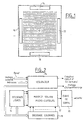
- Figure 1 we see the constitution general of a sensor according to the invention. It comprises basically a matrix of 128x128 elements individual that are pressure microsensors arranged in a network of rows and columns.
- Each element occupies a square surface about 50 microns by 50 microns, or one circle of approximately 50 micrometers in diameter.
- the pitch of the network is preferably at most 65 micrometers, that is, the centers of two adjacent elements are separated by 65 micrometers at plus: the overall surface of the matrix is 8.3x8.3 square millimeters, sufficient to grasp the part central of a fingerprint, which is the area richer in information.
- the dimensions given above correspond to an exemplary embodiment; they give a sufficiently precise definition of footprint and are technologically feasible without particular problem.
- the microsensors can be produced according to several techniques, using physical effects different for pressure detection.
- the sensors can operate on a capacitive effect, or an effect piezoelectric, or a simple integrated micro-switch in the monolithic circuit.
- Each element can contain electronics simple allowing, by comparison with a threshold, to transform the pressure variation into a logic level binary.
- the detection electronics is the easier to do.
- Binary information is manufactured in the microsensor itself (the switch closed or open depending on the presence or absence of a pressure).
- Figure 2 shows the electrical diagram of the fingerprint sensor.
- the sequencer 14 receives the reset signal (reset), a clock external, and possibly addresses for point-by-point or line-by-line exploration of the matrix image collected by the microsensors; the image can however be transmitted outside the integrated circuit by systematic line-by-line scanning line analog to a video image scan, the sequencer then comprising the circuit elements necessary to perform this scan.
- the sequencer transmits the line addresses and from column to row and column decoders (16 and 18) which allow point-to-point access to matrix 12 pressure microsensors.
- the signal electric from a microsensor addressed by these decoders is transmitted on a sensor output monolithic, through the output stage 20.
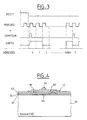
- Figure 3 shows the output signals of the sensor, and associated control signals.
- the signal Reset defines the start of a systematic exploration of the matrix.
- the clock defines the pace of exploration (by example a clock tick for each point of the matrix); successive addresses are incremented, for example line by line; for a 128x128 matrix There are 16,384 successive addresses to explore.
- the frame counter provides a reset pulse to zero to define each new transmission start of a complete picture.
- the output signals transmitted are binary signals representing the exceeding or not exceeding of a pressure threshold at each point of the matrix.
- the signals can be transmitted in series or in parallel by words of 8 bits, 16 bits or more.
- the output signal is analog.
- CMOS circuits When entering a fingerprint, the sensor comes into direct contact with a hostile environment. It must therefore be protected. Besides a layer of passivation which completes the manufacturing process CMOS circuits, a flexible layer (of silicone for example) as final protection.
- This layer can also be used for improve the pressure transfer function between the finger and microsensors. In this case, we can make an extra thickness in this layer at center of each microsensor, also to improve this transfer function.
- Figure 4 shows a section of such structure with a flexible protective layer 32 deposited on the surface of a circuit substrate integrated 30 in which were previously made pressure microsensors and all electronics corresponding signal processing.
- Layer 32 has, in the center of each microsensor, an extra thickness forming a pad central 34.
- the additional thickness can be obtained by deposit successive of two layers, the first being uniform and the second being deposited through a mask delimiting the studs in excess thickness.
- the material of layer 32 is preferably silicone, both flexible and resistant.
- the following example gives an embodiment detailed for pressure microsensors using a piezoresistive effect.
- the process is compatible with CMOS technology and therefore allows integration on the same microsensors integrated circuit chip and electronic control and processing circuits signal.
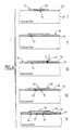
- FIG. 5 gives the main stages of production.
- a layer is deposited sacrificial or sacrificial layer of silicon polycrystalline 35.
- This layer is photo-etched to leave remain a polycrystalline silicon zone at the location of each microsensor.
- nitride of silicon 36 over the entire surface of the substrate, then a second layer of polycrystalline silicon 38.
- This second layer is etched to make bridges of piezoelectric resistors (a Weathstone bridge of 4 resistors) each corresponding to a microsensor pressure.
- One or more resistors of a bridge are deposited above the polycrystalline silicon zones of the first layer. Then a second layer of silicon nitride 40 is deposited to protect the resistances.
- the next step is to practice holes 42 in the layers of silicon nitride, at side of the resistors but above the areas of the first layer of polycrystalline silicon 35.
- KOH wet etching
- a cavity 44 then remains under the piezoelectric resistors which are then suspended on a stretched insulating layer and which can undergo deformations when pressure is exerted on them.
- the stretched insulating layer is here constituted by the layers of silicon nitride 36 and 40 forming a diaphragm 46 suspended above the cavity 44.
- the side walls of the cavity are made of nitride silicon.
- the bottom consists of the thin layer etching stop 33 resting on the substrate.
- the electronic control and treatment are formed simultaneously by operations classic CMOS deposition and engraving, some of the above steps being common with steps for making CMOS circuits, and all anyway being compatible with the creation of CMOS circuits on the same substrate.
- the flexible protective layer 32 (FIG. 4) in silicone or similar material is deposited at the end of process, after the final passivation steps (layers of silica or others) conventional in integrated circuits.
- the following example gives an embodiment detailed microsensor pressure using a capacitive effect or microswitches.
- the realization process is the same, only the thickness of the diaphragm changes to allow or not establishing contact.
- An order of magnitude of this thickness is 0.5 ⁇ m.
- a metal layer for example Au or Ti which will used either as the first reinforcement 51 of a capacity variable, either as the first bound of a microswitch.
- This layer 51 is etched to form the geometry (circular in this embodiment) and the location of the frame.
- the diaphragm 46 and the frame 52 are concentric.
- a second layer of metal 52 (Au or Ti) is deposited to form either the second capacity frame, the second microswitch terminal. This layer is etched for leave the second frame in the vertical alignment of the first.
- the second step is to deposit a layer 36 fine silicon nitride over the entire surface of the substrate.
- the third step is to practice a hole on the edge of the diaphragm 36 and which crosses the layer nitride to reach the sacrificed layer. Then, wet etching is performed on the substrate. The solution attacks the sacrificial layer through the hole. The engraving continues until the complete disappearance of the sacrificed layer. A cavity is therefore formed. The diaphragm 46 and upper frame 52 are located completely cleared.
- a deposit is made of silicon nitride 48 under vacuum to close the hole and seal the cavity (plug 48).
- the last step is to deposit a layer of silicone 32 to protect the assembly and achieve pad centered in the middle of each microsensor (step V).
Landscapes
- Engineering & Computer Science (AREA)
- Physics & Mathematics (AREA)
- Health & Medical Sciences (AREA)
- General Physics & Mathematics (AREA)
- Life Sciences & Earth Sciences (AREA)
- Surgery (AREA)
- General Health & Medical Sciences (AREA)
- Multimedia (AREA)
- Biophysics (AREA)
- Pathology (AREA)
- Biomedical Technology (AREA)
- Heart & Thoracic Surgery (AREA)
- Medical Informatics (AREA)
- Molecular Biology (AREA)
- Human Computer Interaction (AREA)
- Animal Behavior & Ethology (AREA)
- Theoretical Computer Science (AREA)
- Public Health (AREA)
- Veterinary Medicine (AREA)
- Chemical & Material Sciences (AREA)
- Analytical Chemistry (AREA)
- Image Input (AREA)
- Pressure Sensors (AREA)
- Measurement Of Length, Angles, Or The Like Using Electric Or Magnetic Means (AREA)
- Measuring Fluid Pressure (AREA)
- Force Measurement Appropriate To Specific Purposes (AREA)
- Semiconductor Integrated Circuits (AREA)
- Measurement Of The Respiration, Hearing Ability, Form, And Blood Characteristics Of Living Organisms (AREA)
Applications Claiming Priority (2)
| Application Number | Priority Date | Filing Date | Title |
|---|---|---|---|
| FR9512168 | 1995-10-17 | ||
| FR9512168A FR2739977B1 (fr) | 1995-10-17 | 1995-10-17 | Capteur monolithique d'empreintes digitales |
Publications (2)
| Publication Number | Publication Date |
|---|---|
| EP0769754A1 EP0769754A1 (fr) | 1997-04-23 |
| EP0769754B1 true EP0769754B1 (fr) | 2000-05-24 |
Family
ID=9483604
Family Applications (1)
| Application Number | Title | Priority Date | Filing Date |
|---|---|---|---|
| EP96402200A Expired - Lifetime EP0769754B1 (fr) | 1995-10-17 | 1996-10-15 | Capteur monolithique d'empreintes digitales |
Country Status (5)
| Country | Link |
|---|---|
| US (1) | US5844287A (enExample) |
| EP (1) | EP0769754B1 (enExample) |
| JP (1) | JPH09126918A (enExample) |
| DE (1) | DE69608521T2 (enExample) |
| FR (1) | FR2739977B1 (enExample) |
Families Citing this family (94)
| Publication number | Priority date | Publication date | Assignee | Title |
|---|---|---|---|---|
| US5658698A (en) * | 1994-01-31 | 1997-08-19 | Canon Kabushiki Kaisha | Microstructure, process for manufacturing thereof and devices incorporating the same |
| US7882032B1 (en) | 1994-11-28 | 2011-02-01 | Open Invention Network, Llc | System and method for tokenless biometric authorization of electronic communications |
| US6950810B2 (en) | 1994-11-28 | 2005-09-27 | Indivos Corporation | Tokenless biometric electronic financial transactions via a third party identicator |
| US7613659B1 (en) | 1994-11-28 | 2009-11-03 | Yt Acquisition Corporation | System and method for processing tokenless biometric electronic transmissions using an electronic rule module clearinghouse |
| US7248719B2 (en) | 1994-11-28 | 2007-07-24 | Indivos Corporation | Tokenless electronic transaction system |
| US7631193B1 (en) | 1994-11-28 | 2009-12-08 | Yt Acquisition Corporation | Tokenless identification system for authorization of electronic transactions and electronic transmissions |
| US20040128249A1 (en) | 1994-11-28 | 2004-07-01 | Indivos Corporation, A Delaware Corporation | System and method for tokenless biometric electronic scrip |
| FR2762389B1 (fr) * | 1997-04-17 | 1999-05-21 | Commissariat Energie Atomique | Microsysteme a membrane souple pour capteur de pression et procede de realisation |
| US6088585A (en) * | 1997-05-16 | 2000-07-11 | Authentec, Inc. | Portable telecommunication device including a fingerprint sensor and related methods |
| JP3592487B2 (ja) * | 1997-07-02 | 2004-11-24 | 日本電信電話株式会社 | 指紋認識集積回路 |
| US6240199B1 (en) * | 1997-07-24 | 2001-05-29 | Agere Systems Guardian Corp. | Electronic apparatus having improved scratch and mechanical resistance |
| JP3053007B2 (ja) * | 1997-07-28 | 2000-06-19 | 日本電気株式会社 | 指紋センサ |
| JP3102395B2 (ja) * | 1997-11-27 | 2000-10-23 | 日本電気株式会社 | 指紋検出装置 |
| US6317508B1 (en) * | 1998-01-13 | 2001-11-13 | Stmicroelectronics, Inc. | Scanning capacitive semiconductor fingerprint detector |
| US5982608A (en) * | 1998-01-13 | 1999-11-09 | Stmicroelectronics, Inc. | Semiconductor variable capacitor |
| EP0940652B1 (en) * | 1998-03-05 | 2004-12-22 | Nippon Telegraph and Telephone Corporation | Surface shape recognition sensor and method of fabricating the same |
| JP3873454B2 (ja) * | 1998-05-29 | 2007-01-24 | 株式会社デンソー | 半導体圧力センサ |
| US6131464A (en) * | 1998-06-16 | 2000-10-17 | Smarttouch, Inc. | Pressure sensitive biometric input apparatus |
| DE69933339T8 (de) | 1998-07-02 | 2007-09-13 | Nippon Telegraph And Telephone Corp. | Nachweisvorrichtung für kleine Kapazitätsänderungen |
| JP3356401B2 (ja) * | 1998-07-02 | 2002-12-16 | 日本電信電話株式会社 | 表面形状認識用センサ |
| EP1103031A1 (de) * | 1998-07-09 | 2001-05-30 | Infineon Technologies AG | Halbleiterbauelement mit passivierung |
| US6870946B1 (en) | 1998-08-06 | 2005-03-22 | Secugen Corporation | Compact optical fingerprint capturing and recognition system |
| US6100107A (en) * | 1998-08-06 | 2000-08-08 | Industrial Technology Research Institute | Microchannel-element assembly and preparation method thereof |
| US6381347B1 (en) | 1998-11-12 | 2002-04-30 | Secugen | High contrast, low distortion optical acquistion system for image capturing |
| JP4308376B2 (ja) * | 1999-08-09 | 2009-08-05 | セイコーインスツル株式会社 | 指紋読み取り装置 |
| AU6531200A (en) * | 1999-08-09 | 2001-03-05 | Cross Match Technologies, Inc. | Piezoelectric film fingerprint scanner |
| CA2293118A1 (en) | 1999-12-24 | 2001-06-24 | Francis Picard | Bolometric fingerprint sensor |
| EP1266346B1 (en) * | 2000-03-23 | 2009-04-29 | Cross Match Technologies, Inc. | Piezoelectric biometric identification device and applications thereof |
| US20030001459A1 (en) * | 2000-03-23 | 2003-01-02 | Cross Match Technologies, Inc. | Secure wireless sales transaction using print information to verify a purchaser's identity |
| US7067962B2 (en) | 2000-03-23 | 2006-06-27 | Cross Match Technologies, Inc. | Multiplexer for a piezo ceramic identification device |
| US7316167B2 (en) * | 2000-05-16 | 2008-01-08 | Fidelica, Microsystems, Inc. | Method and apparatus for protection of contour sensing devices |
| US6578436B1 (en) | 2000-05-16 | 2003-06-17 | Fidelica Microsystems, Inc. | Method and apparatus for pressure sensing |
| AU2001266628A1 (en) | 2000-05-31 | 2001-12-11 | Indivos Corporation | Biometric financial transaction system and method |
| US9165323B1 (en) | 2000-05-31 | 2015-10-20 | Open Innovation Network, LLC | Biometric transaction system and method |
| NO315017B1 (no) * | 2000-06-09 | 2003-06-23 | Idex Asa | Sensorbrikke, s¶rlig for måling av strukturer i en fingeroverflate |
| US6860154B2 (en) * | 2001-01-16 | 2005-03-01 | Fujikura Ltd. | Pressure sensor and manufacturing method thereof |
| US6515402B2 (en) * | 2001-01-24 | 2003-02-04 | Koninklijke Philips Electronics N.V. | Array of ultrasound transducers |
| KR100393191B1 (ko) * | 2001-05-12 | 2003-07-31 | 삼성전자주식회사 | 압전체 박막을 이용한 지문인식 센서 |
| US7293467B2 (en) * | 2001-07-09 | 2007-11-13 | Nartron Corporation | Anti-entrapment system |
| US6672174B2 (en) * | 2001-07-23 | 2004-01-06 | Fidelica Microsystems, Inc. | Fingerprint image capture device with a passive sensor array |
| KR100432490B1 (ko) | 2001-09-17 | 2004-05-22 | (주)니트 젠 | 광학식 지문취득 장치 |
| EP2053536B1 (en) | 2002-09-17 | 2012-06-20 | Fujitsu Ltd. | Biometric Information Obtaining Apparatus and Biometric Information Verification Apparatus |
| DE10245627B3 (de) * | 2002-09-30 | 2004-05-06 | Infineon Technologies Ag | Fingerabdrucksensor |
| DE10246664A1 (de) * | 2002-10-07 | 2004-04-15 | Dorma Gmbh + Co. Kg | Zutrittskontrolleinheit und Verfahren zum Betrieb einer solchen Zutrittskontrolleinheit |
| JP2004138416A (ja) * | 2002-10-16 | 2004-05-13 | Nihon Kaiheiki Industry Co Ltd | 感圧式指紋センサー |
| US7340960B2 (en) * | 2004-01-30 | 2008-03-11 | Analatom Inc. | Miniature sensor |
| US8131026B2 (en) | 2004-04-16 | 2012-03-06 | Validity Sensors, Inc. | Method and apparatus for fingerprint image reconstruction |
| JP2005346271A (ja) | 2004-06-01 | 2005-12-15 | Fujitsu Ltd | 指紋センサーパッケージ |
| WO2006041780A1 (en) | 2004-10-04 | 2006-04-20 | Validity Sensors, Inc. | Fingerprint sensing assemblies comprising a substrate |
| EP1707931B1 (en) * | 2005-03-31 | 2013-03-27 | STMicroelectronics Srl | Analog data-input device provided with a microelectromechanical pressure sensor |
| US7373843B2 (en) * | 2005-06-02 | 2008-05-20 | Fidelica Microsystems | Flexible imaging pressure sensor |
| EP1762925B1 (en) * | 2005-09-09 | 2016-12-21 | STMicroelectronics Srl | Analog input device with integrated pressure sensor and electronic apparatus equipped with said input device. |
| FR2897937B1 (fr) * | 2006-02-24 | 2008-05-23 | Commissariat Energie Atomique | Capteur de pression a jauges resistives |
| JP4427039B2 (ja) * | 2006-08-18 | 2010-03-03 | 富士通株式会社 | 生体情報取得装置および生体情報による認証装置 |
| WO2008088898A1 (en) | 2007-01-19 | 2008-07-24 | Sierra Scientific Instruments, Inc. | Micro-remote gastrointestinal physiological measurement device |
| CA2695489A1 (en) * | 2007-04-23 | 2008-11-06 | Sierra Scientific Instruments, Inc. | Suspended membrane pressure sensing array |
| DE102007025947B4 (de) * | 2007-06-04 | 2009-02-26 | Fraunhofer-Gesellschaft zur Förderung der angewandten Forschung e.V. | Integrierter kapazitiver Sensor |
| US8073204B2 (en) | 2007-12-31 | 2011-12-06 | Authentec, Inc. | Hybrid multi-sensor biometric identification device |
| US8582837B2 (en) * | 2007-12-31 | 2013-11-12 | Authentec, Inc. | Pseudo-translucent integrated circuit package |
| US8116540B2 (en) | 2008-04-04 | 2012-02-14 | Validity Sensors, Inc. | Apparatus and method for reducing noise in fingerprint sensing circuits |
| DE112009001794T5 (de) | 2008-07-22 | 2012-01-26 | Validity Sensors, Inc. | System, Vorrichtung und Verfahren zum Sichern einer Vorrichtungskomponente |
| US8600122B2 (en) | 2009-01-15 | 2013-12-03 | Validity Sensors, Inc. | Apparatus and method for culling substantially redundant data in fingerprint sensing circuits |
| NO20093601A1 (no) | 2009-12-29 | 2011-06-30 | Idex Asa | Overflatesensor |
| US8716613B2 (en) | 2010-03-02 | 2014-05-06 | Synaptics Incoporated | Apparatus and method for electrostatic discharge protection |
| USD652333S1 (en) | 2010-03-05 | 2012-01-17 | Authentec, Inc. | Molded fingerprint sensor structure |
| US8378508B2 (en) | 2010-03-05 | 2013-02-19 | Authentec, Inc. | Integrally molded die and bezel structure for fingerprint sensors and the like |
| US8471345B2 (en) * | 2010-03-05 | 2013-06-25 | Authentec, Inc. | Biometric sensor assembly with integrated visual indicator |
| USD652332S1 (en) | 2010-03-05 | 2012-01-17 | Authentec, Inc. | Molded fingerprint sensor structure with indicia regions |
| US9001040B2 (en) | 2010-06-02 | 2015-04-07 | Synaptics Incorporated | Integrated fingerprint sensor and navigation device |
| JP5213908B2 (ja) * | 2010-06-03 | 2013-06-19 | 日立オムロンターミナルソリューションズ株式会社 | 生体認証ユニット |
| FR2965377A1 (fr) | 2010-09-24 | 2012-03-30 | Univ D Avignon Et Des Pays De Vaucluse | Procede de classification de donnees biometriques |
| US8538097B2 (en) | 2011-01-26 | 2013-09-17 | Validity Sensors, Inc. | User input utilizing dual line scanner apparatus and method |
| US8594393B2 (en) | 2011-01-26 | 2013-11-26 | Validity Sensors | System for and method of image reconstruction with dual line scanner using line counts |
| US10112556B2 (en) | 2011-11-03 | 2018-10-30 | Ford Global Technologies, Llc | Proximity switch having wrong touch adaptive learning and method |
| US9831870B2 (en) | 2012-04-11 | 2017-11-28 | Ford Global Technologies, Llc | Proximity switch assembly and method of tuning same |
| US9660644B2 (en) | 2012-04-11 | 2017-05-23 | Ford Global Technologies, Llc | Proximity switch assembly and activation method |
| US9520875B2 (en) | 2012-04-11 | 2016-12-13 | Ford Global Technologies, Llc | Pliable proximity switch assembly and activation method |
| US9559688B2 (en) * | 2012-04-11 | 2017-01-31 | Ford Global Technologies, Llc | Proximity switch assembly having pliable surface and depression |
| US9944237B2 (en) | 2012-04-11 | 2018-04-17 | Ford Global Technologies, Llc | Proximity switch assembly with signal drift rejection and method |
| US9531379B2 (en) * | 2012-04-11 | 2016-12-27 | Ford Global Technologies, Llc | Proximity switch assembly having groove between adjacent proximity sensors |
| US9568527B2 (en) | 2012-04-11 | 2017-02-14 | Ford Global Technologies, Llc | Proximity switch assembly and activation method having virtual button mode |
| DE102012021413B4 (de) * | 2012-10-30 | 2016-06-02 | Infineon Technologies Ag | Sensor mit Maskierung |
| NO20131423A1 (no) | 2013-02-22 | 2014-08-25 | Idex Asa | Integrert fingeravtrykksensor |
| JP6662792B2 (ja) | 2014-02-21 | 2020-03-11 | アイデックス バイオメトリクス エーエスエー | 重なり合うグリッド線、およびセンシング面をグリッド線から伸ばすための導電性プローブを用いるセンサ |
| CN104134063B (zh) * | 2014-08-26 | 2018-01-30 | 南昌欧菲生物识别技术有限公司 | 指纹识别检测组件及其电子装置 |
| US10038443B2 (en) | 2014-10-20 | 2018-07-31 | Ford Global Technologies, Llc | Directional proximity switch assembly |
| CN104700081A (zh) * | 2015-03-06 | 2015-06-10 | 南昌欧菲生物识别技术有限公司 | 指纹识别装置、设有该装置的触摸屏及终端设备 |
| CN104700079A (zh) * | 2015-03-06 | 2015-06-10 | 南昌欧菲生物识别技术有限公司 | 指纹识别模组及基于指纹识别的触控屏 |
| US9654103B2 (en) | 2015-03-18 | 2017-05-16 | Ford Global Technologies, Llc | Proximity switch assembly having haptic feedback and method |
| US9548733B2 (en) | 2015-05-20 | 2017-01-17 | Ford Global Technologies, Llc | Proximity sensor assembly having interleaved electrode configuration |
| USD776664S1 (en) * | 2015-05-20 | 2017-01-17 | Chaya Coleena Hendrick | Smart card |
| CN106527829A (zh) * | 2015-09-15 | 2017-03-22 | 神盾股份有限公司 | 电容式感测装置及其信号处理方法 |
| US10549982B2 (en) | 2016-02-15 | 2020-02-04 | Stmicroelectronics S.R.L. | Pressure sensor encapsulated in elastomeric material, and system including the pressure sensor |
| CN110419047A (zh) * | 2018-01-29 | 2019-11-05 | 华为技术有限公司 | 一种透明盖板、显示屏及终端 |
Family Cites Families (12)
| Publication number | Priority date | Publication date | Assignee | Title |
|---|---|---|---|---|
| US4394773A (en) * | 1980-07-21 | 1983-07-19 | Siemens Corporation | Fingerprint sensor |
| DE3114076A1 (de) * | 1981-04-08 | 1982-11-04 | M.A.N.- Roland Druckmaschinen AG, 6050 Offenbach | "bogen-rotationsdruckmaschine mit einem transportkettensystem" |
| US4577345A (en) * | 1984-04-05 | 1986-03-18 | Igor Abramov | Fingerprint sensor |
| GB2215914B (en) * | 1988-03-17 | 1991-07-03 | Emi Plc Thorn | A microengineered diaphragm pressure switch and a method of manufacture thereof |
| GB2244164A (en) * | 1990-05-18 | 1991-11-20 | Philips Electronic Associated | Fingerprint sensing |
| CN1018844B (zh) * | 1990-06-02 | 1992-10-28 | 中国科学院兰州化学物理研究所 | 防锈干膜润滑剂 |
| FR2674051A1 (fr) * | 1991-03-14 | 1992-09-18 | Gemplus Card Int | Dispositif d'identification d'une personne, notamment par detection d'empreinte digitale. |
| US5220838A (en) * | 1991-03-28 | 1993-06-22 | The Foxboro Company | Overpressure-protected, differential pressure sensor and method of making the same |
| JPH0758234B2 (ja) * | 1992-04-16 | 1995-06-21 | 株式会社エニックス | 半導体マトリクス型微細面圧分布センサ |
| JP2769661B2 (ja) * | 1992-09-29 | 1998-06-25 | 三菱電機株式会社 | 半導体装置およびその製造方法 |
| DE4236133C1 (de) * | 1992-10-26 | 1994-03-10 | Siemens Ag | Sensoranordnung zur Erfassung von Fingerabdrücken und Verfahren zu deren Herstellung |
| US5637905A (en) * | 1996-02-01 | 1997-06-10 | New Jersey Institute Of Technology | High temperature, pressure and displacement microsensor |
-
1995
- 1995-10-17 FR FR9512168A patent/FR2739977B1/fr not_active Expired - Fee Related
-
1996
- 1996-10-10 US US08/728,329 patent/US5844287A/en not_active Expired - Fee Related
- 1996-10-15 DE DE69608521T patent/DE69608521T2/de not_active Expired - Fee Related
- 1996-10-15 EP EP96402200A patent/EP0769754B1/fr not_active Expired - Lifetime
- 1996-10-17 JP JP8295757A patent/JPH09126918A/ja active Pending
Also Published As
| Publication number | Publication date |
|---|---|
| JPH09126918A (ja) | 1997-05-16 |
| DE69608521T2 (de) | 2000-09-14 |
| FR2739977B1 (fr) | 1998-01-23 |
| FR2739977A1 (fr) | 1997-04-18 |
| US5844287A (en) | 1998-12-01 |
| DE69608521D1 (de) | 2000-06-29 |
| EP0769754A1 (fr) | 1997-04-23 |
Similar Documents
| Publication | Publication Date | Title |
|---|---|---|
| EP0769754B1 (fr) | Capteur monolithique d'empreintes digitales | |
| EP0813164B1 (fr) | Système et Procédé de lecture d'empreintes digitales | |
| US6633656B1 (en) | Microthermistor based fingerprint sensor | |
| US6759264B2 (en) | Pressure type fingerprint sensor fabrication method | |
| US6333989B1 (en) | Contact imaging device | |
| CN100378997C (zh) | 指纹传感器及其制作方法 | |
| FR2755526A1 (fr) | Systeme de lecture d'empreintes digitales avec resistances de chauffage integrees | |
| EP2102791B1 (fr) | Procede et dispositif de reconnaissance d'un individu | |
| KR101945633B1 (ko) | 언더 스크린 센서 어셈블리 | |
| US6481294B2 (en) | Sensor array for a capacitance measuring fingerprint sensor, and method for producing such a sensor array | |
| JP3887252B2 (ja) | 表面形状認識用センサの製造方法 | |
| CN106711320A (zh) | 一种超声波指纹采集器件及其制备方法 | |
| JP2003534840A (ja) | 容量性バイオメトリックセンサ | |
| FR2912531A1 (fr) | Methode de biometrie reposant sur une image thermique d'un doigt | |
| FR2736179A1 (fr) | Systeme d'authentification fonde sur la reconnaissance d'empreintes digitales | |
| KR100914026B1 (ko) | 압전 박막형 지문 센서 제조방법 | |
| US11237058B2 (en) | Thermal pattern sensor with pyroelectric capacitance | |
| FR2849244A1 (fr) | Procede de determination du caractere vivant d'un element porteur d'une empreinte digitale | |
| JP2002213911A (ja) | 実装パッケージ | |
| KR100495802B1 (ko) | 적외선 감지용 픽셀 및 그 제조 방법 | |
| JP2000346704A (ja) | ボロメーター型赤外線検出素子 | |
| KR20010046215A (ko) | 열감지식 반도체 지문감지센서, 지문감지센서를 이용한지문감지장치 및 그 제조방법과, 그의 열감지식지문인식방법 | |
| CA2311914C (en) | Microthermistor based fingerprint sensor | |
| US10734566B2 (en) | Thermal pattern sensor with pyroelectric capacitance and hard protective layer | |
| KR100641103B1 (ko) | 임피던스 변환 방식 지문인식 센서 및 그 제조방법 |
Legal Events
| Date | Code | Title | Description |
|---|---|---|---|
| PUAI | Public reference made under article 153(3) epc to a published international application that has entered the european phase |
Free format text: ORIGINAL CODE: 0009012 |
|
| AK | Designated contracting states |
Kind code of ref document: A1 Designated state(s): DE FR GB IT |
|
| 17P | Request for examination filed |
Effective date: 19971022 |
|
| GRAG | Despatch of communication of intention to grant |
Free format text: ORIGINAL CODE: EPIDOS AGRA |
|
| 17Q | First examination report despatched |
Effective date: 19990723 |
|
| GRAG | Despatch of communication of intention to grant |
Free format text: ORIGINAL CODE: EPIDOS AGRA |
|
| GRAH | Despatch of communication of intention to grant a patent |
Free format text: ORIGINAL CODE: EPIDOS IGRA |
|
| GRAH | Despatch of communication of intention to grant a patent |
Free format text: ORIGINAL CODE: EPIDOS IGRA |
|
| GRAA | (expected) grant |
Free format text: ORIGINAL CODE: 0009210 |
|
| ITF | It: translation for a ep patent filed | ||
| AK | Designated contracting states |
Kind code of ref document: B1 Designated state(s): DE FR GB IT |
|
| REF | Corresponds to: |
Ref document number: 69608521 Country of ref document: DE Date of ref document: 20000629 |
|
| GBT | Gb: translation of ep patent filed (gb section 77(6)(a)/1977) |
Effective date: 20000620 |
|
| PLBE | No opposition filed within time limit |
Free format text: ORIGINAL CODE: 0009261 |
|
| STAA | Information on the status of an ep patent application or granted ep patent |
Free format text: STATUS: NO OPPOSITION FILED WITHIN TIME LIMIT |
|
| 26N | No opposition filed | ||
| REG | Reference to a national code |
Ref country code: GB Ref legal event code: IF02 |
|
| PGFP | Annual fee paid to national office [announced via postgrant information from national office to epo] |
Ref country code: GB Payment date: 20080926 Year of fee payment: 13 |
|
| PGFP | Annual fee paid to national office [announced via postgrant information from national office to epo] |
Ref country code: DE Payment date: 20081030 Year of fee payment: 13 |
|
| PGFP | Annual fee paid to national office [announced via postgrant information from national office to epo] |
Ref country code: IT Payment date: 20081016 Year of fee payment: 13 |
|
| PGFP | Annual fee paid to national office [announced via postgrant information from national office to epo] |
Ref country code: FR Payment date: 20081028 Year of fee payment: 13 |
|
| REG | Reference to a national code |
Ref country code: FR Ref legal event code: ST Effective date: 20100630 |
|
| PG25 | Lapsed in a contracting state [announced via postgrant information from national office to epo] |
Ref country code: FR Free format text: LAPSE BECAUSE OF NON-PAYMENT OF DUE FEES Effective date: 20091102 Ref country code: DE Free format text: LAPSE BECAUSE OF NON-PAYMENT OF DUE FEES Effective date: 20100501 |
|
| PG25 | Lapsed in a contracting state [announced via postgrant information from national office to epo] |
Ref country code: GB Free format text: LAPSE BECAUSE OF NON-PAYMENT OF DUE FEES Effective date: 20091015 |
|
| PG25 | Lapsed in a contracting state [announced via postgrant information from national office to epo] |
Ref country code: IT Free format text: LAPSE BECAUSE OF NON-PAYMENT OF DUE FEES Effective date: 20091015 |