EP0768543A2 - Télémètre - Google Patents
Télémètre Download PDFInfo
- Publication number
- EP0768543A2 EP0768543A2 EP96307372A EP96307372A EP0768543A2 EP 0768543 A2 EP0768543 A2 EP 0768543A2 EP 96307372 A EP96307372 A EP 96307372A EP 96307372 A EP96307372 A EP 96307372A EP 0768543 A2 EP0768543 A2 EP 0768543A2
- Authority
- EP
- European Patent Office
- Prior art keywords
- light
- sensor arrays
- charges
- signals
- distance
- Prior art date
- Legal status (The legal status is an assumption and is not a legal conclusion. Google has not performed a legal analysis and makes no representation as to the accuracy of the status listed.)
- Granted
Links
Images


Classifications
-
- G—PHYSICS
- G01—MEASURING; TESTING
- G01S—RADIO DIRECTION-FINDING; RADIO NAVIGATION; DETERMINING DISTANCE OR VELOCITY BY USE OF RADIO WAVES; LOCATING OR PRESENCE-DETECTING BY USE OF THE REFLECTION OR RERADIATION OF RADIO WAVES; ANALOGOUS ARRANGEMENTS USING OTHER WAVES
- G01S17/00—Systems using the reflection or reradiation of electromagnetic waves other than radio waves, e.g. lidar systems
- G01S17/02—Systems using the reflection of electromagnetic waves other than radio waves
- G01S17/06—Systems determining position data of a target
- G01S17/46—Indirect determination of position data
- G01S17/48—Active triangulation systems, i.e. using the transmission and reflection of electromagnetic waves other than radio waves
-
- G—PHYSICS
- G01—MEASURING; TESTING
- G01S—RADIO DIRECTION-FINDING; RADIO NAVIGATION; DETERMINING DISTANCE OR VELOCITY BY USE OF RADIO WAVES; LOCATING OR PRESENCE-DETECTING BY USE OF THE REFLECTION OR RERADIATION OF RADIO WAVES; ANALOGOUS ARRANGEMENTS USING OTHER WAVES
- G01S7/00—Details of systems according to groups G01S13/00, G01S15/00, G01S17/00
- G01S7/48—Details of systems according to groups G01S13/00, G01S15/00, G01S17/00 of systems according to group G01S17/00
- G01S7/483—Details of pulse systems
- G01S7/486—Receivers
- G01S7/4861—Circuits for detection, sampling, integration or read-out
- G01S7/4863—Detector arrays, e.g. charge-transfer gates
-
- G—PHYSICS
- G01—MEASURING; TESTING
- G01S—RADIO DIRECTION-FINDING; RADIO NAVIGATION; DETERMINING DISTANCE OR VELOCITY BY USE OF RADIO WAVES; LOCATING OR PRESENCE-DETECTING BY USE OF THE REFLECTION OR RERADIATION OF RADIO WAVES; ANALOGOUS ARRANGEMENTS USING OTHER WAVES
- G01S7/00—Details of systems according to groups G01S13/00, G01S15/00, G01S17/00
- G01S7/48—Details of systems according to groups G01S13/00, G01S15/00, G01S17/00 of systems according to group G01S17/00
- G01S7/491—Details of non-pulse systems
- G01S7/4912—Receivers
- G01S7/4913—Circuits for detection, sampling, integration or read-out
- G01S7/4914—Circuits for detection, sampling, integration or read-out of detector arrays, e.g. charge-transfer gates
-
- G—PHYSICS
- G01—MEASURING; TESTING
- G01S—RADIO DIRECTION-FINDING; RADIO NAVIGATION; DETERMINING DISTANCE OR VELOCITY BY USE OF RADIO WAVES; LOCATING OR PRESENCE-DETECTING BY USE OF THE REFLECTION OR RERADIATION OF RADIO WAVES; ANALOGOUS ARRANGEMENTS USING OTHER WAVES
- G01S7/00—Details of systems according to groups G01S13/00, G01S15/00, G01S17/00
- G01S7/48—Details of systems according to groups G01S13/00, G01S15/00, G01S17/00 of systems according to group G01S17/00
- G01S7/483—Details of pulse systems
- G01S7/486—Receivers
-
- G—PHYSICS
- G01—MEASURING; TESTING
- G01S—RADIO DIRECTION-FINDING; RADIO NAVIGATION; DETERMINING DISTANCE OR VELOCITY BY USE OF RADIO WAVES; LOCATING OR PRESENCE-DETECTING BY USE OF THE REFLECTION OR RERADIATION OF RADIO WAVES; ANALOGOUS ARRANGEMENTS USING OTHER WAVES
- G01S7/00—Details of systems according to groups G01S13/00, G01S15/00, G01S17/00
- G01S7/48—Details of systems according to groups G01S13/00, G01S15/00, G01S17/00 of systems according to group G01S17/00
- G01S7/491—Details of non-pulse systems
- G01S7/493—Extracting wanted echo signals
Definitions
- the present invention relates to a distance measuring device for measuring the distance to an object to be measured and, for example, to a device suitably applied to the AF mechanism of a camera.
- a distance measuring device which performs a trigonometrical measurement by projecting a light spot onto an object to be measured, the distance to which is to be measured, and receiving light reflected by the object using a position detection means such as a PSD (position sensitive detector) or the like, is known.
- a position detection means such as a PSD (position sensitive detector) or the like.
- another distance measuring device which circulates an accumulated charge using a ring-shaped CCD to integrate reflected light of ON/OFF-projected light spots, and skims a predetermined amount of charges of external light components other than the light spot has been proposed by Japanese Patent Publication No. 5-22843.
- a device shown in Fig. 23 As a distance measuring device using a PSD, a device shown in Fig. 23 is known well. More specifically, a light spot is projected from an infrared light-emitting diode (IRED) 204 serving as a light spot projecting means onto an object to be measured (not shown) via a projection lens 202, and light reflected by the object is received by a position detection element (PSD) 203 via a light-receiving lens 201. The distance between the optical axes of the projection lens 202 and the light-receiving lens equals the base length.
- IRED infrared light-emitting diode
- PSD position detection element
- the position of the projected light spot image on the sensor surface of the PSD 203 changes in correspondence with the distance to the object to be measured. For example, when the object is vary far, incident light is incident in a direction substantially parallel to the optical axis of the light-receiving lens 201, and an image is formed near a terminal B. On the other hand, as the object draws nearer, since incident light is incident from the obliquely right direction, the image approaches the terminal A side.
- the two terminals A and B of the PSD 203 output current signals corresponding to the light-receiving position, and the distance to the object to be measured can be detected based on the current ratio.
- the PSD 203 detects the barycentric position of the received light image as the position of an image, it detects a barycentric position G2 in place of an original barycentric position G1. For this reason, errors are generated in the distance to the object to be measured. This problem cannot be solved even when a sensor array is used in place of the PSD 203.
- Figs. 25A and 25B In order to correct errors caused by movement of the barycentric position of the received light image, as shown in Figs. 25A and 25B (in these figures, the object to be measured is present in a direction perpendicular to the plane of the drawing), an arrangement in which second light-receiving portions 223 and 224 for correction are added as a light-receiving lens and a PSD in addition to a light projecting portion 221 and a light-receiving portion 222, has been proposed. Note that an alternate long and short dashed line 220 in Figs. 25A and 25B indicates a base.
- Fig. 26A shows a PSD 225 of the light-receiving portion 222, and Fig. 26B shows a PSD 226 of the light-receiving portions 223 and 224.
- the light-receiving portion 223 for correction is disposed at a position offset from the light projecting portion 221 in a direction perpendicular to the base direction, as shown in Fig. 26B.
- the PSD 226 can have a short length.
- the optical axis of the light projecting portion 221 does not agree with that of the light-receiving portion 223, they have a base length in the vertical direction, and the received light image on the PSD 226 moves in the vertical direction in correspondence with the distance to the object to be measured. To cope with such movement, the width of the PSD 226 must be increased vertically.
- a distance measurement is performed on the basis of the correlation between image signals, generated based on the pattern of an object to be measured, on two sensor arrays separated by a distance equal to the base length without projecting any light spot onto an object at a far distance or an object having a low reflectance.
- image signals cannot be obtained, thus disturbing the distance measurement.
- no light spot is projected, no image signals are obtained in a dark place.
- an accurate distance measurement cannot be attained.
- a distance measuring device comprising: light projecting means for projecting light onto an object to be measured; first and second sensor arrays, each comprising an array of a plurality of sensors, the first and second sensor arrays receiving light beams reflected by the object to be measured via first and second optical paths, and photoelectrically converting the light beams; charge transfer means, having at least a portion coupled in a ring shape, for transferring signal charges from the sensors of the first and second sensor arrays; and control means for calculating difference signals of signals from the first and second sensor arrays in correspondence with ON and OFF periods of the light projecting means, and calculating a distance to the object to be measured on the basis of relative values of positions of the difference signals on the first and second sensor arrays.
- a distance measuring device comprising: light projecting means for projecting a light spot onto an object to be measured, a distance to which is to be measured; first and second sensor arrays, each comprising an array of a plurality of sensors, the first and second sensor arrays receiving light reflected by the object to be measured and photoelectrically converting the received light; charge transfer means, having a ring portion, at least a portion of which is coupled in a ring shape, for sequentially accumulating charges; skim means for removing a predetermined amount of charges from the charges transferred by the charge transfer means; and control means for selectively performing first processing in which signal charges from the sensors of the first and second sensor arrays in ON and OFF states of the light projecting means are circulated through the ring portion while operating the skim means, difference signals of signals from the first and second sensor arrays in correspondence with the ON and OFF states of the projected light spot are calculated, and a distance to the object to be measured is obtained on the basis of relative values of positions of the difference
- a distance measuring device comprising: light projecting means for projecting a light spot onto an object to be measured, a distance to which is to be measured; first and second sensor arrays, each comprising an array of a plurality of sensors, the first and second sensor arrays receiving light reflected by the object to be measured and photoelectrically converting the received light, charge transfer means, having a ring portion, at least a portion of which is coupled in a ring shape, for sequentially accumulating charges, skim means for removing a predetermined amount of charges from the charges transferred by the charge transfer means; and control means for selectively performing first processing in which signal charges from the sensors of the first and second sensor arrays in ON and OFF states of the light projecting means are circulated through the ring portion while operating the skim means, difference signals of signals from the first and second sensor arrays in correspondence with the ON and OFF states of the projected light spot are calculated, and a distance to the object to be measured is obtained on the basis of relative values of positions of the difference
- a distance measuring device comprising: first and second sensor arrays, each comprising an array of a plurality of sensors, the first and second sensor arrays receiving light reflected by an object to be measured and photoelectrically converting the received light; charge transfer means, having a ring portion, at least a portion of which is coupled in a ring shape, for sequentially accumulating charges; skim means for removing a predetermined amount of charges from the charges transferred by the charge transfer means; and control means for, when a contrast of signals from the first and second sensor arrays is lower than a predetermined value, performing charge accumulation using the ring portion by circulating signal charges from the sensors of the first and second sensor arrays through the ring portion while operating the skim means until the contrast becomes higher than the predetermined value, and obtaining a distance to the object to be measured on the basis of relative values of positions of signals from the first and second sensor arrays on the first and second sensor arrays.
- a distance measuring device for measuring a distance to an object, comprising: light projecting means for projecting light onto an object; light-receiving means for receiving light including light reflected by the object at two light-receiving portions at different positions, and converting the light received by the light-receiving portions into image signals; and distance measuring means for turning on/off the light projecting means, acquiring difference signals, corresponding to the two light-receiving portions, between an image signal corresponding to light received by the light-receiving means when the light projecting means projects light, and an image signal corresponding to light received by the light-receiving means when the light projecting means does not project light, and obtaining a distance to the object on the basis of an offset amount between the difference signals of the two light-receiving portions.
- Fig. 1 is a schematic view mainly showing a sensor unit of a distance measuring device according to an embodiment of the present invention. Note that the arrangement of the overall device will be described later with reference to Fig. 19.
- first and second light-receiving lenses 101 and 102 respectively form first and second optical paths.
- a projection lens 103 focuses light emitted by a light-emitting element 104, which projects a light spot, onto an object to be measured (not shown).
- First and second sensor arrays 105 and 106 comprise sensor blocks (see Fig. 2) each consisting of a plurality of photoelectric conversion elements.
- First and second clear portions 107 and 108 have an electronic shutter function of clearing charges photoelectrically converted by the sensor blocks of the first and second sensor arrays 105 and 106 at the timings of pulses ICG.
- Each of first and second charge accumulation units 109 and 110 has ON and OFF accumulation portions, as will be described later, which respectively accumulate charges corresponding to ON and OFF periods of the light-emitting element 104 and supplied from the first and second sensor arrays 105 and 106 at the timings of pulses ST 1 and ST 2 in units of pixels.
- First and second transfer gates 111 and 112 parallelly transfer charges accumulated in the first and second charge accumulation units 109 and 110 to linear CCDs 113a and 114a at the timings of pulses SH, respectively.
- First and second charge transfer units 113 and 114 are respectively constituted by the linear CCDs 113a and 114a having portions opposing the first and second charge transfer gates 111 and 112, and ring CCDs 113b and 114b (ring-shaped charge transfer portions), which are formed in an annular shape to be contiguous with the linear CCDs 113a and 114a.
- ring CCDs 113b and 114b charges corresponding to the ON and OFF periods of the light-emitting element 104 are sequentially added when charges circulate.
- First and second initialization circuits 115 and 116 initialize the ring CCDs 113b and 114b by clearing all the charges therein in response to pulses CCDCLR.
- First and second skim circuits 117 and 118 skim a predetermined amount of charges from the ring CCDs 113b and 114b.
- SKOS signal output circuits 119 and 120 read out charges in the ring CCDs 113b and 114b in a non-destructive manner, and respectively output signals SKOS 1 and SKOS 2 used for discriminating whether or not a charge skimming operation is to be performed in the first and second skim circuits 117 and 118.
- OS signal output circuits 121 and 122 sequentially read out charges in the ring CCDs 113b and 114b and respectively output signals OS 1 and OS 2 .
- first and second sensor arrays 105 and 106 The detailed arrangement of the first and second sensor arrays 105 and 106, and the first and second charge transfer units 113 and 114 illustrated in Fig. 1 will be described below with reference to Fig. 2.
- a sensor array 11 (corresponding to the first and second sensor arrays 105 and 106 in Fig. 1) consists of five sensor blocks S 1 to S 5 , and signal charges photoelectrically converted by the sensor blocks S 1 to S 5 are integrated by integral portions 12. Note that the number of pixels in the sensor array 11 is not limited to five in this embodiment, but the sensor array 11 may have N pixels (N: natural number).
- the integral portions 12 have clear portions 13 driven by the pulses ICG.
- first and second accumulation portions 15 and 14 are alternately arranged in a direction parallel to the sensor array 11, and each integral portion 12 corresponds to a pair of accumulation units 14 and 15. Charges integrated by each integral portion 12 are alternately transferred to a corresponding pair of accumulation units 14 and 15 in response to the pulses ST 1 and ST 2 .
- the output terminals of the pair of accumulation portions 14 and 15 are connected to a linear CCD 17 (corresponding to the linear CCDs 113a and 114a) of a charge transfer portion via corresponding shift portions 16 (corresponding to the first and second charge transfer gates 111 and 112) driven by the pulses SH.
- the linear CCD 17 is coupled to a ring CCD 18 (corresponding to the ring CCDs 113b and 114b) of the charge transfer portion.
- Each stage of the linear CCD 17 and the ring CCD 18 is constituted by a two-phase CCD cell driven by two-phase clocks CK 1 and CK 2 . Note that each stage may comprise a three-phase CCD cell, four-phase CCD cell, or the like.
- the ring CCD 17 is constituted by 12 stages, i.e., CCD cells 1 A to 12 A
- the ring CCD 18 is also constituted by 12 stages, i.e., CCD cells 1 B to 12 B .
- each of the linear CCD 17 and the ring CCD 18 has (2N+2) stages.
- a total of periods t 1 and t 2 from the clearing operation of the integral portions 12 in response to the pulses ICG until charge transfer in response to the pulses ST 1 and ST 2 corresponds to the integral time.
- the clear portions 13 provided to the integral portions 12 also have an electronic shutter function of controlling the integral time in the integral portions 12 in accordance with the generation timings of the pulses ICG.
- the timing of the pulse ICG is advanced or delayed in correspondence with the luminance of an object to be measured, and as the luminance becomes higher, the timing of the pulse ICG is set closer to the timing of the pulse ST 1 or ST 2 so as to shorten the integral time.
- each first accumulation portion 15 accumulates charges corresponding to both infrared light reflected by an object and external light
- each second accumulation portion 14 accumulates charges corresponding to only external light.
- a charge generated by the sensor block S 1 during the light-projection OFF period is transferred to the CCD cell 3 A
- a charge generated by the sensor block S 1 during the light-projection ON period is transferred to the CCD cell 4 A
- a charge generated by the sensor block S 2 during the light-projection OFF period is transferred to the CCD cell 5 A
- charges in the light-projection OFF and ON periods are alternately transferred to the CCD cells 3 A to 12 A of the linear CCD 17.
- the charges transferred to the CCD cells 3 A to 12 A are transferred inside the linear CCD 17 in response to clocks CK 1 and CK 2 .
- the charges generated in the light-projection ON and OFF periods are transferred via different accumulation portions 14 and 15, any unbalance between the dark currents in the accumulation portions in the light-projection ON and OFF periods can be eliminated. Since the charges generated in the light-projection ON and OFF periods are delayed by a predetermined period of time in the accumulation portions 14 and 15, and are simultaneously transferred to the linear CCD 17, the clocks CK 1 and CK 2 that drive the linear CCD 17 need not have any stop period. Since the charges can be transferred to the linear CCD 17 in synchronism with one-shot clock CK 1 , the degree of freedom upon designing the timings of the pulses ST 1 and ST 2 is high. When the pulses ST 1 and ST 2 are generated in correspondence with the ON/OFF state of an IRED signal, even when the light-projection ON and OFF periods replace each other, charge pairs generated in one sensor block can always be transferred in the order of OFF ⁇ ON.
- the CCD cells 1 A and 2 A of the linear CCD 17 are added in terms of the coupling layout between the linear CCD 17 and the ring CCD 18, and may be used in offset adjustment as empty CCD cells. More specifically, charges go around the ring CCD 18 in the order of cell 12 B ⁇ 11 B ⁇ 10 B ⁇ ••• ⁇ 2 B ⁇ 1 B ⁇ 12 B .
- the pulses SH used for transferring charges from the second or first accumulation portions 14 or 15 to the linear CCD 17 are synchronized with the cycle of one round of the ring CCD 18. More specifically, as shown in Fig. 4, the pulse SH is generated every 12 clocks CK 1 (the same applies to CK 2 ) used for transferring charges inside the ring CCD 18.
- the light-projection ON and OFF periods and the pulses ST 1 and ST 2 synchronous with these periods are synchronized with the pulses SH.
- the signal charges generated by the sensor blocks S 1 to S 5 in the light-projection ON and OFF periods are added to charges that go around the ring CCD 18 every round. Since the number of stages of the linear CCD 17 is 12, the linear CCD 17 can be driven by the same clocks CK 1 and CK 2 as those for the ring CCD 18.
- the CCD cells 1 A and 2 A serve as offset adjustment CCD cells between the linear CCD 17 and the ring CCD 18.
- the gate of the CCD cell 9 B is a floating gate, and is connected to an output portion 20.
- the output portion 20 converts a charge amount in the CCD cell 9 B into a voltage, and outputs the voltage as a signal OS via an amplifier 101.
- RD is the reset potential
- the charge amount in the CCD cell 9 B is directly transferred to the CCD cell 8 B without being destructed
- the floating gate of the CCD cell 9 B is reset via a MOS gate driven by a pulse RS 1 .
- a CCDCLR terminal provided to the CCD cell 1 B of the ring CCD 18 is used for clearing a charge in the CCD cell 1 B by the pulse CCDCLR. Upon initializing a device, this portion clears the charges in the linear CCD 17 and the ring CCD 18 (see Fig. 5). Upon initialization, when a pulse CCDCLR is input to the CCD in synchronism with clocks CK 1 and CK 2 , charges that go around the ring CCD are cleared. Upon integrating charges, the pulse CCDCLR is kept at LOW level.
- the CCD cells 5 B and 4 B of the ring CCD 18 are respectively constituted as skim elements SK 1 and SK 2 .
- the first skim element SK 1 is formed with a potential well for storing only a predetermined amount of charges. When the amount of charges transferred from the previous CCD cell 6 B exceeds the capacity of the well, overflowing charges flow into an element DC 1 . After charges from the CCD cell 6 B are distributed to the first skim element SK 1 and the element DC 1 , these charges are respectively transferred to the second skim element SK 2 and an element DC 2 in response to a pulse CK 2 .
- the second skim element SK 2 is formed with a potential well having a capacity smaller than that of the first skim element SK 1 , and charges overflowing from this well flow into the element DC 2 and are added to those transferred from the element DC 1 .
- An amplifier 102 arranged in this skim portion 19 has the same arrangement as that of the amplifier 101 in the above-mentioned output portion 20. That is, the amplifier 102 converts the charge amount transferred from the element DC 2 to the output-stage CCD cell of the skim portion 19 into a voltage, and outputs the voltage as a signal SKOS.
- the floating gate of the output-stage CCD cell of the skim portion 19 is reset to the level RD by a reset signal RS 2 .
- By checking the output SKOS from the amplifier 102 whether or not charges overflow in the skim elements SK 1 and SK 2 can be determined. When charges overflow, the charges transferred from the second skim element SK 2 to the next CCD cell 3 B are cleared by a pulse SKCLR.
- the overflowing charges in the element DC 2 are transferred to the CCD cell 2 B , and go around the ring CCD 18.
- no pulse SKCLR is formed, and charges in the second skim element SK 2 go around the ring CCD 18.
- Charges corresponding to the light-projection ON and OFF periods alternately go around the ring CCD 18, so that charges corresponding to the OFF period go ahead of those corresponding to the ON period in units of cells.
- the output SKOS is checked in an OFF portion to determine if a pulse SKCLR is to be output. If the output SKOS is detected in the OFF portion, a pulse SKCLR is generated to clear charges transferred from the second skim element SK 2 to the CCD cell 3 B .
- charges corresponding to the light-projection ON period are subjected to the same clear processing by generating a pulse SKCLR only when it is determined in the previous OFF portion that charges are to be cleared.
- each of a pulse RS 1 and an output OS has two modes, i.e., normal and difference modes.
- the absolute value of each CCD cell is to be output or the difference between the pair of charges corresponding to the light-projection ON and OFF periods is to be output. More specifically, in the former case, when the CCD cell 9 B as the output stage that stores no charge is reset by outputting a pulse RS 1 , the absolute values of transferred charges are sequentially output.
- Charges in the CCD are transferred to a neighboring cell on a predetermined side in synchronism with clock signals CK 1 and CK 2 .
- a signal ICG is applied to the clear portions 13 to clear charges in the linear CCD 17, and charges are transferred while generating pulses CCDCLR in synchronism with clocks CK 1 until charges from the linear CCD 17 go around the ring CCD 18 once.
- the output signal OS has a voltage corresponding to charges in the CCD cell, i.e., a voltage corresponding to the intensity of light detected by the sensor array 11. For this reason, an image projected onto the sensor array is recognized as the voltage level of the signal OS. The distance to an object is measured by a principle to be described later using this image. Since charges accumulated in correspondence with the intensity of light detected by the sensor array represent the intensity of light, charges accumulated in the cell or a voltage output in correspondence with the accumulated charges will be simply referred to as light components.
- the signal OS is reset to the level RD while a signal corresponding to external light components is transferred to the cell 9 B . More specifically, the signal OS is output with reference to charges corresponding to external light components as the reference level RD. Thereafter, when charges (level RD) in the cell 9 B are transferred to the cell 8 B in response to a transfer pulse CK B , the potential of the signal OS becomes higher by external light components lost by transfer than the level RD.
- the ring CCD 18 since the ring CCD 18 is arranged on a device, and charges can be added when they go around the ring CCD 18, the S/N ratio can be improved. Also, since the skim portion 19 for skimming external light components from the ring CCD 18 is arranged, the ring CCD 18 can be prevented from being saturated due to addition of charges, and the S/N ratio can be further improved.
- Fig. 6 shows an example of the layout of the distance measuring device shown in Fig. 1 in correspondence with Figs. 25A and 25B that show the prior art.
- light-receiving portions 71 and 72 correspond to the light-receiving lenses 101 and 102 shown in Fig. 1.
- a light projecting portion 73 corresponds to the projection lens 103 shown in Fig. 1, and is disposed at a position offset from a straight line representing the base length formed by the light-receiving portions 71 and 72.
- a sensor array of the light-receiving portion 71 is disposed along the same straight line as a sensor array of the light-receiving portion 72, so that the longitudinal direction of the sensor array of the light-receiving portion 71 agrees with that of the sensor array of the light-receiving portion 72.
- Fig. 6 is illustrated in the same scale as in Figs. 25A and 25B, and a size reduction of the device can be attained in this embodiment using the device shown in Fig. 1.
- the light-receiving portions 71 and 72, and the light projecting portion 73 can be reduced in size as compared to those shown in Figs. 25A and 25B for the following reason. More specifically, the performance of a device that receives a projected signal and performs a distance measurement is determined by the S/N ratio between the signal and noise. In this embodiment, since no circuit noise is generated upon accumulating signals unlike in the conventional device, and only signal components are skimmed, noise components become very small. Therefore, since signal components can be decreased accordingly to obtain the same S/N ratio as in the conventional device, a size reduction of the light-receiving portions 71 and 72, and the light projecting portion 73 can be realized.
- the base length formed by the light-receiving portions 71 and 72 can be shortened as compared to those in Figs. 25A and 25B for the following reason. More specifically, when a PSD is used as a sensor as in the conventional device, the moving amount of an image must be detected within the total length of the sensor. For this reason, if a relatively large moving amount of an image on the sensor cannot be assured, the distance measurement precision corresponding to the moving amount is impaired.
- the light-receiving portion uses a sensor array, each sensor can have a small width, and can sensitively detect movement of an image. That is, this arrangement is equivalent to an arrangement using a single sensor which is divided into a plurality of sensors to attain high resolution. For this reason, the moving distance of an image can be obtained with high precision, i.e., the distance measurement precision can be improved, and the base length can be shortened.
- a received light image 82 includes the height direction of a sensor with respect to a sensor array 81, as shown in Fig. 7.
- the degree of freedom in the layout of the light projecting portion with respect to the light-receiving portions is high, thus allowing an efficient layout even in a small apparatus such as a camera.
- the distance measuring range of the distance measuring apparatus of this embodiment will be described below.
- Fig. 8 illustrates objects a, b, and c within the photographing region of a camera, and the distance measuring region of the distance measuring device indicated by "[" 92 and "]" 91.
- an arrow 90 represents the relative length of the sensor array described in Figs. 1 and 2.
- object b since the sensor array is short, only object b can be subjected to a distance measurement, and when this distance measuring device is built in a camera to attain focusing control, objects a and c having different distances from that of object b are in an out-of-focus state. Furthermore, when object b is not present, the focusing state of the camera is adjusted to the infinity distance, resulting in a picture in a considerable out-of-focus state.
- FIG. 9 A case will be described below with reference to Fig. 9 wherein the distance measuring range is broadened by increasing the length of the sensor array.
- the distance measuring region of the distance measuring device is indicated by "[" 94 and "]” 93
- the relative length of the sensor array is indicated by an arrow 95.
- two sensor arrays respectively output image signals, as shown in Fig. 11B.
- the positions of the image signals from the two sensor arrays are offset in the right-and-left direction by amounts corresponding to distances from the camera to objects a, b, and c, and these offset amounts (relative values of the positions) represent the distances.
- the correlation is calculated using the entire image signal, perspective conflict occurs, and the distance measurement is disabled.
- Fig. 10 shows a case wherein the light projecting portion uses a plurality of light-emitting portions that emit multiple beams in the distance measuring device shown in Fig. 1.
- Projected images 61, 62, and 63 are selectively or simultaneously projected from the light projecting portion, and appear as signals in regions 98, 99, and 100 in the sensor array.
- the distance measuring device of this embodiment senses an image in both the light-projection ON and OFF periods. Image signals in the light-projection ON period appear, as shown in Fig. 11A, and image signals in the light-projection OFF period appear, as shown in Fig. 11B.
- the distance measuring device of this embodiment detects the position of a signal obtained in the light-projection ON period, the relative values of the positions of the image signals are calculated by performing a correlation calculation using image signals shown in Fig. 11C as the difference between those shown in Figs. 11A and 11B.
- the image signals shown in Fig. 11C include only information of the distances to objects a, b, and c, and pattern information of objects a, b, and c is canceled. That is, the distance measuring region is specified by image signals from the regions 98, 99, and 100 even when the region to be subjected to distance measurement is not specified. By selectively projecting light spots, the regions 98, 99, and 100 can be arbitrarily selected, and a distance measurement can be attained even when a correlation calculation region is not selected.
- peaks of correlation values are merely generated at three positions, and the distances to objects a, b, and c can be obtained by calculating the distances on the basis of the relative values of the positions of the respective peak values.
- a device preferably comprises a function of adding charges and skimming a predetermined amount of charges using the ring CCD, as has been described above with reference to Fig. 2.
- the distance measuring device of the present invention performs correlation distance measurements by calculating the correlation between images sensed by two sensor arrays, and the calculating the distance on the basis of the relative positional relationship between the images on the two sensors.
- the principle of correlation distance measurement will be briefly described below.
- Fig. 22A shows the layout of two line sensors 1 and 2 serving as light-receiving portions, and a light-emitting portion.
- Line sensors 1 and 2 detect images imaged by a light-receiving lens (not shown). In this case, the relative positions of images differ depending on the base length of the two line sensors, as shown in Fig. 22B.
- On line sensor 1 images are formed at the right end in correspondence with objects X1 and X2.
- an image of object X1 is formed at nearly the central position, and an image of object X2 is formed at the left end. Based on offset amounts y1 and y2 between the positions of the images on the two sensors, the distances to objects X1 and X2 are determined.
- the distance measuring device that realizes the above-mentioned distance measurement procedure and principle have an arrangement shown in Fig. 19.
- a control unit 1901 controls the entire device, and controls a sensor unit 1905 and the IRED 104, as shown in Fig. 4 or 5 above, thus picking up the output signal OS from the CCD.
- the sensor unit 1905 has the arrangement shown in Fig. 1, and the intensities of light detected by the sensor arrays 105 and 106 are circulated and accumulated as charges through the ring CCDs 113 and 114.
- Outputs OS 1 and OS 2 from the two CCDs 113 and 114 represent images projected onto the sensor arrays.
- a correlation calculation unit 1902 calculates a distance yc between an image of an object detected by the sensor array 105 and an image of an object detected by the sensor array 106 on the basis of a principle to be described later.
- a distance table 1903 registers the distance yc and a distance L to an object corresponding to the distance yc. The distance table 1903 converts the distance yc between the images calculated by the correlation calculation unit 1902 into the distance L to an object.
- An optical system drive unit 1904 drives the optical system in correspondence with the calculated distance L to the object, thus attaining a focusing operation.
- the correlation calculation unit 1902 includes a circuit shown in Fig. 20.
- the output signal OS 2 pixels of images respectively detected in the IRED ON and OFF periods are alternately output in units of clocks.
- the reset signal RS 1 is driven at the timing of the difference mode. That is, the signal OS 2 represents a value obtained by subtracting the value of an image signal obtained in the IRED OFF period from the value of an image signal obtained in the IRED ON period, and corresponds to that shown in Fig. 11C.
- the contents of the shift register 202 are shifted.
- the number of digits of the shift register 202 is equal to that of the sensor array.
- the shift register 202 stores only reflected light components corresponding to the IRED ON periods, i.e., the signal shown in Fig. 11C.
- This shift register is assumed to be a multi-value shift register, one digit of which indicates the output level of the output signal OS. In the case of a binary shift register, one digit is constituted by a plurality of bits.
- the signal OS 2 has been described, and the same applies to the signal OS 1 .
- a shift register 201 can shift its contents by a required number of digits to calculate the correlation.
- the shift register 201 receives a value y from a counter 204, and shifts its contents to the right by y digits.
- OS 1 (y) represents the signal OS 1 which has been shifted by y digits.
- a subtracter 203 subtracts the contents of the shift register 201 from those of the shift register 202 in units of digits. In Figs. 19 and 20, each sensor array has 200 pixels, and the number of digits of each shift register is also 200.
- data are shifted to the right by one digit, i.e., one pixel of the sensor array, and a curve 2103 shown in Fig. 21 is obtained.
- values Z(0) to Z(100) shifted by 100 digits to the right are obtained.
- a minimum value is obtained, and a shift amount y corresponding to this minimum value becomes the distance yc between the image sensed by the sensor array 105 and the image sensed by the sensor array 106.
- the offset amount between the two images is detected.
- a distance corresponding to the obtained distance yc is read out from the distance table 1903, thereby obtaining the distance L from the distance measuring device to the object. Note that the relationship between yc and the distance L to the object is measured in advance, and is stored in advance in the distance table 1903.
- Fig. 28 shows the control procedure of the control unit 1901 upon executing the above-mentioned distance measurement.
- step S501 the ON/OFF operation of the IRED is started.
- the ON/OFF timing is as shown in Fig. 4.
- step S502 the difference mode is selected.
- the signal RS 1 is driven in the difference mode. Therefore, as the output signal OS 1 , a signal with reference to the signal level of an image sensed in the IRED OFF period is output.
- step S503 the respective signals are controlled, as described above with reference to Figs. 4 and 5. More specifically, image signals are circulated through the ring CCDs 113b and 114b, while the signals in the linear CCDs 113a and 114a are added in synchronism with the circulation, and signal components corresponding to dark currents are removed by the skim portions 117 and 118.
- step S505 the distance to the object is measured using the correlation calculation unit 1902 and the distance table 1903.
- the shift amount that yields a maximum sum of W(y) for the respective digits corresponds to a maximum correlation between two images.
- the distance to an object can be measured.
- the correlation between two images sensed by the two sensor arrays is calculated, and the distance to an object is measured based on the offset amount between the two images, i.e., the relative positional relationship therebetween. For this reason, even when the barycentric position of an image on the sensor array is offset, high-precision distance measurement can be realized.
- the S/N ratio of the detected image signal can be improved, thus allowing a size reduction of the device.
- reference numerals 131 and 132 denote first and second sensor arrays; 133 and 134, first and second charge accumulation units; and 135 and 136, first and second charge transfer units.
- first and second sensor arrays In a ring CCD 137 of the first charge transfer unit 135, charges go around counterclockwise, and in a ring CCD 138 of the second charge transfer unit 136, charges go around clockwise.
- Fig. 13B shows image signals obtained in this arrangement.
- L indicates an image signal from the ring CCD 137
- R indicates an image signal from the ring CCD 138.
- the solid curves represent image signals obtained when the transfer efficiency of the ring CCDs 137 and 138 is 100%.
- the transfer efficiency of the ring CCDs 137 and 138 is lower than 100%, image signals gradually leak to the transfer stages on the rear side, and image signals indicated by the broken curves are obtained.
- the barycentric positions of images are offset inwardly, as indicated by arrows ( ⁇ , ⁇ ), and a wrong distance is obtained.
- projected light spot images corrupt in opposite directions, errors are generated upon calculating the correlation.
- the distance measurement result is not influenced by signal leakage.
- reference numerals 151 and 152 denote light-receiving lenses each having a plurality of (three) optical axes, and images corresponding to the three optical axes are received on each of sensor arrays 154 and 155 (corresponding to the sensor arrays 105 and 106 in Fig. 1).
- Reference numerals 156 and 157 denote charge accumulation units (corresponding to the charge accumulation units 109 and 110 in Fig. 1); and 158 and 159, charge transfer units (corresponding to the charge transfer units 113 and 114 in Fig. 1) such as CCDs having ring-shaped portions.
- Reference numeral 153 denotes a projection lens (corresponding to the projection lens 103 in Fig.
- the light-emitting element 160 selectively or simultaneously projects light spots under the control of a control unit.
- Fig. 15A shows an image signal from the central optical axis of each of the light-receiving lenses 151 and 152, and a hatched projecting portion 181 represents the reflected light signal of a projected light spot.
- Fig. 15B shows an image signal from the left optical axis of each of the light-receiving lenses 151 and 152, and a projecting portion 182 represents the reflected light signal of a projected light spot.
- Fig. 15A shows an image signal from the central optical axis of each of the light-rece
- FIG. 15C shows an image signal from the right optical axis of each of the light-receiving lenses 151 and 152, and a projecting portion 183 represents the reflected light signal of a projected light spot.
- Image signals shown in Figs. 15A to 15C formed by external light other than the projecting portions 181, 182, and 183 are different from each other since the three optical axes have different incident angles on each of the sensor arrays 154 and 155. More specifically, an image signal corresponding to the light-projection OFF period is obtained by excluding the projecting portions 181, 182, and 183 from the entire image signals shown in Figs. 15A to 15C.
- a light spot projected from one point of the light-emitting element 160 is received on each of the sensor arrays 154 and 155 from only one of three portions (corresponding to the three optical axes) of each of the light-receiving lenses 151 and 152. Therefore, since only one image is generated in correspondence with one light spot, the distance can be easily calculated. Even when a plurality of images are generated by one light spot, since the three optical axes of each of the light-receiving lenses 151 and 152 have different angles, the images of the projected light spot are generated at sufficiently separated positions on each of the sensor arrays 154 and 155. Therefore, an image to be subjected to a correlation calculation can be easily extracted from each of the sensor arrays 154 and 155.
- a charge transfer unit 161 is constituted by a linear CCD 161a which opposes the sensor array 154 and the charge accumulation unit 156, a linear CCD 161b which opposes the sensor array 155 and the charge accumulation unit 157, and a ring CCD 161c which is formed into an annular shape to be contiguous with the linear CCDs 161a and 161b.
- the ring CCD 161c may have an initialization circuit, a skim portion, an OS signal output portion, and the like, which are described above with reference to Fig. 1 and are used commonly to charge signals from the two sensor arrays 154 and 155.
- signals received from the sensor array 154 via the linear CCD 161a, and signals received from the sensor array 155 via the linear CCD 161b may be independently and sequentially added.
- a charge transfer unit 171 is formed into a single ring shape as a whole, so that a portion opposing the sensor array 154 and the charge accumulation unit 156, and a portion opposing the sensor array 155 and the charge accumulation unit 157 are contiguous with each other.
- the charge transfer unit 171 may also have an initialization circuit, a skim portion, an OS signal output portion, and the like, which are described above with reference to Fig. 1 and are used commonly to charge signals from the two sensor arrays 154 and 155.
- signals from the sensor array 154, and signals from the sensor array 155 may be independently and sequentially added.
- Fig. 18 shows an example in which a plurality of light projecting portions 211 and 214 used for multi-point distance measurements are disposed at positions offset from the base length, as shown in Fig. 6.
- the distance measuring device of this embodiment has a high degree of freedom since it measures the distance on the basis of the positional relationship between images on two light-receiving portions.
- a flexible layout shown in Fig. 18 is allowed, and the device can be easily built in a compact equipment such as a camera.
- the degree of freedom in layout of the device can be increased, and a size reduction of the device can be attained.
- a distance measuring device The operation of a distance measuring device according to the third embodiment of the present invention will be described below.
- the control procedure for measuring the distance to an object in, e.g., a camera will be explained below with reference to Fig. 27.
- the device of this embodiment has the same arrangement as in the first embodiment shown in Figs. 1 to 5 and Fig. 19, and Figs. 27 to 29 show the control sequence of the control unit 1901.
- step S101 When the distance measurement is started, it is checked in step S101 if the amount of charges from the sensor arrays 101 and 102 per light projection, which amount is determined by the luminance of external light and the electronic shutter function of the clear portions 107 and 108, is smaller than the predetermined charge skimming amount in the skim portions 117 and 118. If Y (YES) in step S101, the ring CCDs 113b and 114b are allowed to add charge signals corresponding to reflected light of the projected light spot, and the flow advances to step S102. On the other hand, if N (NO) in step S101, the flow advances to step S104. Note that light, reflected by an object, of the projected light spot will also be simply called a projected light spot hereinafter.
- step S102 a distance measurement is performed on the basis of the correlation using an image signal output as the difference between images corresponding to the light-projection ON and OFF periods (see Fig. 28), and the flow advances to step S103. It is checked in step S103 if the distance measurement value is obtained in step S102. When a signal of the projected light spot cannot be obtained since, for example, the object to be measured is located at a position separated by a far distance or has a low reflectance, it is determined that the distance measurement is impossible to attain, and the flow advances to step S104. Otherwise, the distance measurement ends.
- step S104 the projection of a light spot is stopped, an image signal of the object to be measured is obtained without projecting any light spot, and a distance measurement is performed based on the correlation (see Fig. 29) to obtain a distance measurement value, thus ending the distance measurement.
- charges are neither circulated through the ring CCDs nor added to charges from the linear CCDs.
- Fig. 28 is a flow chart showing the operation of the light-projection distance measurement (first processing) executed in step S102 in Fig. 27.
- This distance measurement method is nothing but a method executed by the device of the first embodiment.
- step S501 the ON/OF projection operation of a light spot is started.
- step S502 the output mode of the output signal OS shown in Fig. 5 is switched to the difference mode.
- step S503 the ring CCDs 113b and 114b add charges in synchronism with the ON/OFF periods of the projected light spots.
- the ring CCDs 113b and 114b are prevented from being saturated by skimming external light components using the skim portions 117 and 118.
- step S505 the correlation of the projected light spot signals is calculated based on the difference outputs output from the two light-receiving portions, thus obtaining a distance measurement value (correlation distance measurement). More specifically, the distance to the object to be measured is calculated using the principle of the trigonometric measurement on the basis of the difference between the relative values of the positions on the two sensor arrays.
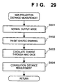
- Fig. 29 is a flow chart showing the operation of the non-projection distance measurement (second processing) executed in step S104 in Fig. 27.
- step S601 the output mode of the output signal OS in Fig. 5 is switched from the difference mode to the normal mode.
- step S602 the charge skimming operation is inhibited. That is, a charge in the cell 3 B is not cleared irrespective of the value of the signal SKOS.
- step S603 charges go around the ring CCDs 113b and 114b once to obtain image signals for one light projection from the sensor arrays 105 and 106 as output signals OS.
- step S604 the correlation of the image signals obtained by the two sensor arrays in step S603 is calculated, thereby obtaining a distance measurement value (correlation distance measurement). More specifically, the distance to the object to be measured is calculated using the principle of the trigonometric measurement on the basis of the relative values of the positions on the sensor arrays of the signals from the two sensor arrays.
- This step is executed in the same manner as in Fig. 28. Note that the reason why signal charges are caused to go around the CCDs once is to prevent generation of distance measurement errors due to an offset of image signals and to assure accurate distance measurements.
- step S505 in Fig. 28 and in step S604 in Fig. 29 will be explained below.
- A/D conversion is started in response to a signal SH to read out data for a round of the ring CCD 18. Furthermore, after corresponding signals in the cells 1 A and 2 A in the linear CCD 17 are cleared, a correlation calculation is performed to obtain the distance to the object to be measured.
- reflected light of light emitted by the light projecting portion is sensed, and when the amount of charges to be transferred to the CCD is smaller than the capacity of the skim element, the light projection of the IRED is stopped. Otherwise, an image signal is obtained using the IRED in the same manner as in the first embodiment.
- the distance to the object is measured on the basis of image data of the object obtained in this manner. For this reason, the distance can be accurately measured irrespective of an offset of the barycentric position of an image caused by the use of the IRED, and distance measurements can be prevented from being disabled due to perspective conflict, thus allowing accurate distance measurements.
- Fig. 30 shows a distance measuring device in which the device structure shown in Fig. 2 is partially modified, and a portion of the ring CCD 18 is not shown.
- Fig. 32 is a timing chart of this device.
- reference numeral 71 denotes OFF charge shift portions for shifting charges in the second accumulation portions (OFF charge accumulation portions) 14 to the linear CCD 17 in response to a pulse SH 2 .
- Reference numeral 72 denotes ON charge shift portions for shifting charges in the first accumulation portions (ON charge accumulation portions) 15 to the linear CCD 17 in response to a pulse SH 1 .
- a pulse IRED is kept at LOW level.
- the timing chart in Fig. 32 is different from that shown in Fig. 4 in that the pulse SH is divided into two pulses (SH 1 and SH 2 ).
- the pulse SH 2 is output at the same timing as the pulse SH in Fig. 4, and the pulse SH 1 is output at the timing of the next pulse CK.
- signal charges of a pair of adjacent sensor blocks can be added by the linear CCD 17. Therefore, a wrong distance measurement value can be prevented by the low-pass filter function from being obtained.
- signal charges from the sensor block S 2 are stored in the charge accumulation portions 14 and 15. Charges in the accumulation portion 14 are transferred to the cell 5 A in response to the pulse SH 2 . Charges in the cell 5 A are transferred to the cell 4 A in response to the next clock. At the same time, charges from the sensor block S 1 are added to those in the cell 4 A in response to the pulse SH 1 .
- the pulses SH 1 and SH 2 are generated at the same timings as those of the pulses SH, and the same operation as in Fig. 4 is performed.
- Fig. 33 is a view for explaining the method of amplifying an image signal on the device to emphasize its contrast in the non-projection distance measurement operation using the charge skimming function.
- curves indicated by "once”, “twice”, “four times”, and “eight times” respectively represent image signals of the accumulated charge amounts added by the ring CCDs 113b and 114b.
- the dynamic range must also be broadened accordingly. If the actual dynamic range is a range a, only signal charges for one light projection are not saturated, and signal charges added twice or more disturb a distance measurement operation. However, it is almost impossible to perform a distance measurement based on the correlation using a signal with such low contrast.
- charges are evenly skimmed by the skim portions 117 and 118 from image signals that are circulated through the CCDs 113b and 114b.
- a charge amount apparently in a range b can be output without being saturated, and only the range where the contrast of an image signal added twice is generated can be output as an image signal.
- Fig. 34 is a flow chart showing the non-projection distance measurement operation of the distance measuring device of this embodiment.
- step S111 the output mode of the output signal OS in Fig. 5 is switched to the normal mode.
- step S112 charge signals from the sensor arrays 105 and 106 are shifted to the charge transfer unit (ring CCDs 113b and 114b).
- step S113 it is checked by monitoring the outputs from the ring CCDs 113b and 114b if an image signal has a predetermined level or higher. If N in step S113, the flow advances to step S117; otherwise, the flow advances to step S114. Note that the predetermined level indicates a level corresponding to the amount of charges to be skimmed by one skimming operation of the skim portions 117 and 118. In step S117, charges from the sensor arrays 105 and 106 are shifted again to the charge transfer unit (ring CCDs 113b and 114b), and the flow advances to step S113.
- step S114 It is monitored in step S114 if the contrast is high enough to calculate the correlation of the image signals. If Y in step S114, the flow advances to step S115. In step S115, a correlation calculation is performed to obtain a distance measurement value.
- step S114 If it is determined in step S114 that the contrast is insufficient, the flow advances to step S116, and charges for one round of the ring CCDs 113b and 114b are unconditionally skimmed by the skim portions 117 and 118. Thereafter, the flow advances to step S117.
- the contrast can be emphasized, and distance measurements based on a correlation can be easily attained. Hence, even when the output from the sensor array has a low contrast, distance measurements can be performed.
- a light projecting portion may be arranged, and when the amount of charges to be removed by the skim portions 117 and 118 is larger than that from the sensor array, the processing shown in Fig. 34 may be selected and executed; otherwise, the processing shown in Fig. 28 may be executed. With this control, even when the luminance of external light is high, distance measurements can be reliably performed.
- the two different distance measurement methods i.e., the first processing executed in a state wherein the ON/OFF operation of the projected light spot is performed, and the second processing executed in a state wherein the projection of a light spot is turned off can be executed by a single device.
- the second processing signal charges are circulated through the ring portion while disabling the projection of a light spot and the operation of the skim portions, and the difference between signals from the two sensor arrays is not calculated. For this reason, distance measurements can be performed even for an object at a far distance or an object with a low reflectance from which a signal of the projected light spot is hardly obtained or when the luminance of external light is high.
Landscapes
- Engineering & Computer Science (AREA)
- Physics & Mathematics (AREA)
- Computer Networks & Wireless Communication (AREA)
- General Physics & Mathematics (AREA)
- Radar, Positioning & Navigation (AREA)
- Remote Sensing (AREA)
- Electromagnetism (AREA)
- Measurement Of Optical Distance (AREA)
- Focusing (AREA)
Applications Claiming Priority (6)
| Application Number | Priority Date | Filing Date | Title |
|---|---|---|---|
| JP26318295 | 1995-10-11 | ||
| JP263182/95 | 1995-10-11 | ||
| JP26318395A JPH09105624A (ja) | 1995-10-11 | 1995-10-11 | 測距装置 |
| JP26318295A JPH09105623A (ja) | 1995-10-11 | 1995-10-11 | 測距装置 |
| JP263183/95 | 1995-10-11 | ||
| JP26318395 | 1995-10-11 |
Publications (3)
| Publication Number | Publication Date |
|---|---|
| EP0768543A2 true EP0768543A2 (fr) | 1997-04-16 |
| EP0768543A3 EP0768543A3 (fr) | 1997-10-15 |
| EP0768543B1 EP0768543B1 (fr) | 2003-08-13 |
Family
ID=26545893
Family Applications (1)
| Application Number | Title | Priority Date | Filing Date |
|---|---|---|---|
| EP96307372A Expired - Lifetime EP0768543B1 (fr) | 1995-10-11 | 1996-10-10 | Télémètre |
Country Status (3)
| Country | Link |
|---|---|
| US (1) | US5850282A (fr) |
| EP (1) | EP0768543B1 (fr) |
| DE (1) | DE69629434T2 (fr) |
Cited By (3)
| Publication number | Priority date | Publication date | Assignee | Title |
|---|---|---|---|---|
| FR2784755A1 (fr) * | 1998-10-15 | 2000-04-21 | Asahi Optical Co Ltd | Appareil de mesure de distance |
| WO2002041031A1 (fr) * | 2000-11-14 | 2002-05-23 | Siemens Aktiengesellschaft | Dispositif de traitement de donnees image et procede y relatif |
| US6522393B2 (en) | 2000-05-01 | 2003-02-18 | Pentax Corporation | Distance measuring device |
Families Citing this family (7)
| Publication number | Priority date | Publication date | Assignee | Title |
|---|---|---|---|---|
| US6035138A (en) * | 1998-01-29 | 2000-03-07 | Canon Kabushiki Kaisha | Sensor apparatus applied to distance measuring apparatus, and method for controlling sensor apparatus |
| JPH11325886A (ja) * | 1998-05-08 | 1999-11-26 | Canon Inc | 測距装置及びコンピュータ読み取り可能な記憶媒体 |
| JP2000249906A (ja) * | 1999-02-26 | 2000-09-14 | Canon Inc | 撮像装置と測距装置 |
| EP1152261A1 (fr) * | 2000-04-28 | 2001-11-07 | CSEM Centre Suisse d'Electronique et de Microtechnique SA | Dispositif et procédé de détection avec résolution spatiale et démodulation d'ondes électromagnétiques modulées |
| JP2003066321A (ja) * | 2001-08-29 | 2003-03-05 | Mega Chips Corp | Af制御装置およびaf制御方法 |
| CN106775137B (zh) * | 2016-12-06 | 2019-10-25 | Oppo广东移动通信有限公司 | 接近检测方法、装置及移动终端 |
| US11518629B2 (en) * | 2019-10-28 | 2022-12-06 | Intelligrated Headquarters, Llc | Measurement system on a conveyor |
Citations (1)
| Publication number | Priority date | Publication date | Assignee | Title |
|---|---|---|---|---|
| JPH0522843A (ja) | 1991-07-09 | 1993-01-29 | Mitsubishi Electric Corp | 地絡方向継電装置 |
Family Cites Families (13)
| Publication number | Priority date | Publication date | Assignee | Title |
|---|---|---|---|---|
| US4373804A (en) * | 1979-04-30 | 1983-02-15 | Diffracto Ltd. | Method and apparatus for electro-optically determining the dimension, location and attitude of objects |
| JPS5810605A (ja) * | 1981-07-10 | 1983-01-21 | Canon Inc | 距離測定装置 |
| US4748469A (en) * | 1984-05-07 | 1988-05-31 | Canon Kabushiki Kaisha | Distance measuring device for camera |
| US4958180A (en) * | 1987-05-23 | 1990-09-18 | Minolta Camera Kabushiki Kaisha | Focus detecting device and auxiliary illuminating device therefor |
| DE3729334A1 (de) * | 1987-09-02 | 1989-03-16 | Sick Optik Elektronik Erwin | Lichttaster |
| US4943157A (en) * | 1989-05-18 | 1990-07-24 | Corning Incorporated | Fiber optic triangulation gage |
| US5293194A (en) * | 1990-01-25 | 1994-03-08 | Canon Kabushiki Kaisha | Focus detection apparatus having an auxiliary light |
| US5369462A (en) * | 1992-06-09 | 1994-11-29 | Olympus Optical Co., Ltd. | Inclination detecting apparatus and camera for detecting hand shake using the same |
| JP3406656B2 (ja) * | 1992-12-19 | 2003-05-12 | ペンタックス株式会社 | 測距装置 |
| JP3150243B2 (ja) * | 1993-10-25 | 2001-03-26 | キヤノン株式会社 | 測距装置及びカメラ |
| JP3406931B2 (ja) * | 1993-11-25 | 2003-05-19 | キヤノン株式会社 | Ccdの信号補正装置 |
| JP3359132B2 (ja) * | 1993-11-25 | 2002-12-24 | キヤノン株式会社 | 測距装置 |
| US5808726A (en) * | 1995-02-28 | 1998-09-15 | Canon Kabushiki Kaisha | Distance measurement apparatus |
-
1996
- 1996-10-08 US US08/727,376 patent/US5850282A/en not_active Expired - Fee Related
- 1996-10-10 EP EP96307372A patent/EP0768543B1/fr not_active Expired - Lifetime
- 1996-10-10 DE DE69629434T patent/DE69629434T2/de not_active Expired - Lifetime
Patent Citations (1)
| Publication number | Priority date | Publication date | Assignee | Title |
|---|---|---|---|---|
| JPH0522843A (ja) | 1991-07-09 | 1993-01-29 | Mitsubishi Electric Corp | 地絡方向継電装置 |
Cited By (6)
| Publication number | Priority date | Publication date | Assignee | Title |
|---|---|---|---|---|
| FR2784755A1 (fr) * | 1998-10-15 | 2000-04-21 | Asahi Optical Co Ltd | Appareil de mesure de distance |
| GB2344012A (en) * | 1998-10-15 | 2000-05-24 | Asahi Optical Co Ltd | Distance measuring apparatus |
| US6243537B1 (en) | 1998-10-15 | 2001-06-05 | Asahi Kogaku Kogyo Kabushiki Kaisha | Distance measuring apparatus |
| GB2344012B (en) * | 1998-10-15 | 2003-10-15 | Asahi Optical Co Ltd | Distance measuring apparatus |
| US6522393B2 (en) | 2000-05-01 | 2003-02-18 | Pentax Corporation | Distance measuring device |
| WO2002041031A1 (fr) * | 2000-11-14 | 2002-05-23 | Siemens Aktiengesellschaft | Dispositif de traitement de donnees image et procede y relatif |
Also Published As
| Publication number | Publication date |
|---|---|
| EP0768543B1 (fr) | 2003-08-13 |
| DE69629434T2 (de) | 2004-06-09 |
| DE69629434D1 (de) | 2003-09-18 |
| EP0768543A3 (fr) | 1997-10-15 |
| US5850282A (en) | 1998-12-15 |
Similar Documents
| Publication | Publication Date | Title |
|---|---|---|
| US6785469B1 (en) | Distance measuring device installed in camera | |
| WO1992009000A1 (fr) | Dispositif de detection de position focalisee | |
| US5850282A (en) | Distance measuring device | |
| US5808726A (en) | Distance measurement apparatus | |
| JPS62212611A (ja) | 自動焦点調節装置 | |
| US6647205B1 (en) | Distance-measuring sensor, distance-measuring device and camera as well as distance-measuring method | |
| JP3938989B2 (ja) | 測距装置 | |
| EP0933613A2 (fr) | Méthode et dispositif pour la mesure de distances | |
| US5892985A (en) | Eye ball detecting device | |
| JPH11153749A (ja) | 距離検出装置 | |
| JPS60176009A (ja) | 自動焦点カメラ | |
| US6104879A (en) | Signal forming apparatus | |
| JPH09105623A (ja) | 測距装置 | |
| JP2003015021A (ja) | 測距装置 | |
| JP3076054B2 (ja) | 光電変換装置 | |
| JPH09105624A (ja) | 測距装置 | |
| JP2004271291A (ja) | 測距装置 | |
| JPH09229673A (ja) | 測距装置 | |
| JP2002023045A (ja) | 測定装置及びカメラ | |
| JP3302328B2 (ja) | 合焦点検出装置 | |
| JPH09229677A (ja) | 測距装置 | |
| JPH08320223A (ja) | 測距装置 | |
| JP2004198888A (ja) | 撮像素子、測距装置及び撮影装置 | |
| JPH09222553A (ja) | 測距装置 | |
| JPH06324256A (ja) | パッシブ型オートフォーカス装置用測距装置 |
Legal Events
| Date | Code | Title | Description |
|---|---|---|---|
| PUAI | Public reference made under article 153(3) epc to a published international application that has entered the european phase |
Free format text: ORIGINAL CODE: 0009012 |
|
| AK | Designated contracting states |
Kind code of ref document: A2 Designated state(s): DE FR GB |
|
| PUAL | Search report despatched |
Free format text: ORIGINAL CODE: 0009013 |
|
| AK | Designated contracting states |
Kind code of ref document: A3 Designated state(s): DE FR GB |
|
| 17P | Request for examination filed |
Effective date: 19980225 |
|
| 17Q | First examination report despatched |
Effective date: 19990317 |
|
| GRAH | Despatch of communication of intention to grant a patent |
Free format text: ORIGINAL CODE: EPIDOS IGRA |
|
| GRAH | Despatch of communication of intention to grant a patent |
Free format text: ORIGINAL CODE: EPIDOS IGRA |
|
| GRAA | (expected) grant |
Free format text: ORIGINAL CODE: 0009210 |
|
| AK | Designated contracting states |
Designated state(s): DE FR GB |
|
| REG | Reference to a national code |
Ref country code: GB Ref legal event code: FG4D |
|
| REF | Corresponds to: |
Ref document number: 69629434 Country of ref document: DE Date of ref document: 20030918 Kind code of ref document: P |
|
| ET | Fr: translation filed | ||
| PLBE | No opposition filed within time limit |
Free format text: ORIGINAL CODE: 0009261 |
|
| STAA | Information on the status of an ep patent application or granted ep patent |
Free format text: STATUS: NO OPPOSITION FILED WITHIN TIME LIMIT |
|
| 26N | No opposition filed |
Effective date: 20040514 |
|
| PGFP | Annual fee paid to national office [announced via postgrant information from national office to epo] |
Ref country code: DE Payment date: 20091031 Year of fee payment: 14 |
|
| PGFP | Annual fee paid to national office [announced via postgrant information from national office to epo] |
Ref country code: GB Payment date: 20091028 Year of fee payment: 14 Ref country code: FR Payment date: 20091030 Year of fee payment: 14 |
|
| GBPC | Gb: european patent ceased through non-payment of renewal fee |
Effective date: 20101010 |
|
| PG25 | Lapsed in a contracting state [announced via postgrant information from national office to epo] |
Ref country code: FR Free format text: LAPSE BECAUSE OF NON-PAYMENT OF DUE FEES Effective date: 20101102 |
|
| REG | Reference to a national code |
Ref country code: FR Ref legal event code: ST Effective date: 20110630 |
|
| PG25 | Lapsed in a contracting state [announced via postgrant information from national office to epo] |
Ref country code: GB Free format text: LAPSE BECAUSE OF NON-PAYMENT OF DUE FEES Effective date: 20101010 |
|
| REG | Reference to a national code |
Ref country code: DE Ref legal event code: R119 Ref document number: 69629434 Country of ref document: DE Effective date: 20110502 |
|
| PG25 | Lapsed in a contracting state [announced via postgrant information from national office to epo] |
Ref country code: DE Free format text: LAPSE BECAUSE OF NON-PAYMENT OF DUE FEES Effective date: 20110502 |