EP0761599A2 - Verfahren zum Reinigen einer alkalischen Lösung und Methode zum Ätzen von Halbleiterscheiben - Google Patents
Verfahren zum Reinigen einer alkalischen Lösung und Methode zum Ätzen von Halbleiterscheiben Download PDFInfo
- Publication number
- EP0761599A2 EP0761599A2 EP96113770A EP96113770A EP0761599A2 EP 0761599 A2 EP0761599 A2 EP 0761599A2 EP 96113770 A EP96113770 A EP 96113770A EP 96113770 A EP96113770 A EP 96113770A EP 0761599 A2 EP0761599 A2 EP 0761599A2
- Authority
- EP
- European Patent Office
- Prior art keywords
- alkaline solution
- semiconductor wafers
- metallic
- purifying
- etching
- Prior art date
- Legal status (The legal status is an assumption and is not a legal conclusion. Google has not performed a legal analysis and makes no representation as to the accuracy of the status listed.)
- Granted
Links
Images





Classifications
-
- C—CHEMISTRY; METALLURGY
- C01—INORGANIC CHEMISTRY
- C01D—COMPOUNDS OF ALKALI METALS, i.e. LITHIUM, SODIUM, POTASSIUM, RUBIDIUM, CAESIUM, OR FRANCIUM
- C01D1/00—Oxides or hydroxides of sodium, potassium or alkali metals in general
- C01D1/04—Hydroxides
- C01D1/28—Purification; Separation
-
- H—ELECTRICITY
- H10—SEMICONDUCTOR DEVICES; ELECTRIC SOLID-STATE DEVICES NOT OTHERWISE PROVIDED FOR
- H10P—GENERIC PROCESSES OR APPARATUS FOR THE MANUFACTURE OR TREATMENT OF DEVICES COVERED BY CLASS H10
- H10P50/00—Etching of wafers, substrates or parts of devices
Definitions
- the present invention relates to a method of purifying an alkaline solution by effectively non-ionizing or removing metallic impurity ions therein and a method of etching semiconductor wafers which enables to etch them without deteriorating the quality thereof with an alkaline solution purified by using the purifying method.
- the manufacturing method of semiconductor wafers includes a slicing step to obtain wafers of thin disc shape by slicing a single crystal ingot formed by a pulling step using a crystal pulling machine; a chamfering step to chamfer a peripheral edge portion of the wafer obtained through the slicing step to prevent cracking or breakage of the wafer; a lapping step to flatten the surface of the chamfered wafer by lapping it; an etching step to remove processing damage of the so chamfered and lapped wafer; a polishing process to polish the surface of the etched wafer; and a cleaning step for cleaning the polished wafer to remove the polishing agent or dust particles from its surface.
- the etching step there are two types of steps, that is, an acid etching step using an acid etching solution of a mixed acid or the like and an alkaline etching step using an alkaline etching solution of NaOH or the like.
- the acid etching step the etching speed is fast and hence it is difficult to uniformly etch the wafer with a problem that flatness of the wafer is deteriorated. Therefore, recently an alkaline etching which uses a sodium hydroxide solution, a potassium hydroxide solution, and an alkyl ammonium hydroxide solution, etc. is predominantly employed because the alkaline etching does not deteriorate flatness of the wafer due to its uniform etching even if its etching speed is slow.
- an industrial alkaline solution on the market of high metallic impurity concentration is used as it is. It is needless to say that a lot of metallic impurities are included in the alkaline solution of the industrial grade generally used. Even an alkaline solution of the electronic industrial grade used for etching of the semiconductor wafer presently contains metallic impurities of several tens of ppb to several ppm.
- nickel, chromium, iron and copper as metallic impurities included in this alkaline solution.
- the present inventors keep researching the alkaline etching process during many years. According to a recent outcome of the present inventor's researches, in contradiction to the common sense of those skilled in the art, it was revealed the surprising fact that metallic ions of a part of metallic impurities such as copper and nickel which exist in the alkaline etching solution diffuse into the deep inside of the wafer while etching with the result that the wafer quality is deteriorated and the characteristic of the semiconductor device made of the wafer is remarkably degraded.
- an alkaline solution of high purity as measures to prevent deterioration in the wafer quality due to the alkaline etching solution.
- an alkaline solution of high purity on the market is only an extremely expensive alkaline solution of the analysis grade. It does not match at all in the cost to employ an alkaline solution for an analytical use as an industrial use.
- the inventors found by extended researches that metallic impurity ions in an alkaline solution are non-ionized by an easy technique and further semiconductor wafers etched with the alkaline solution in which metallic impurity ions were non-ionized or removed are not deteriorated even in the physical existence of the metallic impurities.
- the present invention was accomplished on the basis of the surprising finding.
- the present invention provides a method of purifying an alkaline solution which comprises the steps of dissolving metallic silicon and/or silicon compounds in an alkaline solution and non-ionizing metallic ions in the alkaline solution by reaction products such as hydrogen and silicates generated when the metallic silicon and/or silicon compounds are dissolved therein.
- metallic silicon there can be enumerated polysilicon and single crystal silicon. These can be used by mixing them or alone.
- silicon compounds silica and silicates can be enumerated and these can be used together or alone.
- metallic silicon and silicon compounds it is preferable to use products of as high purity as possible within the range commercially practicable.
- dissolution amount of the above-mentioned metallic silicon there is no special limitation for the dissolution amount of the above-mentioned metallic silicon as long as the effect of this invention is achieved, but 0.2 g/liter or more is suitable therefor. When the dissolution amount is too small, the achievement of the effect of this invention is not enough. When this dissolution amount is too large, it is disadvantageous from an economical viewpoint.
- the dissolution amount of the above-mentioned silicon compounds does not have a special limitation as long as the effect of this invention is achieved, but the dissolution amount of Si included in the dissolved silicon compound is suitably 5 g/liter or more.
- the dissolution amount is too small, the achievement of the effect of this invention is not enough.
- this dissolution amount is too large, it is disadvantageous from an economical viewpoint.
- the present invention provides a method of purifying an alkaline solution which comprises the steps of dissolving hydrogen gas in an alkaline solution and non-ionizing metallic ions in the alkaline solution by reducing them using the dissolved hydrogen gas.
- a method of etching semiconductor wafers which comprises the steps of purifying an alkaline solution by non-ionizing metallic ions in the alkaline solution and etching semiconductor wafers by using the purified alkaline solution.
- the purification processing of the alkaline solution may be conducted by previously described various modes of the method of purifying the alkaline solution.
- a method of etching semiconductor wafers which comprises the steps of removing metallic ions in an alkaline solution and etching semiconductor wafers by using the alkaline solution in which metallic ions have been removed.
- the removal processing of the metallic ions can be carried out with ion exchange resins, preferably chelate resins.
- ion exchange resins preferably chelate resins.
- alkaline solution used in this invention there may be given a sodium hydroxide solution or a potassium hydroxide solution conventionally and widely used as an alkaline etching solution of semiconductor wafers.
- nickel ions there are nickel ions, copper ions, chromium ions, iron ions, etc. as impurity metallic ions to be removed from the alkaline solution.
- impurity metallic ions it is important from a viewpoint of the semiconductor wafer quality to non-ionize or to remove the nickel ions and the copper ions with a large diffusion speed in silicon single crystal.
- a metallic ion concentration in an alkaline solution used in etching semiconductor wafers according to the present invention may be suitably limited to 50 ppb or less, preferably 20 ppb or less, more preferably 10 ppb or less. With these concentration limitations, the achievement of the effect of this invention is more enough.
- the purification of the alkaline solution of this invention connotes that impurity metallic ions in the alkaline solution are non-ionized or removed. Even if solid impurity metals exist physically in the alkaline solution, unless they exist in the state of metallic ions, the alkaline solution corresponds to the state of the purified alkaline solution according to this invention. That is, the quality deterioration of the semiconductor wafers due to the etching thereof does not occur even if solid impurity metals exist in an alkaline solution as long as they do not exist as impurity metallic ions. On the contrary, when the solid impurity metals do not exist at all but exist as metallic ions in the alkaline solution; if the semiconductor wafers are etched by using this alkaline solution, deterioration in the wafer quality thereof is caused.
- the present invention is based on three inventive findings: the first finding that the existence of impurity metallic ions in an alkaline solution greatly affects quality deterioration of semiconductor wafers due to alkaline etching; the second finding that purification such as non-ionization of the metallic ions in the alkaline solution can be carried out by a very easy technique; and the third finding that when semiconductor wafers are etched by using the purified alkaline solution quality deterioration thereof does not occur.
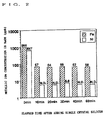
- Fig. 1 is a graph showing the relation between an iron ion concentration and a nickel ion concentration in the sodium hydroxide solution and the elapsed time after adding polysilicon thereto in Example 1.
- Fig. 2 is a graph showing the relation between an iron ion concentration and a nickel ion concentration in the sodium hydroxide solution and the elapsed time after adding single crystal silicon thereto in Example 2.
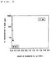
- Fig. 3 is a graph showing the relation between the amount of dissolved polysilicon and a nickel ion concentration in the sodium hydroxide solution in Example 3.
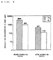
- Fig. 4 is a graph showing the relation between an iron ion concentration and a nickel ion concentration in the sodium hydroxide solution before and after dissolving silica in Example 4.
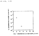
- Fig. 5 is a graph showing the relation between the amount of dissolved silicate and a nickel ion concentration in the sodium hydroxide solution in Example 5.
- Fig. 6 is a graph showing the relation between hydrogen gas blowing and an iron ion concentration and a nickel ion concentration in the sodium hydroxide solution in Example 6.
- Fig. 7 is a graph showing a nickel concentration on a wafer which was etched by a sodium hydroxide solution purified with polysilicon in Example 7 and that on another wafer which was etched by an unpurified sodium hydroxide solution.
- Fig. 8 is a graph showing a nickel concentration on a wafer which was etched by a sodium hydroxide solution purified with single crystal silicon in Example 8 and that on another wafer which was etched by an unpurified sodium hydroxide solution.
- Fig. 9 is a graph showing a nickel concentration on a wafer which was etched by a sodium hydroxide solution purified with silica in Example 9 and that on another wafer which was etched by an unpurified sodium hydroxide solution.
- Fig. 10 is a graph showing a nickel concentration on a wafer which was etched by a sodium hydroxide solution purified with silicate in Example 10 and that on another wafer which was etched by an unpurified sodium hydroxide solution.
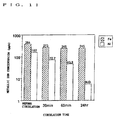
- Fig. 11 is a graph showing the relation between an iron ion concentration and a nickel ion concentration in the sodium hydroxide solution and the circulation time of the sodium hydroxide solution in Example 11 where the sodium hydroxide solution was highly purified with ion exchange resins.
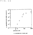
- Fig. 12 is a graph showing the relation between a nickel concentration on a wafer etched by a sodium hydroxide solution and a nickel ion concentration in the sodium hydroxide solution in Example 12.
- Fig. 13 is a graph showing the relation between a copper concentration on a wafer etched by a sodium hydroxide solution and a copper ion concentration in the sodium hydroxide solution in Example 12.
- Fig. 14 is a graph showing the relation between an iron concentration on a wafer etched by a sodium hydroxide solution and an iron ion concentration in the sodium hydroxide solution in Example 12.
- the wafer etched according to the above-mentioned condition was evaluated as follows. One side of the etched wafer was subjected to sand blasting and then thermal oxidation at 600°C. The thermal oxide film on the side of the wafer sand blasted was vapor phase decomposed with hydrofluoric acid vapor. The decomposed materials were collected by using a solution containing hydrofluoric acid. The collected materials were analyzed by ICP-MS (inductively coupled plasma mass spectrometer).
- Example 7 To a sodium hydroxide solution (45%, 20 liters and 80 °C), 200g of single crystal silicon (silicon wafer) was added. After leaving the solution for 60 minutes, a sample wafer was etched by using the solution under the condition same as Example 7 and the contamination level of the wafer was examined as Example 7.
- Example 7 To a sodium hydroxide solution (45%, 20 liters and 80 °C), 200g of silica was added. After leaving the solution for 60 minutes, a sample wafer was etched by using the solution under the condition same as Example 7 and the contamination level of the wafer was examined as Example 7.
- Example 7 Each sample wafer was etched by using the solution under the condition same as Example 7 and the contamination level of the wafer was examined as Example 7. The results of the examination indicated the fact that the nickel ion concentration on the wafer etched by this purified sodium hydroxide solution was remarkably decreased.
- the metallic ion concentration in the sodium hydroxide solution becomes 10 ppb or less, it is confirmed that the metal on the wafer hardly exists, too. In addition, it is also confirmed that metallic contamination on the wafer does not become so much if the metallic ion concentration in the sodium hydroxide solution is limited to 50 ppb or less. Further, it is confirmed that the metallic ion concentration therein is preferably 20 ppb or less and more preferably 10 ppb or less.
Landscapes
- Chemical & Material Sciences (AREA)
- Organic Chemistry (AREA)
- Engineering & Computer Science (AREA)
- Materials Engineering (AREA)
- Inorganic Chemistry (AREA)
- Weting (AREA)
- Cleaning Or Drying Semiconductors (AREA)
- Crystals, And After-Treatments Of Crystals (AREA)
Applications Claiming Priority (6)
| Application Number | Priority Date | Filing Date | Title |
|---|---|---|---|
| JP22035095 | 1995-08-29 | ||
| JP22035095 | 1995-08-29 | ||
| JP220350/95 | 1995-08-29 | ||
| JP218503/96 | 1996-08-20 | ||
| JP21850396A JP3678505B2 (ja) | 1995-08-29 | 1996-08-20 | 半導体ウェーハをエッチングするためのアルカリ溶液の純化方法及び半導体ウェーハのエッチング方法 |
| JP21850396 | 1996-08-20 |
Publications (3)
| Publication Number | Publication Date |
|---|---|
| EP0761599A2 true EP0761599A2 (de) | 1997-03-12 |
| EP0761599A3 EP0761599A3 (de) | 1999-01-07 |
| EP0761599B1 EP0761599B1 (de) | 2003-10-29 |
Family
ID=26522596
Family Applications (1)
| Application Number | Title | Priority Date | Filing Date |
|---|---|---|---|
| EP96113770A Expired - Lifetime EP0761599B1 (de) | 1995-08-29 | 1996-08-28 | Verfahren zum Reinigen einer alkalischen Lösung und Methode zum Ätzen von Halbleiterscheiben |
Country Status (6)
| Country | Link |
|---|---|
| US (1) | US6110839A (de) |
| EP (1) | EP0761599B1 (de) |
| JP (1) | JP3678505B2 (de) |
| KR (1) | KR100418443B1 (de) |
| DE (1) | DE69630496T2 (de) |
| MY (1) | MY119496A (de) |
Cited By (3)
| Publication number | Priority date | Publication date | Assignee | Title |
|---|---|---|---|---|
| EP0864533A3 (de) * | 1997-03-13 | 1999-04-07 | Shin-Etsu Handotai Company Limited | Verfahren zum Reinigen einer alkalischen Lösung und Methode zum Ätzen von Halbleiterscheiben |
| US6099748A (en) * | 1997-12-11 | 2000-08-08 | Shin-Etsu Handotai Co., Ltd. | Silicon wafer etching method and silicon wafer etchant |
| EP1168423A4 (de) * | 1999-12-28 | 2007-01-24 | Shinetsu Handotai Kk | Ätzlösung, ätzverfahren und halbleitersiliziumscheibe |
Families Citing this family (17)
| Publication number | Priority date | Publication date | Assignee | Title |
|---|---|---|---|---|
| US6074960A (en) * | 1997-08-20 | 2000-06-13 | Micron Technology, Inc. | Method and composition for selectively etching against cobalt silicide |
| KR20010064043A (ko) * | 1999-12-24 | 2001-07-09 | 구본준, 론 위라하디락사 | 박막트랜지스터 및 액정표시장치용 어레이기판제조방법 |
| US6503363B2 (en) | 2000-03-03 | 2003-01-07 | Seh America, Inc. | System for reducing wafer contamination using freshly, conditioned alkaline etching solution |
| WO2004027840A2 (en) * | 2002-09-18 | 2004-04-01 | Memc Electronic Materials, Inc. | Process for etching silicon wafers |
| JP4424039B2 (ja) | 2004-04-02 | 2010-03-03 | 株式会社Sumco | 半導体ウェーハの製造方法 |
| WO2006009668A1 (en) * | 2004-06-16 | 2006-01-26 | Memc Electronic Materials, Inc. | Silicon wafer etching process and composition |
| JP4487753B2 (ja) * | 2004-12-10 | 2010-06-23 | 株式会社Sumco | シリコンウェーハ用のアルカリエッチング液及び該エッチング液を用いたエッチング方法 |
| JP4517867B2 (ja) * | 2005-01-31 | 2010-08-04 | 株式会社Sumco | シリコンウェーハ表面形状制御用エッチング液及び該エッチング液を用いたシリコンウェーハの製造方法 |
| TW200745313A (en) * | 2006-05-26 | 2007-12-16 | Wako Pure Chem Ind Ltd | Substrate etching liquid |
| JP5142592B2 (ja) | 2007-06-06 | 2013-02-13 | 関東化学株式会社 | 基板の洗浄またはエッチングに用いられるアルカリ性水溶液組成物 |
| JP5040564B2 (ja) * | 2007-09-28 | 2012-10-03 | 株式会社Sumco | シリコンウェーハの製造方法 |
| WO2009107472A1 (ja) * | 2008-02-27 | 2009-09-03 | Jsr株式会社 | 化学機械研磨用水系分散体およびそれを用いた化学機械研磨方法、化学機械研磨用水系分散体の再生方法 |
| US8192822B2 (en) * | 2008-03-31 | 2012-06-05 | Memc Electronic Materials, Inc. | Edge etched silicon wafers |
| TW201006765A (en) * | 2008-08-07 | 2010-02-16 | Yeou Fa Chemical Co Ltd | Method for purifying potassium hydroxide aqueous solution rich in silicon impurities |
| CN102282647A (zh) * | 2008-11-19 | 2011-12-14 | Memc电子材料有限公司 | 剥除半导体晶片边缘的方法和系统 |
| US8853054B2 (en) | 2012-03-06 | 2014-10-07 | Sunedison Semiconductor Limited | Method of manufacturing silicon-on-insulator wafers |
| WO2026015399A1 (en) | 2024-07-10 | 2026-01-15 | Globalwafers Co., Ltd. | Etching apparatus that oscillate wafers during etching |
Family Cites Families (8)
| Publication number | Priority date | Publication date | Assignee | Title |
|---|---|---|---|---|
| JPS539295A (en) * | 1976-07-13 | 1978-01-27 | Nippon Soda Co Ltd | Production of high purity inorganic compounds |
| JPS5547221A (en) * | 1978-09-27 | 1980-04-03 | Tsurumi Soda Kk | Production of purified aqueous caustic alkali solution |
| JPS5574142A (en) * | 1978-11-28 | 1980-06-04 | Fuji Electric Co Ltd | Refining of semiconductor etching alkaline liquid |
| US4859280A (en) * | 1986-12-01 | 1989-08-22 | Harris Corporation | Method of etching silicon by enhancing silicon etching capability of alkali hydroxide through the addition of positive valence impurity ions |
| JP2994405B2 (ja) * | 1989-08-11 | 1999-12-27 | 関東化学株式会社 | 水酸化アルカリの精製法 |
| US5348617A (en) * | 1991-12-23 | 1994-09-20 | Iowa State University Research Foundation, Inc. | Selective etching process |
| JP3072876B2 (ja) * | 1993-09-17 | 2000-08-07 | 日曹エンジニアリング株式会社 | エッチング液の精製方法 |
| JP3075216B2 (ja) | 1997-06-11 | 2000-08-14 | 日本電気株式会社 | 交換機内部時計設定方式 |
-
1996
- 1996-08-20 JP JP21850396A patent/JP3678505B2/ja not_active Expired - Fee Related
- 1996-08-27 MY MYPI96003535A patent/MY119496A/en unknown
- 1996-08-27 US US08/703,645 patent/US6110839A/en not_active Expired - Lifetime
- 1996-08-28 DE DE69630496T patent/DE69630496T2/de not_active Expired - Lifetime
- 1996-08-28 EP EP96113770A patent/EP0761599B1/de not_active Expired - Lifetime
- 1996-08-29 KR KR1019960036304A patent/KR100418443B1/ko not_active Expired - Lifetime
Cited By (4)
| Publication number | Priority date | Publication date | Assignee | Title |
|---|---|---|---|---|
| EP0864533A3 (de) * | 1997-03-13 | 1999-04-07 | Shin-Etsu Handotai Company Limited | Verfahren zum Reinigen einer alkalischen Lösung und Methode zum Ätzen von Halbleiterscheiben |
| US6319845B1 (en) | 1997-03-13 | 2001-11-20 | Shin-Etsu Handotai Co., Ltd. | Method of purifying alkaline solution and method of etching semiconductor wafers |
| US6099748A (en) * | 1997-12-11 | 2000-08-08 | Shin-Etsu Handotai Co., Ltd. | Silicon wafer etching method and silicon wafer etchant |
| EP1168423A4 (de) * | 1999-12-28 | 2007-01-24 | Shinetsu Handotai Kk | Ätzlösung, ätzverfahren und halbleitersiliziumscheibe |
Also Published As
| Publication number | Publication date |
|---|---|
| DE69630496D1 (de) | 2003-12-04 |
| DE69630496T2 (de) | 2004-05-06 |
| KR970013092A (ko) | 1997-03-29 |
| US6110839A (en) | 2000-08-29 |
| MY119496A (en) | 2005-06-30 |
| JPH09129624A (ja) | 1997-05-16 |
| KR100418443B1 (ko) | 2004-06-30 |
| EP0761599A3 (de) | 1999-01-07 |
| EP0761599B1 (de) | 2003-10-29 |
| JP3678505B2 (ja) | 2005-08-03 |
Similar Documents
| Publication | Publication Date | Title |
|---|---|---|
| US6110839A (en) | Method of purifying alkaline solution and method of etching semiconductor wafers | |
| US7938982B2 (en) | Silicon wafer etching compositions | |
| US8298437B2 (en) | Alkali etching liquid for silicon wafer and etching method using same | |
| US20120080053A1 (en) | Method for cleaning of semiconductor substrate and acidic solution | |
| CN111936418B (zh) | 多晶硅破碎块及其制造方法 | |
| JP7018553B1 (ja) | 多結晶シリコン破砕塊及びその製造方法 | |
| US6319845B1 (en) | Method of purifying alkaline solution and method of etching semiconductor wafers | |
| JP2001077063A (ja) | シリコンウェーハの研磨液及びこれを用いた研磨方法 | |
| EP1168423A1 (de) | Ätzlösung, ätzverfahren und halbleitersiliziumscheibe | |
| JP2006324452A (ja) | 半導体基板表面処理剤及び処理方法 | |
| CN102054669B (zh) | 加工硅晶片的方法 | |
| JP2005347737A (ja) | シリコンウェハー用研磨組成物 | |
| US20090127501A1 (en) | Polishing Composition for Silicon Wafer | |
| US20080115423A1 (en) | Polishing Composition For Silicon Wafer | |
| JP2010027949A (ja) | シリコンウェーハ用エッチング液及びシリコンウェーハの製造方法 | |
| JP2000173956A (ja) | 半導体シリコンウェーハ研磨用研磨剤及び研磨方法 | |
| TW471062B (en) | Method of etching semiconductor wafers | |
| JP3400694B2 (ja) | シリコンウエハのエッチング方法 | |
| KR20100040598A (ko) | 실리콘 웨이퍼용 알칼리 에칭액 | |
| JP2003007672A (ja) | シリコン半導体ウェーハのエッチング方法 | |
| JP2005340649A (ja) | エッチング液、エッチング方法及び半導体ウェーハ | |
| JP2002353281A (ja) | シリコンウェーハ表面品質の評価方法 |
Legal Events
| Date | Code | Title | Description |
|---|---|---|---|
| PUAI | Public reference made under article 153(3) epc to a published international application that has entered the european phase |
Free format text: ORIGINAL CODE: 0009012 |
|
| AK | Designated contracting states |
Kind code of ref document: A2 Designated state(s): DE FR GB |
|
| PUAL | Search report despatched |
Free format text: ORIGINAL CODE: 0009013 |
|
| AK | Designated contracting states |
Kind code of ref document: A3 Designated state(s): DE FR GB |
|
| 17P | Request for examination filed |
Effective date: 19990618 |
|
| 17Q | First examination report despatched |
Effective date: 19990909 |
|
| GRAH | Despatch of communication of intention to grant a patent |
Free format text: ORIGINAL CODE: EPIDOS IGRA |
|
| GRAH | Despatch of communication of intention to grant a patent |
Free format text: ORIGINAL CODE: EPIDOS IGRA |
|
| GRAA | (expected) grant |
Free format text: ORIGINAL CODE: 0009210 |
|
| AK | Designated contracting states |
Kind code of ref document: B1 Designated state(s): DE FR GB |
|
| PG25 | Lapsed in a contracting state [announced via postgrant information from national office to epo] |
Ref country code: FR Free format text: LAPSE BECAUSE OF FAILURE TO SUBMIT A TRANSLATION OF THE DESCRIPTION OR TO PAY THE FEE WITHIN THE PRESCRIBED TIME-LIMIT Effective date: 20031029 |
|
| REG | Reference to a national code |
Ref country code: GB Ref legal event code: FG4D |
|
| REF | Corresponds to: |
Ref document number: 69630496 Country of ref document: DE Date of ref document: 20031204 Kind code of ref document: P |
|
| PG25 | Lapsed in a contracting state [announced via postgrant information from national office to epo] |
Ref country code: GB Free format text: LAPSE BECAUSE OF NON-PAYMENT OF DUE FEES Effective date: 20040828 |
|
| PLBE | No opposition filed within time limit |
Free format text: ORIGINAL CODE: 0009261 |
|
| 26N | No opposition filed |
Effective date: 20040730 |
|
| EN | Fr: translation not filed | ||
| GBPC | Gb: european patent ceased through non-payment of renewal fee |
Effective date: 20040828 |
|
| PGFP | Annual fee paid to national office [announced via postgrant information from national office to epo] |
Ref country code: DE Payment date: 20150825 Year of fee payment: 20 |
|
| REG | Reference to a national code |
Ref country code: DE Ref legal event code: R071 Ref document number: 69630496 Country of ref document: DE |