EP0741370B2 - Procédé pour appliquer un élément de sécurité sur un substrat - Google Patents
Procédé pour appliquer un élément de sécurité sur un substrat Download PDFInfo
- Publication number
- EP0741370B2 EP0741370B2 EP95810302A EP95810302A EP0741370B2 EP 0741370 B2 EP0741370 B2 EP 0741370B2 EP 95810302 A EP95810302 A EP 95810302A EP 95810302 A EP95810302 A EP 95810302A EP 0741370 B2 EP0741370 B2 EP 0741370B2
- Authority
- EP
- European Patent Office
- Prior art keywords
- substrate
- layer
- laminate
- adhesive layer
- security element
- Prior art date
- Legal status (The legal status is an assumption and is not a legal conclusion. Google has not performed a legal analysis and makes no representation as to the accuracy of the status listed.)
- Expired - Lifetime
Links
Images


Classifications
-
- B—PERFORMING OPERATIONS; TRANSPORTING
- B42—BOOKBINDING; ALBUMS; FILES; SPECIAL PRINTED MATTER
- B42D—BOOKS; BOOK COVERS; LOOSE LEAVES; PRINTED MATTER CHARACTERISED BY IDENTIFICATION OR SECURITY FEATURES; PRINTED MATTER OF SPECIAL FORMAT OR STYLE NOT OTHERWISE PROVIDED FOR; DEVICES FOR USE THEREWITH AND NOT OTHERWISE PROVIDED FOR; MOVABLE-STRIP WRITING OR READING APPARATUS
- B42D25/00—Information-bearing cards or sheet-like structures characterised by identification or security features; Manufacture thereof
- B42D25/40—Manufacture
- B42D25/45—Associating two or more layers
- B42D25/465—Associating two or more layers using chemicals or adhesives
- B42D25/47—Associating two or more layers using chemicals or adhesives using adhesives
-
- B—PERFORMING OPERATIONS; TRANSPORTING
- B42—BOOKBINDING; ALBUMS; FILES; SPECIAL PRINTED MATTER
- B42D—BOOKS; BOOK COVERS; LOOSE LEAVES; PRINTED MATTER CHARACTERISED BY IDENTIFICATION OR SECURITY FEATURES; PRINTED MATTER OF SPECIAL FORMAT OR STYLE NOT OTHERWISE PROVIDED FOR; DEVICES FOR USE THEREWITH AND NOT OTHERWISE PROVIDED FOR; MOVABLE-STRIP WRITING OR READING APPARATUS
- B42D25/00—Information-bearing cards or sheet-like structures characterised by identification or security features; Manufacture thereof
- B42D25/20—Information-bearing cards or sheet-like structures characterised by identification or security features; Manufacture thereof characterised by a particular use or purpose
- B42D25/29—Securities; Bank notes
-
- B—PERFORMING OPERATIONS; TRANSPORTING
- B42—BOOKBINDING; ALBUMS; FILES; SPECIAL PRINTED MATTER
- B42D—BOOKS; BOOK COVERS; LOOSE LEAVES; PRINTED MATTER CHARACTERISED BY IDENTIFICATION OR SECURITY FEATURES; PRINTED MATTER OF SPECIAL FORMAT OR STYLE NOT OTHERWISE PROVIDED FOR; DEVICES FOR USE THEREWITH AND NOT OTHERWISE PROVIDED FOR; MOVABLE-STRIP WRITING OR READING APPARATUS
- B42D25/00—Information-bearing cards or sheet-like structures characterised by identification or security features; Manufacture thereof
- B42D25/30—Identification or security features, e.g. for preventing forgery
- B42D25/328—Diffraction gratings; Holograms
-
- B—PERFORMING OPERATIONS; TRANSPORTING
- B42—BOOKBINDING; ALBUMS; FILES; SPECIAL PRINTED MATTER
- B42D—BOOKS; BOOK COVERS; LOOSE LEAVES; PRINTED MATTER CHARACTERISED BY IDENTIFICATION OR SECURITY FEATURES; PRINTED MATTER OF SPECIAL FORMAT OR STYLE NOT OTHERWISE PROVIDED FOR; DEVICES FOR USE THEREWITH AND NOT OTHERWISE PROVIDED FOR; MOVABLE-STRIP WRITING OR READING APPARATUS
- B42D25/00—Information-bearing cards or sheet-like structures characterised by identification or security features; Manufacture thereof
- B42D25/40—Manufacture
- B42D25/45—Associating two or more layers
- B42D25/455—Associating two or more layers using heat
-
- G—PHYSICS
- G06—COMPUTING; CALCULATING OR COUNTING
- G06K—GRAPHICAL DATA READING; PRESENTATION OF DATA; RECORD CARRIERS; HANDLING RECORD CARRIERS
- G06K19/00—Record carriers for use with machines and with at least a part designed to carry digital markings
- G06K19/06—Record carriers for use with machines and with at least a part designed to carry digital markings characterised by the kind of the digital marking, e.g. shape, nature, code
- G06K19/06009—Record carriers for use with machines and with at least a part designed to carry digital markings characterised by the kind of the digital marking, e.g. shape, nature, code with optically detectable marking
- G06K19/06046—Constructional details
-
- B42D2033/04—
-
- B42D2035/20—
Definitions
- EP 401 466 is a security element designed as a layered composite known for sticking on a document.
- the layer composite has diffraction structures that between a stabilization layer and a thermal activatable adhesive layer are embedded.
- the transfer of the layered group on the document, by the adhesive layer through the layer composite heat is supplied therethrough, the stabilization layer the heat evenly distributed and one locally excessive heating of the diffraction structures bearing layers of paint prevented.
- the layer composite serves because of its diffraction structures caused optical effects as a security element.
- hot stamping is the Application of a relatively high pressure and sufficient heating required what with security elements that have optical diffraction structure or interference effects, without impairing these security elements not without further is possible.
- the lacquer layer 3 can also directly be applied to the backing layer 1 if the adhesiveness the lacquer layer 3 on the carrier layer 1 is sufficient.
- Adhesion can advantageously be by means of a Pretreatment of the carrier layer 1, e.g. B. in a corona or plasma discharge. A boundary layer between the lacquer layer 3 and the carrier layer 1 or one modified by the pretreatment Surface layer of the film takes over in these examples the function of the intermediate layer 2.
- the lacquer layer 3 can be applied directly be applied to the backing layer 1 if the adhesiveness the lacquer layer 3 on the carrier layer 1 so is agreed that after connecting the layer composite 7 with the substrate 9 on the carrier layer 1 those points of the layer composite 7 that on adhere to the substrate 9, easily from the paint layer 3 can be separated and that the carrier layer 1 at those points in the layer composite 7 that are not adhere to the substrate 9, the layers 3, 4, 5, 6 of the Layer composite 7 pulls, the layers 3, 4, 5, 6 along the border between the adhesive and the non-adhesive areas of the layer composite 7 tear.
- the first lacquer layer 3 is advantageous in at least applied in one operation and typically has one Layer thickness between 0.5 and 3.0 micrometers, preferably 1.5 microns.
- the relief of the diffraction structures 8 has a typical one Profile height that ranges from about 0.1 to 1.5 microns, while the grid spacing of the Diffraction structures 8 is about 0.1 to 10 microns.
- An application of the second lacquer layer 5 of about 0.15 to 1.5 micron thickness (e.g. 1 micron) levels the relief completely. It is advantageous for both layers of paint 3 and 5 uses the same material, for example a thermoplastic acrylic polymer paint.
- the second lacquer layer 5 serves primarily as an adhesion promoter between the reflective layer 4 and the adhesive layer 6. If necessary, they can be dispensed with become.
- the acrylic polymer lacquer of the lacquer layer 3 can do so be colored such that they are at least in a predetermined Part of the light spectrum is transparent.
- the Diffraction structure 8 remains in a predetermined wavelength range can be read out mechanically or visually. Is for example the dye for infrared light only permeable, the diffraction structure 8 is the unarmed Eye hidden and only by means of one not here shown reader recognizable that the presence the diffraction structure 8 is able to determine.
- the finished layer composite 7 leaves the Rewinding system, for example in the form of a roll, the graphic compositions from diffraction structures 8 which optical effects of the above Kind of effect.
- the detection system 14 can also be set up for this be the exact location of on the laminate 7 existing partial areas with diffraction structures Represent 8 provided elements to determine so that selected, well-defined elements of the layer composite 7 can be transferred to the substrate 9 are.
- the positioning is preferably carried out in y direction by shifting a single roll of the Rewinding system, because the inertia of the film tape is very is low.
- the shift of a single role is enough because with correct basic setting of the system only small displacements are necessary that the foil tape don't warp.
- the adhesive layer After the adhesive layer has cooled 6 will be the carrier film in a next step 1, 2 subtracted.
- the intermediate layer comes off 2 of the lacquer layer 3 at those points of the layer composite 7, which has previously been sufficiently heated were and thus adhere to the substrate 9.
- the intermediate layer 2 On the non-adhesive areas of the adhesive layer on the substrate 9 6, the intermediate layer 2 does not separate the lacquer layer 3 and the layers 3, 4, 5, 6 tear along the border between the sticky and the non-adhesive areas so that layers 3, 4, 5, 6 at the adhesive points of the layer composite 7 the substrate 9 remain.
- the use of the guided laser beam 12 enables further an application of the Layer composite 7 on the substrate 9 in two ways.
- the detection system 14 (Fig. 2) the location of, for example, on the Substrate 9 printed patterns with high accuracy to determine and then the laser beam 12 according to the location of these patterns that after peeling off the backing sheet on the substrate 9 remaining parts of the layer composite 7 in register to which patterns are aligned.
- a guilloche on a document to apply, of which individual lines are printed and individual Lines as layer composite 7 with diffraction structures 8 are glued on.
- Another option is there in it, parts of a graphic element, a character or a number, etc. with printing ink and the the element, the character or the Additional parts in register in the form of a transferred layer composite 7 with diffraction structures 8 to train.
- This combination of different Technologies result in a high level of security against Counterfeiting and manipulation.
- a security element it is possible as a security element to provide a layered composite 7 which is a predetermined one Design of elements such as Lines, pixels, Points, surface elements, etc., the special Diffraction structures 8 contained in their interaction for example create an optical effect, as from products sold under the brand name KINEGRAM® are sold, are known.
- the detection system 14 is now, as described above, set up to recognize the location of this design so the laser beam 12 is exactly over the elements of this design can be done. After peeling off the carrier film then this design remains on the Substrate 9 back. With this technology you can on the one hand, fine details such as very narrow lines the layer composite 7 transferred to the substrate 9.
- Reflective layer 4 there is a layer composite 7 with a highly reflective one Reflective layer 4 can be used, which is a high brilliance of the transmitted diffraction structures 8 guaranteed.
- an optical security element like a KINEGRAM® occupied area with diffraction structures 8 provided.
- the rest of the surface is optically diffraction not active and can in particular like a mirror Act.
- the substrate 9 is also within the assigned to the optical security element Area only partially covered. Thanks to the strong reflective reflection layer 4 appears the diffraction optical Security element nevertheless in high Brilliance.
- the method with the controlled laser beam 12 is particularly suitable for accurate application a security element to counterfeiting protective document, such as a banknote.
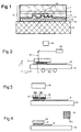
- the 8 and 9 show in plan view and in cross section a banknote 37 with patterns 38 and with a continuous Number 39 is printed and a security element 40, which represents the same number 39.
- the banknote has lines 41 which are made of Sub-lines 42 and 43 of a first and a second type are composed.
- the sub-lines 42 and 43 are in 8 drawn or drawn in dashed lines.
- the control device detects by means of of the detection system 14 the exact xy position of the Banknote 37 and the value of number 39.
- the security element 40 is made from a layer composite 7 (Fig.
- a locally limited or a full area for visible Transparent protective layer 44 e.g. from a UV curable varnish to apply to the diffractive Line elements of number 40 and lines 41 protect against mechanical abrasion.
Claims (11)
- Procédé à appliquer un élément de sécurité (25; 26; 27; 28) sur un substrat (9), dans lequel l'élément de sécurité (25; 26; 27; 28) est configuré comme un composite multicouche (7) qui comprend au moins un film support (1; 1, 2) et une couche d'adhésif ((6) apte à être activée de manière thermique pour la liaison avec ledit substrat (9) et qui comprend des structures (8) de diffraction optique et/ou un paquet stratifié (45) à couches produisant des effets d'interférence, dans lequel ladite couche d'adhésif (6) est mise en contact avec ledit substrat (9) et chauffée à travers ledit composite multicouche (7) de façon, que ledit composite multicouche (7) adhère sur ledit substrat (9) au niveau des endroits chauffés, sans que lesdites structures de diffraction (8) ou respectivement ledit paquet stratifié (45) soient détruits,
caractérisé en ce que ladite couche d'adhésif (6) n'est chauffée, par amenée de l'énergie rayonnante sous forme de rayons laser (12), que localement sous forme d'un motif à lignes à une largeur de ligne entre quelques micromètres et quelques dizaines de micromètres, par exemple 60 µm, ou en tant qu'un élément plan aux dimensions entre 10 et 100 micromètres. - Procédé à appliquer un élément de sécurité (25; 26; 27; 28) sur un substrat (9), dans lequel l'élément de sécurité (25; 26; 27; 28) est configuré comme un composite multicouche (7) qui comprend au moins un film support (1; 1, 2) et une couche d'adhésif ((6) apte à être activée de manière thermique pour la liaison avec ledit substrat (9) et qui comprend des structures (8) de diffraction optique et/ou un paquet stratifié (45) à couches produisant des effets d'interférence, dans lequel ladite couche d'adhésif (6) est mise en contact avec ledit substrat (9) et chauffée à travers ledit composite multicouche (7) de façon, que ledit composite multicouche (7) adhère sur ledit substrat (9) au niveau des endroits chauffés, sans que lesdites structures de diffraction (8) ou respectivement ledit paquet stratifié (45) soient détruits,
caractérisé en ce que ladite couche d'adhésif (6) n'est chauffée que localement par amenée de l'énergie rayonnante sous forme d'exposition à un système (19) adressable constitué de diodes laser ou de diodes lumineuses. - Procédé à appliquer un élément de sécurité (25; 26; 27; 28) sur un substrat (9), dans lequel l'élément de sécurité (25; 26; 27; 28) est configuré comme un composite multicouche (7) qui comprend au moins un film support (1; 1, 2) et une couche d'adhésif ((6) apte à être activée de manière thermique pour la liaison avec ledit substrat (9) et qui comprend des structures (8) de diffraction optique et/ou un paquet stratifié (45) à couches produisant des effets d'interférence, dans lequel ladite couche d'adhésif (6) est mise en contact avec ledit substrat (9) et chauffée à travers ledit composite multicouche (7) de façon, que ledit composite multicouche (7) adhère sur ledit substrat (9) au niveau des endroits chauffés, sans que lesdites structures de diffraction (8) ou respectivement ledit paquet stratifié (45) soient détruits,
caractérisé en ce que ladite couche d'adhésif (6) n'est chauffée, par amenée de l'énergie rayonnante à travers un masque (17) ou au moyen d'un modulateur de lumière tridimensionnelle, qui comprend une matrice à éléments d'image adressables, que localement en un grand nombre de surfaces partielles dudit composite multicouche (7) en même temps. - Procédé selon une quelconque des revendications précédentes,
caractérisé en ce que ledit film support (1; 1, 2) est décalqué, après collage de ladite couche d'adhésif (6) sur ledit substrat (9), ledit film support (1; 1, 2) se détachant des autres couches (3, 4, 5, 6; 45, 46, 6) dudit composite multicouche (7) au niveau des endroits adhérant sur ledit substrat (9), et lesdites couches (3, 4, 5, 6; 45, 46, 6) se déchirant le long de la limite entre les endroits adhérant et les endroits non adhérant, de sorte que ces couches (3, 4, 5, 6; 45, 46, 6) ne restent sur ledit substrat (9) qu'au niveau des endroits adhérent. - Procédé selon les revendications 1 et 4,
caractérisé en ce que la position xy dudit substrat (9) est détectée au moyen d'un système de reconnaissance (14), et en ce que la position dudit rayon laser (12) est alignée sur la position xy dudit composite multicouche (7) lors de l'application dudit composite multicouche (7). - Procédé selon les revendications 1 et 4,
caractérisé en ce que ledit composite multicouche (7) comprend des surfaces partielles dotées de structures de diffraction (8), en ce que la position xy dudit composite multicouche (7) est détectée au moyen d'un système de reconnaissance (14), et en ce que la position dudit rayon laser (12) est alignée sur la position xy dudit composite multicouche (7) lors de l'application dudit composite multicouche (7). - Procédé selon les revendications 1, 5 et 6,
caractérisé en ce que la position xy dudit substrat (9) et la position xy dudit composite multicouche (7) sont alignées l'une sur l'autre au moyen d'un système de positionnement (50). - Procédé selon une quelconque des revendications 4 à 7,
caractérisé en ce que ledit substrat (9) est recouvert d'une couche de protection (44) pour la protection des couches localement restées (3, 4, 5, 6; 45, 46, 6) dudit composite multicouche (7) contre l'usure mécanique par frottement ou contre toute modification. - Procédé selon une quelconque des revendications 4 à 8,
caractérisé en ce que l'élément de sécurité (27) comprend des caractères, en particulier des chiffres, et en ce que l'aire occupée par un seul caractère contient de nombreux petits caractères de la même nature. - Procédé selon une quelconque des revendications 4 à 9,
caractérisé en ce que ledit substrat (9) est un document, en particulier un billet de banque, qui contient des motifs ou des caractères, en particulier des chiffres, qui sont composés de lignes partielles (42, 43) d'un premier type et d'un deuxième type, lesdites lignes partielles (42) dudit premier type étant composée d'encre d'imprimerie et lesdites lignes partielles (43) dudit deuxième type étant configurée aux structures de diffraction (8) ou aux couches (45) produisant des effets d'interférence, et en ce que lesdites lignes partielles (42, 43) dudit premier type et dudit deuxième type sont alignées l'une sur l'autre à une précision de repérage point sur point. - Procédé selon une quelconque des revendications 4 à 10 pour un substrat (9), qui est un chèque (33) ou un titre, dont la valeur est fixée par l'indication d'une somme d'argent (36),
caractérisé en ce que les chiffres représentant ladite somme d'argent (36) sont transfert comme élément de sécurité (27).
Priority Applications (7)
| Application Number | Priority Date | Filing Date | Title |
|---|---|---|---|
| EP95810302A EP0741370B2 (fr) | 1995-05-05 | 1995-05-05 | Procédé pour appliquer un élément de sécurité sur un substrat |
| ES95810302T ES2120704T5 (es) | 1995-05-05 | 1995-05-05 | Procedimiento para aplicar un elemento de seguridad sobre un substrato. |
| DE59503265T DE59503265D1 (de) | 1995-05-05 | 1995-05-05 | Verfahren zum Aufbringen eines Sicherheitselementes auf ein Substrat |
| AT95810302T ATE170014T1 (de) | 1995-05-05 | 1995-05-05 | Verfahren zum aufbringen eines sicherheitselementes auf ein substrat |
| US08/614,513 US5882463A (en) | 1995-05-05 | 1996-03-13 | Method of applying a security element to a substrate |
| JP8058607A JPH08300801A (ja) | 1995-05-05 | 1996-03-15 | 機密保護要素を基層上に転写する方法と機密保護要素を有する書類 |
| RU96108966A RU2149763C1 (ru) | 1995-05-05 | 1996-05-05 | Способ нанесения защитного элемента на основу |
Applications Claiming Priority (1)
| Application Number | Priority Date | Filing Date | Title |
|---|---|---|---|
| EP95810302A EP0741370B2 (fr) | 1995-05-05 | 1995-05-05 | Procédé pour appliquer un élément de sécurité sur un substrat |
Publications (3)
| Publication Number | Publication Date |
|---|---|
| EP0741370A1 EP0741370A1 (fr) | 1996-11-06 |
| EP0741370B1 EP0741370B1 (fr) | 1998-08-19 |
| EP0741370B2 true EP0741370B2 (fr) | 2001-11-14 |
Family
ID=8221739
Family Applications (1)
| Application Number | Title | Priority Date | Filing Date |
|---|---|---|---|
| EP95810302A Expired - Lifetime EP0741370B2 (fr) | 1995-05-05 | 1995-05-05 | Procédé pour appliquer un élément de sécurité sur un substrat |
Country Status (7)
| Country | Link |
|---|---|
| US (1) | US5882463A (fr) |
| EP (1) | EP0741370B2 (fr) |
| JP (1) | JPH08300801A (fr) |
| AT (1) | ATE170014T1 (fr) |
| DE (1) | DE59503265D1 (fr) |
| ES (1) | ES2120704T5 (fr) |
| RU (1) | RU2149763C1 (fr) |
Cited By (13)
| Publication number | Priority date | Publication date | Assignee | Title |
|---|---|---|---|---|
| US7667895B2 (en) | 1999-07-08 | 2010-02-23 | Jds Uniphase Corporation | Patterned structures with optically variable effects |
| US7674501B2 (en) | 2002-09-13 | 2010-03-09 | Jds Uniphase Corporation | Two-step method of coating an article for security printing by application of electric or magnetic field |
| US7876481B2 (en) | 1999-07-08 | 2011-01-25 | Jds Uniphase Corporation | Patterned optical structures with enhanced security feature |
| US7934451B2 (en) | 2002-07-15 | 2011-05-03 | Jds Uniphase Corporation | Apparatus for orienting magnetic flakes |
| US8025952B2 (en) | 2002-09-13 | 2011-09-27 | Jds Uniphase Corporation | Printed magnetic ink overt security image |
| US8118963B2 (en) | 2002-09-13 | 2012-02-21 | Alberto Argoitia | Stamping a coating of cured field aligned special effect flakes and image formed thereby |
| US8343615B2 (en) | 2002-07-15 | 2013-01-01 | Jds Uniphase Corporation | Dynamic appearance-changing optical devices (DACOD) printed in a shaped magnetic field including printable fresnel structures |
| US8658280B2 (en) | 2002-09-13 | 2014-02-25 | Jds Uniphase Corporation | Taggent flakes for covert security applications having a selected shape |
| US9102195B2 (en) | 2012-01-12 | 2015-08-11 | Jds Uniphase Corporation | Article with curved patterns formed of aligned pigment flakes |
| US9164575B2 (en) | 2002-09-13 | 2015-10-20 | Jds Uniphase Corporation | Provision of frames or borders around pigment flakes for covert security applications |
| US9458324B2 (en) | 2002-09-13 | 2016-10-04 | Viava Solutions Inc. | Flakes with undulate borders and method of forming thereof |
| US9522402B2 (en) | 2002-07-15 | 2016-12-20 | Viavi Solutions Inc. | Method and apparatus for orienting magnetic flakes |
| WO2018197531A1 (fr) | 2017-04-28 | 2018-11-01 | Schmid Rhyner Ag | Dispositif et procédé permettant de produire un revêtement texturé |
Families Citing this family (68)
| Publication number | Priority date | Publication date | Assignee | Title |
|---|---|---|---|---|
| GB9510430D0 (en) * | 1995-05-22 | 1995-07-19 | Molins Plc | Printing method and apparatus |
| US6372073B1 (en) * | 1999-08-11 | 2002-04-16 | Southpac Trust International Inc. | Process for producing holographic material |
| US20040007315A1 (en) * | 1995-06-07 | 2004-01-15 | Weder Donald E. | Process for producing holographic material |
| DE19529171A1 (de) * | 1995-08-08 | 1997-02-13 | Giesecke & Devrient Gmbh | Transferband |
| DE19819571A1 (de) | 1998-04-30 | 1999-11-04 | Giesecke & Devrient Gmbh | Wertdokument mit Sicherheitselement |
| JP4311506B2 (ja) * | 1998-06-04 | 2009-08-12 | コニカミノルタエムジー株式会社 | Ic冊子 |
| US20040113420A1 (en) * | 2002-12-16 | 2004-06-17 | Wenyu Han | Cards with enhanced security features and associated apparatus and methods |
| DE19907697A1 (de) * | 1999-02-23 | 2000-08-24 | Giesecke & Devrient Gmbh | Wertdokument |
| DE19921579C2 (de) * | 1999-05-10 | 2002-02-07 | Kurz Leonhard Fa | Verfahren zur bereichsweisen Übertragung der Dekorlage einer Transferfolie auf ein Substrat sowie hierfür geeignete Transferfolie |
| US6761959B1 (en) | 1999-07-08 | 2004-07-13 | Flex Products, Inc. | Diffractive surfaces with color shifting backgrounds |
| US20030029082A1 (en) * | 1999-08-11 | 2003-02-13 | Weder Donald E. | Wrapper having a holographic image thereon |
| US6432244B1 (en) * | 1999-08-11 | 2002-08-13 | Southpac Trust Incorporated | Process for producing holographic material |
| US6444072B1 (en) * | 1999-08-11 | 2002-09-03 | Southpac Trust International | Process for producing holographic material |
| US20030000630A1 (en) * | 1999-08-11 | 2003-01-02 | Weder Donald E. | Method for forming a decorative cover having a holographic image thereon |
| US20020195192A1 (en) * | 1999-08-11 | 2002-12-26 | Weder Donald E. | Method for forming a wrapper having a holographic image thereon |
| US20030010428A1 (en) * | 1999-08-11 | 2003-01-16 | Weder Donald E. | Method for forming a decorative cover having a holographic image thereon |
| US20030104179A1 (en) * | 1999-08-11 | 2003-06-05 | Weder Donald E. | Holographic material |
| US6454895B1 (en) * | 1999-08-11 | 2002-09-24 | Southpac Trust International, Inc. | Process for producing holographic material |
| ATE424589T1 (de) * | 1999-08-12 | 2009-03-15 | Ovd Kinegram Ag | Datenträger |
| US11768321B2 (en) | 2000-01-21 | 2023-09-26 | Viavi Solutions Inc. | Optically variable security devices |
| DE10007916A1 (de) * | 2000-02-21 | 2001-08-23 | Giesecke & Devrient Gmbh | Mehrschichtige, laminierte Karte mit eingelagertem, Reliefstrukturen aufweisenden Sicherheitselement |
| DE10008851A1 (de) † | 2000-02-25 | 2001-08-30 | Giesecke & Devrient Gmbh | Verfahren zur Herstellung laserbeschriftbarer Datenträger und damit hergestellte Datenträger |
| TW515722B (en) * | 2000-05-03 | 2003-01-01 | Novo Nordisk As | Coding of cartridges for an injection device, a reading head and a reading system for reading code |
| US6533183B2 (en) | 2000-05-03 | 2003-03-18 | Novo Nordisk A/S | Coding of cartridges for an injection device |
| US6994261B2 (en) * | 2000-08-10 | 2006-02-07 | Novo Nirdisk A/S | Support for a cartridge for transferring an electronically readable item of information from the cartridge to an electronic circuit |
| EP1309366B1 (fr) * | 2000-08-10 | 2007-02-21 | Novo Nordisk A/S | Dispositif d'administration de medicament avec un support destine a une cartouche |
| DE10139719A1 (de) | 2000-11-04 | 2002-05-08 | Kurz Leonhard Fa | Mehrschichtkörper, insbesondere Mehrschichtenfolie sowie Verfahren zur Erhöhung der Fälschungssicherheit eines Mehrschichtenkörpers |
| DE50102764D1 (de) | 2000-11-04 | 2004-08-05 | Kurz Leonhard Fa | Kunststoffkörper als folie, z.b. transferfolie oder laminierfolie ausgebildet oder mit einer solchen folie versehen sowie verfahren zur herstellung eines mehrfarbenbildes auf oder in einem solchen kunststoffkörper |
| US20060162840A1 (en) * | 2000-12-05 | 2006-07-27 | Fryco Limited | Method of forming substrates wih visual features |
| US6493014B2 (en) * | 2000-12-22 | 2002-12-10 | Impress Systems | Optical security device printing system |
| DE10150194B4 (de) * | 2001-10-12 | 2013-08-22 | Morpho Cards Gmbh | Chipkarte |
| US6943952B2 (en) * | 2002-04-08 | 2005-09-13 | Hologram Industries (Sa) | Optical security component |
| FR2838202B1 (fr) * | 2002-04-08 | 2004-10-22 | Hologram Ind | Composant optique de securite |
| FR2838201B1 (fr) * | 2002-04-08 | 2004-07-16 | Hologram Ind Sarl | Composant optique de securite |
| US6580054B1 (en) * | 2002-06-10 | 2003-06-17 | New Wave Research | Scribing sapphire substrates with a solid state UV laser |
| US11230127B2 (en) | 2002-07-15 | 2022-01-25 | Viavi Solutions Inc. | Method and apparatus for orienting magnetic flakes |
| EP1608305B1 (fr) | 2003-03-24 | 2008-07-30 | Novo Nordisk A/S | Marquage electronique transparent de réservoir de medicaments |
| US6816180B1 (en) * | 2003-05-05 | 2004-11-09 | Eastman Kodak Company | Authenticated images on labels |
| US7544266B2 (en) * | 2004-05-21 | 2009-06-09 | Illinois Tool Works Inc. | Process of making laminated sheet and product made by the process |
| GB0416862D0 (en) * | 2004-07-29 | 2004-09-01 | Hewlett Packard Development Co | Products with data-encoding pattern |
| DE102004045211B4 (de) | 2004-09-17 | 2015-07-09 | Ovd Kinegram Ag | Sicherheitsdokument mit elektrisch gesteuertem Anzeigenelement |
| US7691281B2 (en) * | 2005-04-28 | 2010-04-06 | Harmony Fastening Systems, Inc. | Method of producing a reflective design |
| ATE495775T1 (de) | 2005-05-10 | 2011-02-15 | Novo Nordisk As | Injektionsvorrichtung mit optischem sensor |
| EA008115B1 (ru) * | 2005-06-13 | 2007-04-27 | Шамрило, Валерий Михайлович | Многослойный материал для изготовления самоклеящихся защитных меток (вариант) и способ его изготовления |
| GB2429187B (en) | 2005-08-15 | 2007-08-08 | Rue De Int Ltd | Security devices for security substrates |
| JP2007076069A (ja) * | 2005-09-12 | 2007-03-29 | Fujifilm Corp | ディスプレイ用光学シートの製造方法 |
| RU2432549C2 (ru) * | 2005-09-22 | 2011-10-27 | Ново Нордиск А/С | Способ и прибор для бесконтактного определения абсолютного положения и устройство, снабженное данным прибором |
| GB0524560D0 (en) * | 2005-12-01 | 2006-01-11 | Optaglio Ltd | Optical security device |
| JP2007193387A (ja) * | 2006-01-17 | 2007-08-02 | Dainippon Printing Co Ltd | セキュリティ情報媒体読取装置 |
| JP2009530001A (ja) * | 2006-03-20 | 2009-08-27 | ノボ・ノルデイスク・エー/エス | カートリッジの識別コードの非接触読取り |
| US8994382B2 (en) | 2006-04-12 | 2015-03-31 | Novo Nordisk A/S | Absolute position determination of movably mounted member in medication delivery device |
| JP2009534147A (ja) | 2006-04-26 | 2009-09-24 | ノボ・ノルデイスク・エー/エス | 薬剤送達装置における運動エレメントの非接触式の絶対位置測定 |
| FR2904723B1 (fr) * | 2006-08-01 | 2008-12-19 | Arjowiggins Security Soc Par A | Structure de securite, notamment pour un document de securite et/ou de valeur |
| US20080258457A1 (en) * | 2006-09-08 | 2008-10-23 | De La Rue International Limited | Method of manufacturing a security device |
| CN101641127B (zh) * | 2007-03-21 | 2012-11-28 | 诺沃-诺迪斯克有限公司 | 具有容器识别的医药输送系统和用于医药输送系统的容器 |
| EP1998550A1 (fr) * | 2007-05-24 | 2008-12-03 | Constantia Hueck Folien GmbH & Co. KG | Caractéristique de sécurité morphologique |
| JP2010528793A (ja) * | 2007-06-09 | 2010-08-26 | ノボ・ノルデイスク・エー/エス | リザーバ識別コードの無接触読み取り機能を有する装置 |
| DE102007036838A1 (de) * | 2007-08-02 | 2009-02-05 | Bundesdruckerei Gmbh | Verfahren zum Verbinden von Dokumentmaterialien unterschiedlichen Typs in einem Mehrschichtsicherheitsdokumentkörper |
| DE102008013167A1 (de) * | 2008-03-07 | 2009-09-10 | Giesecke & Devrient Gmbh | Sicherheitselement und Verfahren zu seiner Herstellung |
| US20100086753A1 (en) * | 2008-10-02 | 2010-04-08 | Wade Johnson | Foiled articles and methods of making same |
| CA2738880A1 (fr) | 2008-11-06 | 2010-05-14 | Novo Nordisk A/S | Dispositif electroniquement assiste d'administration de medicament |
| CN102316917B (zh) | 2009-02-13 | 2014-09-10 | 诺沃—诺迪斯克有限公司 | 医疗设备和筒 |
| GB201301788D0 (en) * | 2013-02-01 | 2013-03-20 | Rue De Int Ltd | Security devices and methods of manufacture thereof |
| CN111675978A (zh) * | 2013-05-31 | 2020-09-18 | 凸版印刷株式会社 | 转印用层叠介质及印刷物 |
| DE102015204018A1 (de) * | 2015-03-05 | 2016-09-08 | Bundesdruckerei Gmbh | Wert- oder Sicherheitsdokument mit einer elektronischen Schaltung und Verfahren zum Herstellen des Wert- oder Sicherheitsdokuments |
| US20190202229A1 (en) * | 2017-12-30 | 2019-07-04 | Idemia Identity & Security USA LLC | Line segment code for embedding information |
| RU2750384C2 (ru) * | 2019-11-08 | 2021-06-28 | Ирина Александровна Косырихина | Способ усиления защиты и устранения вредящих факторов установки дополнительного защитного стекла |
| CN112967943B (zh) * | 2020-11-05 | 2022-03-25 | 重庆康佳光电技术研究院有限公司 | 一种暂态基板上led芯片的压合深度检测方法及暂态基板 |
Family Cites Families (27)
| Publication number | Priority date | Publication date | Assignee | Title |
|---|---|---|---|---|
| FR2294862A1 (fr) * | 1974-12-20 | 1976-07-16 | Cit Alcatel | Procede permettant d'imprimer des signes sur un support |
| WO1983000653A1 (fr) * | 1981-08-24 | 1983-03-03 | Solomon, David, Henry | Production de feuilles thermoplastiques estampees |
| DE3381739D1 (de) * | 1982-04-27 | 1990-08-23 | Bank Of England | Herstellung eines eine reflektierende faelschungsschutzvorrichtung aufweisenden blattelements. |
| CH659433A5 (de) * | 1982-10-04 | 1987-01-30 | Landis & Gyr Ag | Dokument mit einem beugungsoptischen sicherheitselement. |
| JPS5988780A (ja) * | 1982-11-08 | 1984-05-22 | アメリカン・バンク・ノ−ト・カムパニ− | 光回折記録体及び光回折パタ−ンを作る方法 |
| JPS60189488A (ja) * | 1984-03-09 | 1985-09-26 | Canon Inc | 感熱転写材 |
| CH664030A5 (de) * | 1984-07-06 | 1988-01-29 | Landis & Gyr Ag | Verfahren zur erzeugung eines makroskopischen flaechenmusters mit einer mikroskopischen struktur, insbesondere einer beugungsoptisch wirksamen struktur. |
| US4861407A (en) * | 1985-06-18 | 1989-08-29 | The Dow Chemical Company | Method for adhesive bonding articles via pretreatment with energy beams |
| GB8723565D0 (en) * | 1987-10-07 | 1987-11-11 | Alcan Int Ltd | Joining metal components |
| US4911302A (en) * | 1988-02-01 | 1990-03-27 | R. J. Reynolds Tobacco Company | Method for imprinting overwrapped packages |
| JPH03501375A (ja) * | 1988-04-11 | 1991-03-28 | オーストラル・エイジアン・レーザーズ・プロプライエタリー・リミテッド | レーザを基本とするプラスチックモデル作成ワークステーション |
| JPH01299089A (ja) * | 1988-05-27 | 1989-12-01 | Dainippon Printing Co Ltd | 磁気カード |
| EP0375833B1 (fr) * | 1988-12-12 | 1993-02-10 | Landis & Gyr Technology Innovation AG | Modèle horizontal optiquement variable |
| DE59009271D1 (de) * | 1989-06-05 | 1995-07-27 | Landis & Gyr Betriebs Ag | Schichtverbund mit Beugungstrukturen. |
| JP2810727B2 (ja) * | 1989-10-30 | 1998-10-15 | 沖電気工業株式会社 | Icカードの製造方法 |
| ATE115916T1 (de) * | 1989-12-21 | 1995-01-15 | Landis & Gyr Tech Innovat | Vorrichtung zum aufkleben von marken aus einer prägefolie. |
| US5251937A (en) * | 1990-09-26 | 1993-10-12 | Gao Gesellschaft Fuer Automation Und Organisation Mbh | Multilayer data carrier and a method for producing it |
| CH678835A5 (fr) * | 1991-01-18 | 1991-11-15 | Landis & Gyr Betriebs Ag | |
| US5300169A (en) * | 1991-01-28 | 1994-04-05 | Dai Nippon Printing Co., Ltd. | Transfer foil having reflecting layer with fine dimple pattern recorded thereon |
| JPH05188845A (ja) * | 1992-01-10 | 1993-07-30 | Dainippon Printing Co Ltd | ホログラム |
| US5292559A (en) * | 1992-01-10 | 1994-03-08 | Amp Incorporated | Laser transfer process |
| GB9203568D0 (en) * | 1992-02-20 | 1992-04-08 | Amblehurst Ltd | Transfer method and device |
| KR970011573B1 (ko) * | 1993-04-14 | 1997-07-12 | 마쯔시다덴기산교 가부시기가이샤 | 3차원 조형방법 |
| DE4333546C2 (de) * | 1993-10-01 | 1996-03-21 | Klaus Kall | Verfahren zum Beschichten einer transparenten Trägerplatte |
| JPH07108772A (ja) * | 1993-10-15 | 1995-04-25 | Konica Corp | 画像処理方法 |
| US5464690A (en) * | 1994-04-04 | 1995-11-07 | Novavision, Inc. | Holographic document and method for forming |
| US5463242A (en) * | 1994-05-03 | 1995-10-31 | General Electric Company | Thin film circuits with high density connector |
-
1995
- 1995-05-05 DE DE59503265T patent/DE59503265D1/de not_active Expired - Lifetime
- 1995-05-05 ES ES95810302T patent/ES2120704T5/es not_active Expired - Lifetime
- 1995-05-05 AT AT95810302T patent/ATE170014T1/de active
- 1995-05-05 EP EP95810302A patent/EP0741370B2/fr not_active Expired - Lifetime
-
1996
- 1996-03-13 US US08/614,513 patent/US5882463A/en not_active Expired - Lifetime
- 1996-03-15 JP JP8058607A patent/JPH08300801A/ja active Pending
- 1996-05-05 RU RU96108966A patent/RU2149763C1/ru not_active IP Right Cessation
Cited By (18)
| Publication number | Priority date | Publication date | Assignee | Title |
|---|---|---|---|---|
| US7667895B2 (en) | 1999-07-08 | 2010-02-23 | Jds Uniphase Corporation | Patterned structures with optically variable effects |
| US7876481B2 (en) | 1999-07-08 | 2011-01-25 | Jds Uniphase Corporation | Patterned optical structures with enhanced security feature |
| US7880943B2 (en) | 1999-07-08 | 2011-02-01 | Jds Uniphase Corporation | Patterned optical structures with enhanced security feature |
| US9257059B2 (en) | 2001-07-31 | 2016-02-09 | Viavi Solutions Inc. | Dynamic appearance-changing optical devices (DACOD) printed in a shaped magnetic field including printable fresnel structures |
| US9522402B2 (en) | 2002-07-15 | 2016-12-20 | Viavi Solutions Inc. | Method and apparatus for orienting magnetic flakes |
| US7934451B2 (en) | 2002-07-15 | 2011-05-03 | Jds Uniphase Corporation | Apparatus for orienting magnetic flakes |
| US8726806B2 (en) | 2002-07-15 | 2014-05-20 | Jds Uniphase Corporation | Apparatus for orienting magnetic flakes |
| US8343615B2 (en) | 2002-07-15 | 2013-01-01 | Jds Uniphase Corporation | Dynamic appearance-changing optical devices (DACOD) printed in a shaped magnetic field including printable fresnel structures |
| US8658280B2 (en) | 2002-09-13 | 2014-02-25 | Jds Uniphase Corporation | Taggent flakes for covert security applications having a selected shape |
| US8118963B2 (en) | 2002-09-13 | 2012-02-21 | Alberto Argoitia | Stamping a coating of cured field aligned special effect flakes and image formed thereby |
| US8999616B2 (en) | 2002-09-13 | 2015-04-07 | Jds Uniphase Corporation | Taggent flakes for covert security applications having a selected shape |
| USRE45762E1 (en) | 2002-09-13 | 2015-10-20 | Jds Uniphase Corporation | Printed magnetic ink overt security image |
| US9164575B2 (en) | 2002-09-13 | 2015-10-20 | Jds Uniphase Corporation | Provision of frames or borders around pigment flakes for covert security applications |
| US8025952B2 (en) | 2002-09-13 | 2011-09-27 | Jds Uniphase Corporation | Printed magnetic ink overt security image |
| US9458324B2 (en) | 2002-09-13 | 2016-10-04 | Viava Solutions Inc. | Flakes with undulate borders and method of forming thereof |
| US7674501B2 (en) | 2002-09-13 | 2010-03-09 | Jds Uniphase Corporation | Two-step method of coating an article for security printing by application of electric or magnetic field |
| US9102195B2 (en) | 2012-01-12 | 2015-08-11 | Jds Uniphase Corporation | Article with curved patterns formed of aligned pigment flakes |
| WO2018197531A1 (fr) | 2017-04-28 | 2018-11-01 | Schmid Rhyner Ag | Dispositif et procédé permettant de produire un revêtement texturé |
Also Published As
| Publication number | Publication date |
|---|---|
| ES2120704T3 (es) | 1998-11-01 |
| ATE170014T1 (de) | 1998-09-15 |
| EP0741370A1 (fr) | 1996-11-06 |
| US5882463A (en) | 1999-03-16 |
| ES2120704T5 (es) | 2002-06-16 |
| EP0741370B1 (fr) | 1998-08-19 |
| RU2149763C1 (ru) | 2000-05-27 |
| JPH08300801A (ja) | 1996-11-19 |
| DE59503265D1 (de) | 1998-09-24 |
Similar Documents
| Publication | Publication Date | Title |
|---|---|---|
| EP0741370B2 (fr) | Procédé pour appliquer un élément de sécurité sur un substrat | |
| EP1171319B1 (fr) | Film decoratif | |
| EP1274585B1 (fr) | Procede de production de supports de donnees pouvant etre marques au laser et supports de donnees correspondants | |
| DE102005017169B4 (de) | Transferfolie | |
| EP0537439B2 (fr) | Elément de sécurité | |
| EP0401466B1 (fr) | Stratifié avec des structures à diffraction | |
| EP0420261B1 (fr) | Support d'information avec élément optique variable et son procédé de fabrication | |
| EP0576530B2 (fr) | Article | |
| DE69636991T2 (de) | Optischer Informationsträger | |
| WO2017097430A1 (fr) | Élément de sécurité muni d'une image lenticulaire | |
| WO2008141632A2 (fr) | Élément sous forme de feuille permettant une reconnaissance d'authenticité | |
| WO2012059208A2 (fr) | Élément de sécurité et procédé pour fabriquer un élément de sécurité | |
| DE4130896A1 (de) | Schichtverbund mit beugungsstrukturen | |
| EP2934891B1 (fr) | Procédé de fabrication d'une caractéristique de sécurité pour un produit de valeur et/ou un produit de sécurité et produit de valeur et/ou de sécurité | |
| CH691750A5 (de) | Optischer Informationsträger. |
Legal Events
| Date | Code | Title | Description |
|---|---|---|---|
| PUAI | Public reference made under article 153(3) epc to a published international application that has entered the european phase |
Free format text: ORIGINAL CODE: 0009012 |
|
| 17P | Request for examination filed |
Effective date: 19951218 |
|
| AK | Designated contracting states |
Kind code of ref document: A1 Designated state(s): AT CH DE ES GB IT LI |
|
| AX | Request for extension of the european patent |
Free format text: LT;SI |
|
| RAX | Requested extension states of the european patent have changed |
Free format text: LT;SI |
|
| 17Q | First examination report despatched |
Effective date: 19970204 |
|
| GRAG | Despatch of communication of intention to grant |
Free format text: ORIGINAL CODE: EPIDOS AGRA |
|
| RBV | Designated contracting states (corrected) |
Designated state(s): AT CH DE ES GB IT LI |
|
| GRAG | Despatch of communication of intention to grant |
Free format text: ORIGINAL CODE: EPIDOS AGRA |
|
| GRAG | Despatch of communication of intention to grant |
Free format text: ORIGINAL CODE: EPIDOS AGRA |
|
| GRAH | Despatch of communication of intention to grant a patent |
Free format text: ORIGINAL CODE: EPIDOS IGRA |
|
| GRAH | Despatch of communication of intention to grant a patent |
Free format text: ORIGINAL CODE: EPIDOS IGRA |
|
| GRAA | (expected) grant |
Free format text: ORIGINAL CODE: 0009210 |
|
| AK | Designated contracting states |
Kind code of ref document: B1 Designated state(s): AT CH DE ES GB IT LI |
|
| REF | Corresponds to: |
Ref document number: 170014 Country of ref document: AT Date of ref document: 19980915 Kind code of ref document: T |
|
| REG | Reference to a national code |
Ref country code: CH Ref legal event code: EP |
|
| GBT | Gb: translation of ep patent filed (gb section 77(6)(a)/1977) |
Effective date: 19980821 |
|
| REF | Corresponds to: |
Ref document number: 59503265 Country of ref document: DE Date of ref document: 19980924 |
|
| REG | Reference to a national code |
Ref country code: ES Ref legal event code: FG2A Ref document number: 2120704 Country of ref document: ES Kind code of ref document: T3 |
|
| PLBQ | Unpublished change to opponent data |
Free format text: ORIGINAL CODE: EPIDOS OPPO |
|
| PLBI | Opposition filed |
Free format text: ORIGINAL CODE: 0009260 |
|
| PLBF | Reply of patent proprietor to notice(s) of opposition |
Free format text: ORIGINAL CODE: EPIDOS OBSO |
|
| 26 | Opposition filed |
Opponent name: GIESECKE & DEVRIENT GMBH Effective date: 19990519 Opponent name: LEONHARD KURZ GMBH & CO. Effective date: 19990512 |
|
| PLBF | Reply of patent proprietor to notice(s) of opposition |
Free format text: ORIGINAL CODE: EPIDOS OBSO |
|
| REG | Reference to a national code |
Ref country code: CH Ref legal event code: PUE Owner name: ELECTROWATT TECHNOLOGY INNOVATION AG TRANSFER- OVD Ref country code: CH Ref legal event code: PFA Free format text: LANDIS & GYR TECHNOLOGY INNOVATION AG TRANSFER- ELECTROWATT TECHNOLOGY INNOVATION AG Ref country code: CH Ref legal event code: NV Representative=s name: ELECTROWATT TECHNOLOGY INNOVATION AG C-IPR, 4470 |
|
| PLBF | Reply of patent proprietor to notice(s) of opposition |
Free format text: ORIGINAL CODE: EPIDOS OBSO |
|
| RAP2 | Party data changed (patent owner data changed or rights of a patent transferred) |
Owner name: OVD KINEGRAM AG |
|
| REG | Reference to a national code |
Ref country code: CH Ref legal event code: NV Representative=s name: PATENTANWALTSBUERO DR. URS FALK |
|
| PLBQ | Unpublished change to opponent data |
Free format text: ORIGINAL CODE: EPIDOS OPPO |
|
| PLAB | Opposition data, opponent's data or that of the opponent's representative modified |
Free format text: ORIGINAL CODE: 0009299OPPO |
|
| R26 | Opposition filed (corrected) |
Opponent name: GIESECKE & DEVRIENT GMBH Effective date: 19990519 |
|
| PLAW | Interlocutory decision in opposition |
Free format text: ORIGINAL CODE: EPIDOS IDOP |
|
| RTI2 | Title (correction) |
Free format text: METHOD FOR APPLYING A SECURITY ELEMENT ON A SUBSTRATE |
|
| REG | Reference to a national code |
Ref country code: GB Ref legal event code: 732E |
|
| PLAW | Interlocutory decision in opposition |
Free format text: ORIGINAL CODE: EPIDOS IDOP |
|
| PUAH | Patent maintained in amended form |
Free format text: ORIGINAL CODE: 0009272 |
|
| STAA | Information on the status of an ep patent application or granted ep patent |
Free format text: STATUS: PATENT MAINTAINED AS AMENDED |
|
| 27A | Patent maintained in amended form |
Effective date: 20011114 |
|
| AK | Designated contracting states |
Kind code of ref document: B2 Designated state(s): AT CH DE ES GB IT LI |
|
| REG | Reference to a national code |
Ref country code: CH Ref legal event code: AEN Free format text: AUFRECHTERHALTUNG DES PATENTES IN GEAENDERTER FORM |
|
| REG | Reference to a national code |
Ref country code: GB Ref legal event code: IF02 |
|
| GBTA | Gb: translation of amended ep patent filed (gb section 77(6)(b)/1977) | ||
| REG | Reference to a national code |
Ref country code: ES Ref legal event code: DC2A Kind code of ref document: T5 Effective date: 20020205 |
|
| EN | Fr: translation not filed | ||
| PGFP | Annual fee paid to national office [announced via postgrant information from national office to epo] |
Ref country code: ES Payment date: 20080523 Year of fee payment: 14 |
|
| PGFP | Annual fee paid to national office [announced via postgrant information from national office to epo] |
Ref country code: IT Payment date: 20080524 Year of fee payment: 14 |
|
| PLAB | Opposition data, opponent's data or that of the opponent's representative modified |
Free format text: ORIGINAL CODE: 0009299OPPO |
|
| REG | Reference to a national code |
Ref country code: ES Ref legal event code: FD2A Effective date: 20090506 |
|
| PG25 | Lapsed in a contracting state [announced via postgrant information from national office to epo] |
Ref country code: ES Free format text: LAPSE BECAUSE OF NON-PAYMENT OF DUE FEES Effective date: 20090506 |
|
| PG25 | Lapsed in a contracting state [announced via postgrant information from national office to epo] |
Ref country code: IT Free format text: LAPSE BECAUSE OF NON-PAYMENT OF DUE FEES Effective date: 20090505 |
|
| PGFP | Annual fee paid to national office [announced via postgrant information from national office to epo] |
Ref country code: AT Payment date: 20120521 Year of fee payment: 18 |
|
| PGFP | Annual fee paid to national office [announced via postgrant information from national office to epo] |
Ref country code: GB Payment date: 20130522 Year of fee payment: 19 Ref country code: CH Payment date: 20130522 Year of fee payment: 19 Ref country code: DE Payment date: 20130503 Year of fee payment: 19 |
|
| REG | Reference to a national code |
Ref country code: DE Ref legal event code: R119 Ref document number: 59503265 Country of ref document: DE |
|
| REG | Reference to a national code |
Ref country code: CH Ref legal event code: PL |
|
| REG | Reference to a national code |
Ref country code: AT Ref legal event code: MM01 Ref document number: 170014 Country of ref document: AT Kind code of ref document: T Effective date: 20140505 |
|
| GBPC | Gb: european patent ceased through non-payment of renewal fee |
Effective date: 20140505 |
|
| PG25 | Lapsed in a contracting state [announced via postgrant information from national office to epo] |
Ref country code: LI Free format text: LAPSE BECAUSE OF NON-PAYMENT OF DUE FEES Effective date: 20140531 Ref country code: CH Free format text: LAPSE BECAUSE OF NON-PAYMENT OF DUE FEES Effective date: 20140531 |
|
| PG25 | Lapsed in a contracting state [announced via postgrant information from national office to epo] |
Ref country code: AT Free format text: LAPSE BECAUSE OF NON-PAYMENT OF DUE FEES Effective date: 20140505 |
|
| REG | Reference to a national code |
Ref country code: DE Ref legal event code: R119 Ref document number: 59503265 Country of ref document: DE Effective date: 20141202 |
|
| PG25 | Lapsed in a contracting state [announced via postgrant information from national office to epo] |
Ref country code: DE Free format text: LAPSE BECAUSE OF NON-PAYMENT OF DUE FEES Effective date: 20141202 |
|
| PG25 | Lapsed in a contracting state [announced via postgrant information from national office to epo] |
Ref country code: GB Free format text: LAPSE BECAUSE OF NON-PAYMENT OF DUE FEES Effective date: 20140505 |