EP0737643B1 - Spannungserhöhungsschaltung zur Erzeugung eines annähernd konstanten Spannungspegels - Google Patents
Spannungserhöhungsschaltung zur Erzeugung eines annähernd konstanten Spannungspegels Download PDFInfo
- Publication number
- EP0737643B1 EP0737643B1 EP95830153A EP95830153A EP0737643B1 EP 0737643 B1 EP0737643 B1 EP 0737643B1 EP 95830153 A EP95830153 A EP 95830153A EP 95830153 A EP95830153 A EP 95830153A EP 0737643 B1 EP0737643 B1 EP 0737643B1
- Authority
- EP
- European Patent Office
- Prior art keywords
- terminal
- voltage
- booster
- generator
- transistor
- Prior art date
- Legal status (The legal status is an assumption and is not a legal conclusion. Google has not performed a legal analysis and makes no representation as to the accuracy of the status listed.)
- Expired - Lifetime
Links
- 239000003990 capacitor Substances 0.000 claims description 33
- 210000000746 body region Anatomy 0.000 description 3
- 238000010586 diagram Methods 0.000 description 3
- 230000000903 blocking effect Effects 0.000 description 2
- 230000004075 alteration Effects 0.000 description 1
- 230000001934 delay Effects 0.000 description 1
- 230000001419 dependent effect Effects 0.000 description 1
- 238000009826 distribution Methods 0.000 description 1
- 230000006870 function Effects 0.000 description 1
- 238000004519 manufacturing process Methods 0.000 description 1
- 230000015654 memory Effects 0.000 description 1
- 238000000034 method Methods 0.000 description 1
- 238000005086 pumping Methods 0.000 description 1
- 238000004513 sizing Methods 0.000 description 1
Images

Classifications
-
- H—ELECTRICITY
- H02—GENERATION; CONVERSION OR DISTRIBUTION OF ELECTRIC POWER
- H02M—APPARATUS FOR CONVERSION BETWEEN AC AND AC, BETWEEN AC AND DC, OR BETWEEN DC AND DC, AND FOR USE WITH MAINS OR SIMILAR POWER SUPPLY SYSTEMS; CONVERSION OF DC OR AC INPUT POWER INTO SURGE OUTPUT POWER; CONTROL OR REGULATION THEREOF
- H02M3/00—Conversion of DC power input into DC power output
- H02M3/02—Conversion of DC power input into DC power output without intermediate conversion into AC
- H02M3/04—Conversion of DC power input into DC power output without intermediate conversion into AC by static converters
- H02M3/06—Conversion of DC power input into DC power output without intermediate conversion into AC by static converters using resistors or capacitors, e.g. potential divider
- H02M3/07—Conversion of DC power input into DC power output without intermediate conversion into AC by static converters using resistors or capacitors, e.g. potential divider using capacitors charged and discharged alternately by semiconductor devices with control electrode, e.g. charge pumps
-
- G—PHYSICS
- G05—CONTROLLING; REGULATING
- G05F—SYSTEMS FOR REGULATING ELECTRIC OR MAGNETIC VARIABLES
- G05F3/00—Non-retroactive systems for regulating electric variables by using an uncontrolled element, or an uncontrolled combination of elements, such element or such combination having self-regulating properties
- G05F3/02—Regulating voltage or current
- G05F3/08—Regulating voltage or current wherein the variable is DC
- G05F3/10—Regulating voltage or current wherein the variable is DC using uncontrolled devices with non-linear characteristics
- G05F3/16—Regulating voltage or current wherein the variable is DC using uncontrolled devices with non-linear characteristics being semiconductor devices
- G05F3/20—Regulating voltage or current wherein the variable is DC using uncontrolled devices with non-linear characteristics being semiconductor devices using diode- transistor combinations
- G05F3/24—Regulating voltage or current wherein the variable is DC using uncontrolled devices with non-linear characteristics being semiconductor devices using diode- transistor combinations wherein the transistors are of the field-effect type only
- G05F3/242—Regulating voltage or current wherein the variable is DC using uncontrolled devices with non-linear characteristics being semiconductor devices using diode- transistor combinations wherein the transistors are of the field-effect type only with compensation for device parameters, e.g. channel width modulation, threshold voltage, processing, or external variations, e.g. temperature, loading, supply voltage
Definitions
- the present invention relates to a voltage generator-booster for supplying an approximately constant voltage level.
- Integrated circuits currently demand voltage levels that remain substantially constant alongside a variation in supply voltage.
- the voltage levels may be higher than the supply voltage, in which case a voltage generator (booster) for increasing the supply voltage is called for, or they may be lower, in which case the voltage generator provides for limiting the supply voltage.
- Generation of the high voltage is important, for example, in the case of nonvolatile memories with a 3 V supply voltage, the cells of which must therefore be read at a higher gate voltage; whereas, in the presence of a high supply voltage, this must be limited to prevent the reading of programmed cells.
- the generator must be capable of operating as both a voltage booster and limiter, depending on the supply voltage.
- known voltage boosters substantially comprise a charge pump circuit in turn comprising a bootstrap capacitor and pull-up circuit, and which operates in two steps: a first step to precharge the capacitor, wherein a first terminal of the capacitor is grounded and a second terminal is connected to the supply voltage to precharge the capacitor to roughly the supply voltage; and a second step wherein the first terminal of the capacitor is pulled up to the supply voltage, and the second terminal (which is therefore at nearly twice the supply voltage) is connected to an output.
- the output voltage of known boosters is highly dependent on supply voltage, thus preventing them from being employed in devices operating within a wide range of different supply voltages (e.g. 3 to 7 V).
- a voltage generator-booster for supplying an approximately constant voltage level, and as claimed in Claim 1.
- the voltage generator-booster 1 in Figure 1 comprises a bootstrap capacitor 2 in turn presenting a first and second terminal 3, 4; terminal 3 defining the output node presenting bootstrap voltage V B ; and terminal 4 defining the pull-up node which is brought alternately to low and high voltage (control voltage V BOT ) during precharge and pull-up.
- Nodes 3 and 4 are connected to a bootstrap control stage 7 for controlling pull-up of node 4 and hence of output node 3, and the input terminal 6 of which is supplied with a pump signal V PN oscillating between 0 V and supply voltage V DD , and which determines the precharge and pull-up sequence of capacitor 2.
- a clipping stage 8 is connected to nodes 3 and 4, and cooperates with bootstrap control stage 7 so as to lock bootstrap voltage V B at output node 3 in controlled manner and at a predetermined value, and block pull-up of node 4 by bootstrap control stage 7 when clipping stage 8 is turned on during pull-up. Blocking is preferably achieved by disconnecting voltage V BOT at node 4 during pull-up, and locking it to voltage V B at output node 3, so that clipping of V B automatically also clips V BOT .
- a pulse amplitude preset stage 10 provides for generating a precharge reference voltage V UP and a turn-on reference voltage V LC for respectively determining the charge voltage of capacitor 2 during precharge, and the turn-on value of clipping stage 8.
- stage 10 presents two output terminals 11 and 12 (presenting reference voltages V UP and V LC ) respectively connected to the gate terminal of a MOS transistor 13, and to clipping stage 8.
- Transistor 13 is interposed between output node 3 and a supply line 14 at voltage V DD , so as to permit charging of capacitor 2 during the precharge step.
- transistor 13 provides for limiting the precharge voltage of capacitor 2 to the value set by precharge reference voltage V UP , minus the voltage drop V GS between its source and gate terminals, and is turned off during pull-up so as to disconnect output node 3 from supply line 14.
- precharge reference voltage V UP is roughly 3 V
- bootstrap voltage V B at output node 3 during precharge is roughly 2 V.
- turn-on reference voltage V LC is roughly 1.5 V; the turn-on voltage of clipping stage 8 (control voltage V BOT ) ranges between 2.5 and 3 V; and bootstrap voltage V B , during pull-up, ranges between roughly 3.9 and 4.6 V, depending on supply voltage V DD .
- bootstrap voltage V B is basically clipped in two ways: by preventing capacitor 2 from being charged to a high level; and by preventing output node 3 from exceeding the predetermined value.
- pull-up node 4 is clipped by disconnecting it from the pumping action of signal V PN to prevent unnecessary consumption.
- Figure 2 shows one embodiment of the Figure 1 generator-booster.
- pulse amplitude preset stage 10 comprises the series connection of three P-channel transistors 20, 21, 22 between supply line 14 and ground line 15. More specifically, transistor 20 is a resistive type (low width/length W/L ratio) with its source terminal connected to supply line 14, its drain terminal defining output terminal 11 of stage 10, and its gate terminal connected to output terminal 12; transistor 21 is a diode-connected native transistor (with no alteration in its threshold voltage during fabrication, and therefore presenting a high threshold voltage) with its source terminal connected to output terminal 11, and its drain and gate terminals connected to each other and to output terminal 12; and transistor 22 is also a diode-connected native transistor with its source terminal connected to output terminal 12, and its gate and drain terminals connected to each other and to ground line 15.
- a preferably 0.5 pF capacitor 23 is interposed between ground line 15 and output terminal 12; the body region of transistor 22 is connected to output terminal 12; and the body region of transistor 21 is connected to output terminal 11 and, via a capacitor 24 of, say, 0.5 pF, to ground line 15.
- Clipping stage 8 comprises a P-channel MOS transistor 25 with its drain terminal connected to ground line 15, its gate terminal connected to output terminal 12, and its source terminal connected to the source terminal of an N-channel transistor 26 (presenting voltage V SB ).
- the gate terminal of transistor 26 is connected to pull-up node 4, and its drain terminal to the drain terminal of a diode-connected P-channel transistor 27 which therefore presents its gate terminal connected to its drain terminal, and its source terminal connected to output node 3.
- the body regions of transistors 25 and 27 are both connected to output node 3.
- Transistor 13 here comprises an N-channel native transistor with a low threshold voltage; and the capacitor is preferably 2 pF.
- Bootstrap control stage 7 comprises an N-channel transistor 30 with its source terminal connected to ground line 15, its gate terminal connected to input terminal 6, and its drain terminal connected to pull-up node 4; and an inverter 31 with its input connected to input terminal 6, and its output connected to the drain terminal of a low-threshold N-channel native transistor 32 with its gate terminal connected to output node 3, and its source terminal connected to pull-up node 4.
- the output of inverter 31 therefore presents an inverted pump signal V P opposite to signal V PN at input terminal 6.
- the generator-booster in Figure 2 operates as follows.
- output terminal 12 presents a voltage V LC of roughly 1.5 V given by the voltage drop across the gate and source terminals of transistor 22;
- output terminal 11 presents a voltage V UP of roughly 3 V given by the sum of V LC and the voltage drop across the gate and source terminals of transistor 21;
- transistor 13 is on, thus permitting capacitor 2 to be charged to the specified V UP value minus V GS , i.e. to roughly 2 V (which therefore also represents the value of voltage V B during precharging);
- clipping stage 8 is off, by virtue of the voltage V BOT at the gate terminal of transistor 26 being lower than the voltage V SB at its source terminal, so that transistor 26 is off.
- Clipping of V B automatically results in clipping of V BOT via transistor 32 which, despite even a high increase in inverted pump voltage V P (to 7 V in the case of a 7 V supply voltage), prevents its source terminal from following the course of the drain voltage.
- Clipping and blocking voltage V BOT at the gate terminal of transistor 26 confirms the clipping action of stage 8, so that bootstrap voltage V B is blocked to the predetermined value.
- the clipping voltage imposed by stage 8 depends both on the turn-on value V LC imposed by pulse amplitude preset stage 10, and on the voltage values of transistors 25-27, so that the maximum value of bootstrap voltage V B may be adjusted by simply acting on turn-on reference voltage V LC .
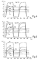
- FIGs 4-6 show graphs of voltages V P , V BOT , V B , V SB , V LC , V UP in the Figure 2 circuit for three different supply voltage V DD values.
- Each graph shows the gradual, nonimpulsive pattern of the voltages due to the delays involved; the gradual turn-on of the various components; the very small variation in bootstrap voltage V B in each case; and the manner in which V B differs in each case in relation to inverted pump voltage V P , i.e. is higher than the pump voltage when the supply voltage is low (3 V), is only slightly lower than the pump voltage when the supply voltage is medium (5 V), and differs considerably from the pump voltage when the supply voltage is high (7 V).
- the generator-booster described provides for supplying a bootstrap voltage that varies very little, even in the presence of widely differing supply voltages. Secondly, it provides for considerably reducing consumption, in that the only part supplied with current is pulse amplitude preset stage 10 via resistive transistor 20, which draws different current levels depending on the supply voltage. The other stages in fact consume and are supplied with no current, except for small capacitive peaks when switching from one step to the other. Thirdly, it is extremely straightforward in design, reliable, and easy to integrate. And fourthly, the bootstrap, turn-on and clipping voltage values may be set as required by simply sizing the transistors accordingly, or using different types of transistors (e.g. other than native).
Landscapes
- Engineering & Computer Science (AREA)
- Physics & Mathematics (AREA)
- Microelectronics & Electronic Packaging (AREA)
- General Physics & Mathematics (AREA)
- Nonlinear Science (AREA)
- Electromagnetism (AREA)
- Power Engineering (AREA)
- Radar, Positioning & Navigation (AREA)
- Automation & Control Theory (AREA)
- Dc-Dc Converters (AREA)
- Static Random-Access Memory (AREA)
- Manipulation Of Pulses (AREA)
- Logic Circuits (AREA)
Claims (12)
- Höherspannungsgenerator (1) zum Liefern eines angenähert konstanten Spannungspegels, umfassend: einen Hebekondensator (2) mit einem ersten Anschlußpunkt (3), der mit einer ersten Referenzpotentialleitung (14) verbunden ist, und einem zweiten Anschlußpunkt (4), der mit einem Anhebe-Knotenpunkt (4) verbunden ist; und eine Spannungshebe-Steuerstufe (7), die mit dem Anhebe-Knotenpunkt (4) verbunden ist und einen Pumpeingang (6) aufweist, der mit einem Pumpsignal (VPN) beliefert wird, das zwischen zwei verschiedenen Zuständen schaltbar ist, die einen Voraufladeschritt und einen Anhebeschritt des Hebekondensators bestimmen; dadurch gekennzeichnet, daß ereine Vorauflade-Begrenzungseinrichtung (13) umfaßt, die mit dem ersten Anschlußpunkt (3) des Hebekondensators (2) verbunden ist und mit einem Vorauflade-Referenzsignal (VUP) beliefert wird, und die im Voraufladeschritt dafür sorgt, die Ladung des Hebekondensators (2) auf einen Grenzwert, der auf das Vorauflade-Referenzsignal bezogen ist, zu begrenzen; und eine Begrenzerstufe (8) umfaßt, die mit dem ersten Anschlußpunkt (3) des Hebekondensators (2) verbunden ist derart, daß das Potential des ersten Anschlußpunkts des Hebekondensators beim Anhebungsschritt begrenzt wird.
- Höherspannungsgenerator nach Anspruch 1, dadurch gekennzeichnet, daß die Spannungshebe-Steuerstufe (7) Entkopplungseinrichtungen (30, 32) umfaßt, die zwischen dem Pumpeingang (6) und dem Anhebe-Knotenpunkt (4) angeordnet sind und für eine Entkopplung des Pumpeingangs vom Anhebe-Knotenpunkt dann, wenn der Anhebe-Knotenpunkt einen gegebenen Spannungswert erreicht, sorgen.
- Höherspannungsgenerator nach Anspruch 1 oder 2, dadurch gekennzeichnet, daß er eine Impulsamplituden-Voreinstellstufe (10) zum Erzeugen des Vorauflade-Referenzsignals (VUP) und eines Einschalt-Referenzsignals (VLC), das an die Begrenzerstufe (8) geliefert wird, umfaßt.
- Höherspannungsgenerator nach einem der vorhergehenden Ansprüche, dadurch gekennzeichnet, daß die Vorauflade-Begrenzungseinrichtung einen Voraufladetransistor (13) umfaßt, von dem ein erster Anschlußpunkt an die erste Bezugspotentialleitung (14) angeschlossen ist, ein zweiter Anschlußpunkt an den ersten Anschlußpunkt (3) des Hebekondensators (2) angeschlossen ist und ein Steueranschluß mit dem Vorauflade-Referenzsignal (VUP) beliefert wird.
- Höherspannungsgenerator nach Anspruch 4, dadurch gekennzeichnet, daß der Voraufladetransistor (13) ein natürlicher MOS-Transistor ist.
- Höherspannungsgenerator nach einem der vorhergehenden Ansprüche von 3 bis 5, dadurch gekennzeichnet, daß die Begrenzerstufe (8) umfaßt: einen begrenzenden Zweig (25 bis 27), der zwischen den ersten Anschlußpunkt (3) des Hebekondensators (2) und eine zweite Referenzpotentialleitung (15) geschaltet ist; einen Eingangsanschluß (12), der mit dem Einschalt-Referenzsignal (VLC) beliefert wird; und ein Einschaltelement (25, 26), das entlang dem begrenzenden Zweig eingesetzt ist; wobei das Einschaltelement (25, 26) mit dem zweiten Anschlußpunkt (4) des Hebekondensators und mit dem Eingangsanschluß (12) der Begrenzerstufe verbunden ist und den begrenzenden Zweig einschaltet, wenn die Spannung am zweiten Anschlußpunkt (4) des Hebekondensators (2) einen Wert erreicht, der durch das Einschalt-Referenzsignal bestimmt wird.
- Höherspannungsgenerator nach Anspruch 6, dadurch gekennzeichnet, daß das Einschaltelement (25, 26) einen ersten Einschalttransistor (26) und einen zweiten Einschalttransistor (25) umfaßt, die entlang dem begrenzenden Zweig (25 bis 27) eingesetzt sind, wobei der erste Einschalttransistor (26) einen Steueranschluß aufweist, der mit dem zweiten Anschlußpunkt (4) des Hebekondensators (2) verbunden ist, und der zweite Einschalttransistor (25) einen Steueranschluß aufweist, der den Eingangsanschluß (12) der Begrenzerstufe (8) bildet.
- Höherspannungsgenerator nach einem der vorhergehenden Ansprüche, dadurch gekennzeichnet, daß die Spannungshebe-Steuerstufe (7) einen ersten Entkopplungstransistor (30) und einen zweiten Entkopplungstransistor (32) umfaßt, die im Gegentakt arbeiten; wobei der erste Entkopplungstransistor (30) zwischen den zweiten Anschlußpunkt (4) des Hebekondensators (2) und eine zweite Referenzpotentialleitung (15) geschaltet ist und einen Steueranschluß aufweist, der mit dem Pumpeingang (6) verbunden ist, und der zweite Entkopplungstransistor (32) zwischen den Pumpeingang (6) und den zweiten Anschlußpunkt des Hebekondensators eingeschaltet ist und einen Steueranschluß aufweist, der mit dem ersten Anschlußpunkt (3) des Hebekondensators (2) verbunden ist.
- Höherspannungsgenerator nach Anspruch 8, dadurch gekennzeichnet, daß der erste und der zweite Entkopplungstransistor (30, 32) von gleichem Typ sind; und daß zwischen den Pumpeingang (6) und den zweiten Entkopplungstransistor (32) ein invertierendes Element (31) eingesetzt ist.
- Höherspannungsgenerator nach Anspruch 9, dadurch gekennzeichnet, daß der erste und der zweite Entkopplungstransistor (30, 32) n-Kanal-MOS-Transistoren sind.
- Höherspannungsgenerator nach einem der vorhergehenden Ansprüche von 3 bis 10, dadurch gekennzeichnet, daß die Impulsamplituden-Voreinstellstufe (10) einen Spannungseinstellzweig (20 bis 22) aufweist, der zwischen die erste Referenzpotentialleitung (14) und eine zweite Referenzpotentialleitung (15) eingeschaltet ist; und daß der Spannungseinstellzweig eine Anzahl von Konstant-Spannungsabfall-Elementen (21, 22), die in Reihe geschaltet sind, und Widerstandseinrichtungen (20), die zwischen die Konstant-Spannungsabfall-Elemente und die erste Referenzpotentialleitung (14) geschaltet sind, umfaßt.
- Höherspannungsgenerator nach Anspruch 11, dadurch gekennzeichnet, daß die Konstant-Spannungsabfall-Elemente (21, 22) diodengeschaltete Transistoren umfassen und die Widerstandseinrichtungen (20) einen MOS-Transistor umfassen.
Priority Applications (4)
| Application Number | Priority Date | Filing Date | Title |
|---|---|---|---|
| DE69518826T DE69518826T2 (de) | 1995-04-14 | 1995-04-14 | Spannungserhöhungsschaltung zur Erzeugung eines annähernd konstanten Spannungspegels |
| EP95830153A EP0737643B1 (de) | 1995-04-14 | 1995-04-14 | Spannungserhöhungsschaltung zur Erzeugung eines annähernd konstanten Spannungspegels |
| JP8091312A JP2963047B2 (ja) | 1995-04-14 | 1996-04-12 | ほぼ一定の電圧レベルを有するパルス電圧を供給する電圧発生器 |
| US08/631,574 US5914867A (en) | 1995-04-14 | 1996-04-12 | Voltage generator-booster for supplying a pulsating voltage having approximately constant voltage levels |
Applications Claiming Priority (1)
| Application Number | Priority Date | Filing Date | Title |
|---|---|---|---|
| EP95830153A EP0737643B1 (de) | 1995-04-14 | 1995-04-14 | Spannungserhöhungsschaltung zur Erzeugung eines annähernd konstanten Spannungspegels |
Publications (2)
| Publication Number | Publication Date |
|---|---|
| EP0737643A1 EP0737643A1 (de) | 1996-10-16 |
| EP0737643B1 true EP0737643B1 (de) | 2000-09-13 |
Family
ID=8221902
Family Applications (1)
| Application Number | Title | Priority Date | Filing Date |
|---|---|---|---|
| EP95830153A Expired - Lifetime EP0737643B1 (de) | 1995-04-14 | 1995-04-14 | Spannungserhöhungsschaltung zur Erzeugung eines annähernd konstanten Spannungspegels |
Country Status (4)
| Country | Link |
|---|---|
| US (1) | US5914867A (de) |
| EP (1) | EP0737643B1 (de) |
| JP (1) | JP2963047B2 (de) |
| DE (1) | DE69518826T2 (de) |
Families Citing this family (8)
| Publication number | Priority date | Publication date | Assignee | Title |
|---|---|---|---|---|
| JP4119773B2 (ja) * | 2003-03-06 | 2008-07-16 | 松下電器産業株式会社 | 半導体記憶装置および半導体装置 |
| US7365928B2 (en) * | 2004-04-14 | 2008-04-29 | Stmicroelectronics, Inc. | Write driver with improved boosting circuit and interconnect impedance matching |
| US7375909B2 (en) * | 2004-04-14 | 2008-05-20 | Stmicroelectronics, Inc. | Write driver with power optimization and interconnect impedance matching |
| US7035028B2 (en) * | 2004-05-12 | 2006-04-25 | Stmicroelectronics, Inc. | Disk drive write driver with boosting circuit to improve output voltage swing |
| TWI340981B (en) * | 2008-11-12 | 2011-04-21 | Ind Tech Res Inst | Memory with improved write current |
| JP2012075049A (ja) * | 2010-09-29 | 2012-04-12 | Dainippon Printing Co Ltd | 論理否定型電子回路 |
| US10784764B2 (en) | 2019-02-01 | 2020-09-22 | Texas Instruments Incorporated | Switched-mode DC/DC converter having a bootstrapped high-side driver |
| US11777398B2 (en) * | 2021-01-08 | 2023-10-03 | Apple Inc. | Pre-charging bootstrapped FET gate |
Family Cites Families (23)
| Publication number | Priority date | Publication date | Assignee | Title |
|---|---|---|---|---|
| GB2193392A (en) * | 1986-08-02 | 1988-02-03 | Plessey Co Plc | Efficiency enhanced voltage multiplier |
| US5051882A (en) * | 1989-01-27 | 1991-09-24 | Teledyne Industries | Three reservoir capacitor charge pump circuit |
| JPH02215154A (ja) * | 1989-02-16 | 1990-08-28 | Toshiba Corp | 電圧制御回路 |
| US5132895A (en) * | 1990-12-11 | 1992-07-21 | Motorola, Inc. | Variable charge pumping DC-to-DC converter |
| US5392205A (en) * | 1991-11-07 | 1995-02-21 | Motorola, Inc. | Regulated charge pump and method therefor |
| JPH05244766A (ja) * | 1992-02-27 | 1993-09-21 | Texas Instr Japan Ltd | チャージポンプ回路 |
| NL9201053A (nl) * | 1992-06-15 | 1994-01-03 | Koninkl Philips Electronics Nv | Switched capacitor ladingspomp, alsmede zaagtandoscillator voorzien van een dergelijke switched capacitor ladingspomp. |
| JP2806717B2 (ja) * | 1992-10-28 | 1998-09-30 | 日本電気アイシーマイコンシステム株式会社 | チャージポンプ回路 |
| US5410465A (en) * | 1993-06-11 | 1995-04-25 | Tan; Charles M. C. | Integrated circuit charge pump voltage level converter |
| DE4324855C1 (de) * | 1993-07-23 | 1994-09-22 | Siemens Ag | Ladungspumpe |
| US5386151A (en) * | 1993-08-11 | 1995-01-31 | Advanced Micro Devices, Inc. | Low voltage charge pumps using p-well driven MOS capacitors |
| US5442586A (en) * | 1993-09-10 | 1995-08-15 | Intel Corporation | Method and apparatus for controlling the output current provided by a charge pump circuit |
| EP0661795B1 (de) * | 1993-12-28 | 1997-07-16 | STMicroelectronics S.r.l. | Spannungsbooster, insbesondere für nichtflüchtige Speicher |
| JP2848235B2 (ja) * | 1994-02-28 | 1999-01-20 | 日本電気株式会社 | 半導体記憶装置用電源回路 |
| JP3148070B2 (ja) * | 1994-03-29 | 2001-03-19 | 株式会社東芝 | 電圧変換回路 |
| JP2679617B2 (ja) * | 1994-04-18 | 1997-11-19 | 日本電気株式会社 | チャージポンプ回路 |
| EP0685921B1 (de) * | 1994-05-31 | 1999-12-15 | STMicroelectronics S.r.l. | Kapazitive Ladungspumpe, Bicmos Schaltung für niedrige Versorgungsspannung |
| GB9423038D0 (en) * | 1994-11-15 | 1995-01-04 | Sgs Thomson Microelectronics | An integrated circuit memory device with voltage boost |
| US5694308A (en) * | 1995-07-03 | 1997-12-02 | Motorola, Inc. | Method and apparatus for regulated low voltage charge pump |
| US5708387A (en) * | 1995-11-17 | 1998-01-13 | Advanced Micro Devices, Inc. | Fast 3-state booster-circuit |
| US5680300A (en) * | 1995-12-22 | 1997-10-21 | Analog Devices, Inc. | Regulated charge pump DC/DC converter |
| US5808883A (en) * | 1996-02-15 | 1998-09-15 | Harris Corporation | DC-to-DC converter having charge pump and associated methods |
| US5831845A (en) * | 1998-03-31 | 1998-11-03 | Xilinx, Inc. | Voltage regulator with charge pump and parallel reference nodes |
-
1995
- 1995-04-14 EP EP95830153A patent/EP0737643B1/de not_active Expired - Lifetime
- 1995-04-14 DE DE69518826T patent/DE69518826T2/de not_active Expired - Lifetime
-
1996
- 1996-04-12 US US08/631,574 patent/US5914867A/en not_active Expired - Lifetime
- 1996-04-12 JP JP8091312A patent/JP2963047B2/ja not_active Expired - Fee Related
Also Published As
| Publication number | Publication date |
|---|---|
| EP0737643A1 (de) | 1996-10-16 |
| US5914867A (en) | 1999-06-22 |
| JP2963047B2 (ja) | 1999-10-12 |
| DE69518826T2 (de) | 2001-02-22 |
| JPH0923141A (ja) | 1997-01-21 |
| DE69518826D1 (de) | 2000-10-19 |
Similar Documents
| Publication | Publication Date | Title |
|---|---|---|
| JP3256732B2 (ja) | プログラム可能なメモリのためのプログラミング電圧調整回路 | |
| US5039877A (en) | Low current substrate bias generator | |
| US5892390A (en) | Internal power supply circuit with low power consumption | |
| JP2638533B2 (ja) | 不揮発性メモリ用電圧ブースタ | |
| US6137335A (en) | Oscillator receiving variable supply voltage depending on substrate voltage detection | |
| US4717840A (en) | Voltage level sensing power-up reset circuit | |
| KR100948902B1 (ko) | 비휘발성 메모리용 전압부스터 | |
| KR960003529B1 (ko) | 반도체 메모리 장치의 칩 초기화 신호 발생회로 | |
| US5796285A (en) | Voltage-limiting circuit with hysteresis comparator | |
| US6005434A (en) | Substrate potential generation circuit that can suppress variation of output voltage with respect to change in external power supply voltage and environment temperature | |
| KR19980071694A (ko) | 승압 회로 및 반도체 기억 장치 | |
| EP0737643B1 (de) | Spannungserhöhungsschaltung zur Erzeugung eines annähernd konstanten Spannungspegels | |
| US4385245A (en) | MOS Power-on reset circuit | |
| US4384216A (en) | Controlled power performance driver circuit | |
| EP0433724B1 (de) | Spannungsregler mit Leistungszusatzsystem | |
| US6559710B2 (en) | Raised voltage generation circuit | |
| KR100401392B1 (ko) | 전압조절회로및그방법,조절된전압조절회로및메모리회로 | |
| US6989704B2 (en) | Delay circuit having function of filter circuit | |
| US5523710A (en) | Initial value setting circuit | |
| US6163468A (en) | Start up circuits and bias generators | |
| US6346835B1 (en) | Power-on reset signal preparing circuit | |
| US6380800B1 (en) | Pump area reduction through the use of passive RC-filters or active filters | |
| US5739719A (en) | Bias circuit with low sensitivity to threshold variations | |
| EP0507502A2 (de) | Hochspannungsladungspumpen | |
| US4611134A (en) | Bootstrap driving circuit |
Legal Events
| Date | Code | Title | Description |
|---|---|---|---|
| PUAI | Public reference made under article 153(3) epc to a published international application that has entered the european phase |
Free format text: ORIGINAL CODE: 0009012 |
|
| AK | Designated contracting states |
Kind code of ref document: A1 Designated state(s): DE FR GB IT |
|
| 17P | Request for examination filed |
Effective date: 19970409 |
|
| RAP3 | Party data changed (applicant data changed or rights of an application transferred) |
Owner name: STMICROELECTRONICS S.R.L. |
|
| GRAG | Despatch of communication of intention to grant |
Free format text: ORIGINAL CODE: EPIDOS AGRA |
|
| 17Q | First examination report despatched |
Effective date: 19990816 |
|
| GRAG | Despatch of communication of intention to grant |
Free format text: ORIGINAL CODE: EPIDOS AGRA |
|
| GRAH | Despatch of communication of intention to grant a patent |
Free format text: ORIGINAL CODE: EPIDOS IGRA |
|
| GRAH | Despatch of communication of intention to grant a patent |
Free format text: ORIGINAL CODE: EPIDOS IGRA |
|
| GRAA | (expected) grant |
Free format text: ORIGINAL CODE: 0009210 |
|
| AK | Designated contracting states |
Kind code of ref document: B1 Designated state(s): DE FR GB IT |
|
| REF | Corresponds to: |
Ref document number: 69518826 Country of ref document: DE Date of ref document: 20001019 |
|
| ET | Fr: translation filed | ||
| ITF | It: translation for a ep patent filed | ||
| PLBE | No opposition filed within time limit |
Free format text: ORIGINAL CODE: 0009261 |
|
| STAA | Information on the status of an ep patent application or granted ep patent |
Free format text: STATUS: NO OPPOSITION FILED WITHIN TIME LIMIT |
|
| 26N | No opposition filed | ||
| REG | Reference to a national code |
Ref country code: GB Ref legal event code: IF02 |
|
| PGFP | Annual fee paid to national office [announced via postgrant information from national office to epo] |
Ref country code: GB Payment date: 20080326 Year of fee payment: 14 |
|
| PGFP | Annual fee paid to national office [announced via postgrant information from national office to epo] |
Ref country code: IT Payment date: 20080409 Year of fee payment: 14 |
|
| GBPC | Gb: european patent ceased through non-payment of renewal fee |
Effective date: 20090414 |
|
| REG | Reference to a national code |
Ref country code: FR Ref legal event code: ST Effective date: 20091231 |
|
| PG25 | Lapsed in a contracting state [announced via postgrant information from national office to epo] |
Ref country code: GB Free format text: LAPSE BECAUSE OF NON-PAYMENT OF DUE FEES Effective date: 20090414 Ref country code: FR Free format text: LAPSE BECAUSE OF NON-PAYMENT OF DUE FEES Effective date: 20091222 |
|
| PGFP | Annual fee paid to national office [announced via postgrant information from national office to epo] |
Ref country code: FR Payment date: 20080429 Year of fee payment: 14 |
|
| PG25 | Lapsed in a contracting state [announced via postgrant information from national office to epo] |
Ref country code: IT Free format text: LAPSE BECAUSE OF NON-PAYMENT OF DUE FEES Effective date: 20090414 |
|
| REG | Reference to a national code |
Ref country code: DE Ref legal event code: R082 Ref document number: 69518826 Country of ref document: DE Representative=s name: BOEHMERT & BOEHMERT, DE |
|
| REG | Reference to a national code |
Ref country code: DE Ref legal event code: R082 Ref document number: 69518826 Country of ref document: DE Representative=s name: BOEHMERT & BOEHMERT ANWALTSPARTNERSCHAFT MBB -, DE Effective date: 20131209 Ref country code: DE Ref legal event code: R082 Ref document number: 69518826 Country of ref document: DE Representative=s name: BOEHMERT & BOEHMERT, DE Effective date: 20131209 Ref country code: DE Ref legal event code: R081 Ref document number: 69518826 Country of ref document: DE Owner name: MICRON TECHNOLOGY, INC., BOISE, US Free format text: FORMER OWNER: STMICROELECTRONICS S.R.L., AGRATE BRIANZA, MAILAND/MILANO, IT Effective date: 20131209 Ref country code: DE Ref legal event code: R081 Ref document number: 69518826 Country of ref document: DE Owner name: MICRON TECHNOLOGY, INC., US Free format text: FORMER OWNER: STMICROELECTRONICS S.R.L., AGRATE BRIANZA, IT Effective date: 20131209 |
|
| PGFP | Annual fee paid to national office [announced via postgrant information from national office to epo] |
Ref country code: DE Payment date: 20140430 Year of fee payment: 20 |
|
| REG | Reference to a national code |
Ref country code: DE Ref legal event code: R071 Ref document number: 69518826 Country of ref document: DE |