EP0735520B1 - Helligkeitsregelung in einer Flüssigkristallanzeigeeinrichtung mit Kompensation der Nichtlinearität - Google Patents
Helligkeitsregelung in einer Flüssigkristallanzeigeeinrichtung mit Kompensation der Nichtlinearität Download PDFInfo
- Publication number
- EP0735520B1 EP0735520B1 EP96103005A EP96103005A EP0735520B1 EP 0735520 B1 EP0735520 B1 EP 0735520B1 EP 96103005 A EP96103005 A EP 96103005A EP 96103005 A EP96103005 A EP 96103005A EP 0735520 B1 EP0735520 B1 EP 0735520B1
- Authority
- EP
- European Patent Office
- Prior art keywords
- signal
- liquid crystal
- counter electrode
- image signal
- voltage
- Prior art date
- Legal status (The legal status is an assumption and is not a legal conclusion. Google has not performed a legal analysis and makes no representation as to the accuracy of the status listed.)
- Expired - Lifetime
Links
Images


Classifications
-
- G—PHYSICS
- G09—EDUCATION; CRYPTOGRAPHY; DISPLAY; ADVERTISING; SEALS
- G09G—ARRANGEMENTS OR CIRCUITS FOR CONTROL OF INDICATING DEVICES USING STATIC MEANS TO PRESENT VARIABLE INFORMATION
- G09G3/00—Control arrangements or circuits, of interest only in connection with visual indicators other than cathode-ray tubes
- G09G3/20—Control arrangements or circuits, of interest only in connection with visual indicators other than cathode-ray tubes for presentation of an assembly of a number of characters, e.g. a page, by composing the assembly by combination of individual elements arranged in a matrix no fixed position being assigned to or needed to be assigned to the individual characters or partial characters
- G09G3/22—Control arrangements or circuits, of interest only in connection with visual indicators other than cathode-ray tubes for presentation of an assembly of a number of characters, e.g. a page, by composing the assembly by combination of individual elements arranged in a matrix no fixed position being assigned to or needed to be assigned to the individual characters or partial characters using controlled light sources
- G09G3/30—Control arrangements or circuits, of interest only in connection with visual indicators other than cathode-ray tubes for presentation of an assembly of a number of characters, e.g. a page, by composing the assembly by combination of individual elements arranged in a matrix no fixed position being assigned to or needed to be assigned to the individual characters or partial characters using controlled light sources using electroluminescent panels
- G09G3/32—Control arrangements or circuits, of interest only in connection with visual indicators other than cathode-ray tubes for presentation of an assembly of a number of characters, e.g. a page, by composing the assembly by combination of individual elements arranged in a matrix no fixed position being assigned to or needed to be assigned to the individual characters or partial characters using controlled light sources using electroluminescent panels semiconductive, e.g. using light-emitting diodes [LED]
-
- G—PHYSICS
- G09—EDUCATION; CRYPTOGRAPHY; DISPLAY; ADVERTISING; SEALS
- G09G—ARRANGEMENTS OR CIRCUITS FOR CONTROL OF INDICATING DEVICES USING STATIC MEANS TO PRESENT VARIABLE INFORMATION
- G09G3/00—Control arrangements or circuits, of interest only in connection with visual indicators other than cathode-ray tubes
- G09G3/20—Control arrangements or circuits, of interest only in connection with visual indicators other than cathode-ray tubes for presentation of an assembly of a number of characters, e.g. a page, by composing the assembly by combination of individual elements arranged in a matrix no fixed position being assigned to or needed to be assigned to the individual characters or partial characters
- G09G3/34—Control arrangements or circuits, of interest only in connection with visual indicators other than cathode-ray tubes for presentation of an assembly of a number of characters, e.g. a page, by composing the assembly by combination of individual elements arranged in a matrix no fixed position being assigned to or needed to be assigned to the individual characters or partial characters by control of light from an independent source
- G09G3/36—Control arrangements or circuits, of interest only in connection with visual indicators other than cathode-ray tubes for presentation of an assembly of a number of characters, e.g. a page, by composing the assembly by combination of individual elements arranged in a matrix no fixed position being assigned to or needed to be assigned to the individual characters or partial characters by control of light from an independent source using liquid crystals
- G09G3/3611—Control of matrices with row and column drivers
- G09G3/3648—Control of matrices with row and column drivers using an active matrix
- G09G3/3655—Details of drivers for counter electrodes, e.g. common electrodes for pixel capacitors or supplementary storage capacitors
-
- G—PHYSICS
- G09—EDUCATION; CRYPTOGRAPHY; DISPLAY; ADVERTISING; SEALS
- G09G—ARRANGEMENTS OR CIRCUITS FOR CONTROL OF INDICATING DEVICES USING STATIC MEANS TO PRESENT VARIABLE INFORMATION
- G09G3/00—Control arrangements or circuits, of interest only in connection with visual indicators other than cathode-ray tubes
- G09G3/20—Control arrangements or circuits, of interest only in connection with visual indicators other than cathode-ray tubes for presentation of an assembly of a number of characters, e.g. a page, by composing the assembly by combination of individual elements arranged in a matrix no fixed position being assigned to or needed to be assigned to the individual characters or partial characters
- G09G3/34—Control arrangements or circuits, of interest only in connection with visual indicators other than cathode-ray tubes for presentation of an assembly of a number of characters, e.g. a page, by composing the assembly by combination of individual elements arranged in a matrix no fixed position being assigned to or needed to be assigned to the individual characters or partial characters by control of light from an independent source
- G09G3/36—Control arrangements or circuits, of interest only in connection with visual indicators other than cathode-ray tubes for presentation of an assembly of a number of characters, e.g. a page, by composing the assembly by combination of individual elements arranged in a matrix no fixed position being assigned to or needed to be assigned to the individual characters or partial characters by control of light from an independent source using liquid crystals
- G09G3/3611—Control of matrices with row and column drivers
- G09G3/3648—Control of matrices with row and column drivers using an active matrix
-
- G—PHYSICS
- G09—EDUCATION; CRYPTOGRAPHY; DISPLAY; ADVERTISING; SEALS
- G09G—ARRANGEMENTS OR CIRCUITS FOR CONTROL OF INDICATING DEVICES USING STATIC MEANS TO PRESENT VARIABLE INFORMATION
- G09G2320/00—Control of display operating conditions
- G09G2320/02—Improving the quality of display appearance
- G09G2320/0271—Adjustment of the gradation levels within the range of the gradation scale, e.g. by redistribution or clipping
- G09G2320/0276—Adjustment of the gradation levels within the range of the gradation scale, e.g. by redistribution or clipping for the purpose of adaptation to the characteristics of a display device, i.e. gamma correction
-
- G—PHYSICS
- G09—EDUCATION; CRYPTOGRAPHY; DISPLAY; ADVERTISING; SEALS
- G09G—ARRANGEMENTS OR CIRCUITS FOR CONTROL OF INDICATING DEVICES USING STATIC MEANS TO PRESENT VARIABLE INFORMATION
- G09G3/00—Control arrangements or circuits, of interest only in connection with visual indicators other than cathode-ray tubes
- G09G3/20—Control arrangements or circuits, of interest only in connection with visual indicators other than cathode-ray tubes for presentation of an assembly of a number of characters, e.g. a page, by composing the assembly by combination of individual elements arranged in a matrix no fixed position being assigned to or needed to be assigned to the individual characters or partial characters
- G09G3/2007—Display of intermediate tones
- G09G3/2011—Display of intermediate tones by amplitude modulation
Definitions
- the present invention relates to a liquid crystal display device, such as a liquid crystal television set and a liquid crystal display, having a brightness adjusting function and being provided with pixels at crossing points of row electrodes and column electrodes in a matrix form.
- TFT-LCD Thin Film Transistors
- the TFT-LCD as shown in Fig. 12, has a liquid crystal panel 51 having:
- the source drive circuit 57 receives a control signal from a drive control circuit (not shown) as well as an image signal (described later). Based on a sampling pulse of the control signal synchronizing with a horizontally synchronizing signal, the image signal which corresponds to one horizontal scanning period is transmitted to a sample & hold circuit 60 through a shift resistor 59, and then outputted to each of the signal electrodes 52 through an output buffer 61.
- the gate drive circuit 58 receives a control signal from the drive control circuit. Based on the control signal synchronizing with a horizontally synchronizing signal, a gate-on signal is transmitted to a level shifter 53 as the gate-on signal is sequentially shifted by a shift resistor 62. The gate-on signal is then converted by the level shifter 63 to reach a level which can turn on the TFTs 55, and outputted to each of the gate electrodes 53 through an output buffer 64.
- the TFTs 55 on the gate electrodes 53 are turned on sequentially, and a signal voltage Vs of the image signal is applied to the pixel electrodes 54.
- a counter voltage Vcom as a counter electrode signal generated in a counter electrode signal generating circuit 71 is applied to the counter electrode 56 which is provided opposite to the pixel electrodes 54 with respect to the liquid crystal layer (See Fig. 15).
- the AC-Drive method employs a counter electrode signal of alternating current which can reduce the peak-to-peak amplitude of the whole image signal, while maintaining the difference between the counter voltage Vcom and the signal voltage Vs, i.e., the drive voltage V for the liquid crystal.
- the liquid crystal display device such as a liquid crystal television set and a liquid crystal display, is normally provided with a brightness adjusting function to compensate the viewing angle characteristics.
- the liquid crystal display device can adjust the brightness so as to suit an environment in which the liquid crystal display device is used.
- Such brightness adjustment is conventionally, as shown in Fig. 13, carried out by changing a voltage level of the image signal which corresponds to one horizontal scanning period.
- the change in the voltage level of the image signal causes a change in the whole voltage difference between the image signal and the counter electrode signal, i.e., the drive voltage V applied to the liquid crystal.
- the brightness of the display can be changed.
- the change in the voltage level of the image signal invariably causes a change in the peak-to-peak amplitude of the whole image signal. Therefore, a driver IC with high withstand voltage, or a so-called medium withstand-voltage driver IC, should be used as a driver IC of the source drive circuit 57.
- the medium withstand-voltage driver IC has deficiencies compared with an ordinary low withstand-voltage driver IC in terms of chip size and cost. As a result, the medium withstand-voltage driver IC may be an obstacle in making a smaller and thinner TFT-LCD module and may further cause a cost increase of the TFT-LCD.
- the present inventors in order to solve the problems and make it possible to use the low withstand-voltage driver IC as the driver IC of the source drive circuit 57, proposed a different method of adjusting the brightness of the display as disclosed in Japanese Laid-Open Patent Application No. 7-295164/1995 (hereafter referred to as the voltage-lowering method).
- the disclosed voltage-lowering method changes the voltage level of the counter electrode signal corresponding to one horizontal line period as shown in Fig. 14, instead of changing the voltage level of the image signal corresponding to one horizontal line period.
- the voltage-lowering method thus changes the voltage difference between the image signal and the counter electrode signal, thereby changing the brightness of the display.
- a user sets a target brightness through a brightness adjusting section 72 for setting the brightness of the display.
- a brightness control signal in accordance with the target brightness is sent from the brightness adjusting section 72 to the counter electrode signal generating circuit 71.
- the counter electrode signal generating circuit 71 generates the counter electrode signal by amplifying a polarity inverting signal in accordance with the brightness control signal through a feedback amplifying circuit (not shown) which is part of an amplitude adjusting section.
- a feedback amplifying circuit not shown
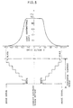
- the light transmittance index has unique characteristics as shown in Fig. 7. Therefore, it is necessary to carry out a compensation with respect to the image signal in accordance with the characteristics in order to achieve good gradation.
- this type of compensation is called a gamma control.
- the image signal is adjusted in terms of brightness in order to be inputted into a liquid crystal module like the one above.
- the gamma control compensates the voltage applied to the liquid crystal in accordance with the level of the adjusted image signal.
- Fig. 8 shows characteristics of the transmittance index after the voltage applied to the liquid crystal, i.e., the drive voltage, is compensated to be proportional to the transmittance index.
- the characteristics shown in Figs. 7 and 8 are represented as A and B respectively, B is obtainable by compensating A, in other words, by multiplying A by a compensation factor 'B ⁇ A'.
- Fig. 9 shows transmittance-drive voltage characteristics of the compensation factor in accordance with this idea (hereafter referred to as compensation characteristics).
- the drive voltage becomes proportional to the transmittance index as shown in Fig. 8 by converting the level of the image signal in accordance with the compensation characteristics.
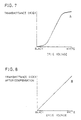
- the ideal compensation characteristics can be substituted for by polygonal-line approximation characteristics having two inflection points ⁇ 1 and ⁇ 2 as shown in Fig. 10. Therefore, the level of the image signal is, in practice, converted in accordance with the polygonal-line approximation characteristics.
- the inflection point voltages ⁇ 1 and ⁇ 2 of this type of polygonal-line approximation characteristics are determined on the basis of a certain reference value of the image signal.
- the good gradation can be obtained with the TFT-LCD which changes the brightness by changing the voltage level of the image signal corresponding to one horizontal line period.
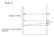
- the condition is, as shown in Fig. 16, that the inflection point voltages ⁇ 1 and ⁇ 2 of the polygonal-line approximation characteristics are determined on the basis of an off-set point L of the counter electrode signal, or in other words, on the basis of a reference point of the image signal.
- the inflection point voltages ⁇ 1 and ⁇ 2 do not change even if the voltage level of the image signal changes and causes a voltage change as much as variation ⁇ .
- the good gradation can be maintained.
- the above TFT-LCD employing the voltage-lowering method changes the amplitude of the counter electrode signal, instead of changing the voltage level of the image signal corresponding to one horizontal line period. Such a change in the amplitude then changes the drive voltage applied to the liquid crystal, thereby changing the brightness of the display. Therefore, as shown in Fig. 17, the voltage-lowering method has a problem if the inflection point voltages ⁇ 1 and ⁇ 2 of the polygonal-line approximation characteristics are determined on the basis of the off-set point L of the counter electrode signal, or in other words, on-the basis of the reference point of the image signal.
- prior art document US-A-5,298,892 describes a display panel system comprising a stacked display panel and drive units therefor.
- the drive units include a computer for adjusting for the individual gamma characteristics of each one of the display panels for color balancing purposes and for causing the luminance of each panel to be maximized, or at least greatly increased for each intensity level or shading of each color.
- Prior art document JP-A-4320296 describes a liquid crystal display device, wherein analog signals corresponding to respective colors of column electrodes are inputted to picture elements of a liquid crystal panel corresponding to respective colors, and a voltage is applied between the electrodes and a counter electrode to apply a voltage to a liquid crystal display element finally.
- a LC brightness correcting circuit which converts an input signal in consideration of the nonlinearity of the liquid crystal so that the brightness characteristic varies linearly sets an input-output characteristic which is right opposite from the transmissivity-voltage characteristic of the liquid crystal to set the transmissivity of the liquid crystal so that the transmissivity varies linearly with the respective color signal inputs of red, blue, and green.
- the LC brightness correcting circuit is provided for each of the respective color signals, and converting circuits and inverting circuits for adjusting the levels and amplitudes of the analog signals for the respective colors suitably for driving the liquid crystal are constituted individually as well.
- prior art document JP-A-6027901 discloses a liquid crystal display device, wherein a common voltage inverted in polarity alternately in synchronism with an inversion control signal is applied to a common electrode of a liquid crystal. Further, potential differences between eight kinds of specific gradation voltages selected corresponding to display data are more expanded than other potential differences so that the quantity of variation in transmissivity in the vicinity of a black level having a problem in linearity can be made large corresponding to the potential differences, and the variation in gradation almost at the black level can be made distinctive.
- the present invention provides a liquid crystal display device as specified in claim 1.
- the reference value shifting section provided in the image signal generating means shifts the reference value of the compensation characteristics as much as the variation of the counter electrode signal amplitude which is adjusted on the basis of the setting through the brightness setting section.
- the level conversion section of an image signal compensation section converts the level of the image signal in accordance with the compensation characteristics for compensating the non-linearity of the transmittance index of the liquid crystal to the applied voltage.
- the counter electrode signal generating means provided with the amplitude adjusting section, can adjust the amplitude of the counter electrode signal on the basis of the setting through the brightness setting section. The arrangement thus changes the voltage applied to the liquid crystal (the drive voltage) and changes the display brightness.
- the liquid crystal display device in accordance with the present invention is small, thin and cheap, and can produce the correct gradation despite having the display brightness adjusting function.
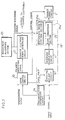
- a liquid crystal display device of the present embodiment is of an active matrix drive system type which uses TFTs 5 as switching elements (hereafter, simply referred to as a TFT-LCD).
- TFT-LCD active matrix drive system type which uses TFTs 5 as switching elements
- a Normally-White TFT-LCD will be explained.
- the Normally-White TFT-LCD normally lets light pass therethrough, but blockades light when a voltage is applied thereto.
- the TFT-LCD has a TFT substrate provided with TFTs 5 in a matrix form, a counter substrate provided opposite to the TFT substrate, and a liquid crystal panel 1 having liquid crystal layer provided between the TFT and counter substrates and two polarizing plates.
- signal electrodes 2 and gate electrodes 3 are provided to cross with each other at right angles.
- the signal electrodes 2 and the gate electrodes 3 are made of transparent conductive films and of a stripe-like shape. Near crossing points of the signal electrodes 2 and the gate electrodes 3 on the TFT substrate, the TFTs 5 and pixel electrodes (display electrodes) 4 are provided.
- the pixel electrodes 4 are made of transparent conductive films.
- Each source of the TFTs 5 is connected to each of the signal electrodes 2.
- Each drain of the TFTs 5 is connected to each of the pixel electrodes 4.
- Each gate of the TFTs 5 is connected to each of the gate electrodes 3.
- On the counter substrate a counter electrode 6 is provided.
- the counter electrode 6 is made of a transparent conductive film.
- the liquid crystal panel 1 is driven by a source drive circuit (signal voltage applying means) 7 which is connected to the signal electrodes 2 and a gate drive circuit 8 which is connected to the gate electrodes 3.
- a source drive circuit (signal voltage applying means) 7 which is connected to the signal electrodes 2
- a gate drive circuit 8 which is connected to the gate electrodes 3.
- the source drive circuit 7 is a low withstand-voltage driver IC which is mainly composed of a shift resistor 9, a sample & hold circuit 10 and an output buffer 11.
- a power source device (not shown) provides power supply to the source drive circuit 7.
- the source drive circuit 7 receives an image signal from a video interface 19 and receives a control signal from a drive control circuit 20.
- the video interface 19 will be, hereafter, referred to as simply the video I/F 19 and explained later in detail.
- the gate drive circuit 8 is basically composed of a shift resistor 12, a level shifter 13 and an output buffer 14.
- the power source device provides power supply to the gate drive circuit 8.
- the gate drive circuit 8 receives a control signal from the drive control circuit 20.
- a counter voltage Vcom (a counter electrode signal generated by a counter electrode signal generating circuit 21 shown in Fig. 1) is applied to the counter electrode 6 which is provided opposite to the pixel electrodes 4 with respect to the liquid crystal layer.
- the counter electrode signal generating circuit 21 generates a counter electrode signal by amplifying a polarity inverting signal (see Fig. 4(b)) through a feedback amplifying circuit (amplitude adjustment section) 21a (see Fig. 3).
- An example of the counter electrode signal thus generated by the counter electrode signal generating circuit 21 is shown in Fig. 4(c).
- the polarity inverting signal here is generated by the drive control circuit 20 and has a pulse width corresponding to one horizontal scanning period.
- the feedback amplifying circuit 21a is composed of resistors R1 and R2, variable resistor VR and an amplifier 22.
- the amplifier 22 receives a DC voltage at a positive input terminal thereof and receives the polarity inverting signal through the resistor R1 at a negative input terminal thereof.
- An output of the amplifier 22 is fed back into the negative input terminal of the amplifier 22 through the resistor R2 and the variable resistor VR.
- the resistor R2 and the variable resistor VR are connected in series with each other. Consequently, it is possible to change the output of the amplifier 22, i.e., a peak-to-peak amplitude of the counter electrode signal, by changing a resistance value of the variable resistor VR. Examples of the counter electrode signal output from the amplifier 22 are shown in Figs. 4(c) through 4(e).
- the resistance value of the variable resistor VR is determined by a brightness control signal in accordance with brightness set through a brightness adjusting section (brightness setting section) 23 (see Fig. 1).
- the brightness adjusting section 23 is provided on an outer surface of a device.
- the TFT-LCD is provided with the video I/F (image signal generating means) 19.
- the video I/F 19 generates the image signal of a waveform suitable for driving the liquid crystal by processing the inputted image signal separated from, for example, a television signal.
- the video I/F 19, as shown in Fig. 1, has a pedestal clamp circuit 16, an inversion amplifying circuit 17 and a gamma control section (image signal compensation section) 25.
- the pedestal clamp circuit 16 makes pedestal level of the image signal constant.
- the inversion amplifying circuit 17 inverts polarity of the image signal at a predetermined frequency (one frequency equals to one reciprocal of the horizontal scanning period).
- the gamma control section 25 carries out a gamma control with respect to the image signal.
- the image signal is outputted to the source drive circuit 7 through the video I/F 19.
- the gamma compensation section 25, which carries out the so-called gamma control, is made up of a level conversion section 25a and a reference value shifting section 25b.
- the level conversion section 25a converts the level of the image signal from the inversion amplifying circuit 17.
- the level conversion is carried out in accordance with a polygonal-line approximation characteristics having inflection points ⁇ 1 and ⁇ 2 as shown in Fig. 10.
- the voltage levels of the inflection points ⁇ 1 and ⁇ 2 are determined on the basis of a variable reference value which changes in accordance with a variation of the counter electrode signal amplitude.
- Fig. 8 shows characteristics of the transmittance index after the compensation is carried out so that the drive voltage applied to the liquid crystal becomes proportional to the transmittance index.
- the characteristics shown in Figs. 7 and 8 are represented as A and B respectively, B is obtainable by compensating A, in other words, by multiplying A by a compensation factor 'B ⁇ A'.
- Fig. 9 shows transmittance-drive voltage characteristics of the compensation factor in accordance with this idea.
- the drive voltage becomes proportional to the transmittance index as shown in Fig. 8 by converting the level of the image signal in accordance with the compensation characteristics.
- a very complex circuit is needed in order to carry out the compensation which exactly incorporates these compensation characteristics as shown in Fig. 9. Therefore, the compensation is carried out approximately with respect to the light transmittance index characteristics of the liquid crystal.
- the level of the image signal is converted in accordance with the polygonal-line approximation characteristics having the inflection points ⁇ 1 and ⁇ 2 as shown in Fig. 10.
- the number of inflection points may be more than two. The more inflection points are employed, the closer the actual compensation is to the ideal compensation as shown in Fig. 9.
- the reference value shifting section 25b changes the reference value of the polygonal-line approximation characteristics employed by the level conversion section 25a.
- the reference value shifting section 25b carries out this change on the basis of the brightness control signal in accordance with the brightness set through the brightness setting section 23.
- the reference value shifts together with a variation of the counter electrode signal amplitude.
- the reference value shifting section 25b shifts the reference value in a direction opposite to the above shift direction, thus causing the reference value to be maintained at a constant value.
- the reference value of the polygonal-line approximation characteristics is shifted as much as variation ⁇ of the counter electrode signal.
- the variation ⁇ is in accordance with the brightness control signal sent from the brightness setting section 23.
- the inflection points ⁇ 1 and ⁇ 2 of the polygonal-line approximation characteristics are fixed at a predetermined voltage level as shown in Fig. 11.
- the shift of the reference value is necessary for the following reasons.
- the peak-to-peak amplitude of the counter electrode signal varies, for example as in Figs. 4(c) to 4(e), as the setting of the variable resistor VR of the counter electrode signal generating circuit 21 changes in accordance with the brightness control signal sent from the brightness setting section 23.
- the varying amplitude results in a shift of the off-set point L of the counter electrode signal, or in other words, in a shift of the reference point of the image signal.
- the inflection points ⁇ 1 and ⁇ 2 also shift according to the shift of the off-set point L. Hence, it is impossible to carry out a correct compensation in accordance with the drive voltage.
- the TFT-LCD has a synchronization separation circuit 24 and the drive control circuit 20.
- the synchronization separation circuit 24 separates the synchronizing signal from the inputted image signal.
- the drive control circuit 20, on the basis of the synchronizing signal sent from the synchronization separation circuit 24, generates various signals: for example, the control signal for controlling operations of the source drive circuit 7 and the gate drive circuit 8, the polarity inverting signal supplied to the counter electrode signal generating circuit 21, and a gate pulse for clamping a pedestal level portion of the image signal.
- the original image signal separated from, for example, a television signal is inputted to the video I/F 19 and the synchronization separation circuit 24.
- the synchronization separation circuit 24 separates horizontally and vertically synchronizing signals from the original image signal and outputs the horizontally and vertically synchronizing signals to the drive control circuit 20.
- the drive control circuit 20 forms the gate pulse for clamping the pedestal level portion of the image signal and outputs the gate pulse to the pedestal clamp circuit 16 of the video I/F 19.
- the drive control circuit 20 utilizes a delay circuit (not shown) and delays for a predetermined time the horizontally synchronizing signal sent from the synchronization separation circuit 24.
- the pedestal level portion of the image signal is maintained at a constant value by the pedestal clamp circuit 16. Then, the polarity of the image signal is inverted at a predetermined frequency by the inversion amplifying circuit 17.
- the image signal input has a waveform, for example, as in Fig. 4(a).
- level difference between the black level and the white level of the image signal outputted from the inversion amplifying circuit 17 i.e., the peak-to-peak amplitude of the whole image signal
- the light transmittance index in accordance with the light transmittance index characteristics of the liquid crystal shown in Fig. 5 can vary between maximum and minimum values.
- the image signal outputted from the inversion amplifying circuit 17 is supplied to the gamma compensation section 25.
- the level of the image signal is converted by the level conversion section 25a in accordance with the polygonal-line approximation characteristics having the inflection points ⁇ 1 and ⁇ 2 as shown in Fig. 10.
- the inflection points ⁇ 1 and ⁇ 2 are fixed at constant voltage levels respectively, even if the amplitude of the counter electrode signal varies. This is because the reference value of the polygonal-line approximation characteristics is shifted by the reference value shifting section 25b according to the inputted brightness control signal.
- the off-set point L of the counter electrode signal is shifted as much as the variation ⁇ in accordance with the amplitude variation of the counter electrode signal responding to the brightness control signal as shown in Fig. 11.
- the reference value shifting section 25b shifts the reference value of the polygonal-line approximation characteristics as much as the variation ⁇ to the direction opposite to the shift direction of the off-set point L.
- the inflection points ⁇ 1 and ⁇ 2 are respectively fixed at constant voltage levels regardless of the amplitude variation of the counter electrode signal as shown in Fig. 11.
- the image signal formed by the video I/F 19 is then supplied to the source drive circuit 7.
- the source drive circuit 7 receives the control signal from the drive control circuit 20 as well as the above image signal. Based on a sampling pulse of the control signal in synchronism with the horizontally synchronizing signal, the image signal corresponding to one horizontal scanning period is transmitted to the sample & hold circuit 10 through the shift resistor 9, and then outputted to each of the signal electrodes 2 through the output buffer 11 as shown in Fig. 2.
- the gate drive circuit 8 receives the control signal from the drive control circuit 20. Based on the control signal, a gate-on signal is transmitted to the level shifter 13 as the gate-on signal shifts in the shift resistor 12 sequentially. The gate-on signal is then converted in the level shifter 13 to reach a level capable of turning on the TFTs 5, and outputted to each of the gate electrodes 3 through the output buffer 14.
- the drive control circuit 20 generates the polarity inverting signal with the pulse width corresponding to one horizontal scanning period as shown in Fig. 4 (b).
- the polarity inverting signal is outputted to the counter electrode signal generating circuit 21.
- the brightness adjusting section 23 sends the brightness control signal to the counter electrode signal generating circuit 21.
- the brightness control signal changes the setting of the variable resistor VR of the counter electrode signal generating circuit 21 shown in Fig. 3.
- the change in the setting changes a gain of the feedback amplifying circuit 21a.
- the feedback amplifying circuit 21a then generates and outputs the counter electrode signal with the varying peak-to-peak amplitude. Examples of such counter electrode signals are shown in Figs. 4(c) to 4(e).
- the counter electrode signal thus generated is supplied to the counter electrode 6 provided opposite to the pixel electrodes 4 with respect to the liquid crystal layer.
- Figs. 4(a) to 4(e) show waveforms of the signals upon being supplied to the source drive circuit 7.
- a time when the image signal is supplied to the pixel electrodes 4 differs from a time when the signals are supplied to the source drive circuit 7. The time difference corresponds to one horizontal scanning period and is caused by a sampling hold operation of the source drive circuit 7.
- Figs. 6(a) to 6(c) show the image signal in Fig. 4(a) overlapping with the counter electrode signals in Figs. 4(c) to 4(e) at a time when the signal voltage Vs and the counter voltage Vcom are applied to the liquid crystal layer.
- the TFT-LCD of the embodiment employs the arrangement where the peak-to-peak amplitude of the counter electrode signal generated by the counter electrode signal generating circuit 21 changes according to the brightness control signal sent from the brightness adjusting section 23.
- the reference value shifting section 25b of the gamma control section 25 provided in the video I/F 19 shifts the reference value of the polygonal-line approximation characteristics as much as the amplitude variation ⁇ of the counter electrode signal which is adjusted on the basis of the setting through the brightness adjusting section 23.
- the level conversion section 25a then converts the level of the image signal in accordance with the polygonal-line approximation characteristics determined on the basis of the shifted reference value.
- the TFT-LCD of the embodiment thus compensates the non-linearity of the transmittance index of the liquid crystal to the applied voltage.
- the TFT-LCD of the embodiment employs the arrangement where the amplitude of the counter electrode signal, instead of the voltage level of the image signal, is changed in order to change the voltage applied to the liquid crystal, and the change in the applied voltage consequently changes the brightness of the display. Even with the arrangement, the TFT-LCD properly compensates the image signal so that the transmittance index of the liquid crystal becomes proportional to the drive voltage regardless of the varying amplitude of the counter electrode signal. The correct gradation is thus achieved.
- the present invention can obtain the small, thin and cheap TFT-LCD of the embodiment having the brightness adjusting function capable of producing the correct gradation.
- a positive display type TFT-LCD is used in the above embodiment.
- the embodiment can be also applied to an active display type TFT-LCD, to a dynamic drive type LCD not employing switching elements which are used in the TFT-LCD and even to a static drive type LCD.
Landscapes
- Engineering & Computer Science (AREA)
- Physics & Mathematics (AREA)
- Computer Hardware Design (AREA)
- General Physics & Mathematics (AREA)
- Theoretical Computer Science (AREA)
- Chemical & Material Sciences (AREA)
- Crystallography & Structural Chemistry (AREA)
- Power Engineering (AREA)
- Liquid Crystal (AREA)
- Liquid Crystal Display Device Control (AREA)
- Control Of Indicators Other Than Cathode Ray Tubes (AREA)
Claims (6)
- Flüssigkristallanzeigeeinrichtung mit:dadurch gekennzeichnet,Anzeigeelektroden (4), welche in einer Matrixform Pixel an Kreuzungspunkten von Zeilenelektroden (3) und Spaltenelektroden (2) bilden,einer Gegenelektrode (6), welche in Bezug auf eine Flüssigkristallschicht den Anzeigeelektroden (4) gegenüberliegend vorgesehen ist,einer Bildsignalverarbeitungseinrichtung (19) zum Verarbeiten eines Eingangsbildsignals derart, dass dessen Polarität mit einer vorbestimmten Polaritätsumkehrfrequenz invertiert wird, wobei die Bildsignalverarbeitungseinrichtung (19) ferner einen Signalspannungskompensationsbereich (25a) zum Kompensieren des Bildsignals gemäß einer Kompensationscharakteristik aufweist,einer Signalspannungsbeaufschlagungseinrichtung (7) zum Beaufschlagen der Anzeigeelektroden (4) mit Signalspannungen gemäß dem verarbeiteten Bildsignal der Bildsignalverarbeitungseinrichtung (19) undeiner Gegenelektrodensignalerzeugungseinrichtung (21) zum Erzeugen eines Gegenelektrodensignals, dessen Polarität synchron mit der Polaritätsinversionsfrequenz des Bildsignals invertiert wird und zum Zuführen des erzeugten Gegenelektrodensignals zur Gegenelektrode (6),dass die Flüssigkristallanzeigeeinrichtung einen Helligkeitseinstellbereich (23) zum Einstellen der Anzeigehelligkeit aufweist,dass die Gegenelektrodensignalerzeugungseinrichtung (21) ferner einen Amplitudenanpassungsbereich zum Anpassen der Spitze-zu-Spitze-Amplitude des Gegenelektrodensignals auf der Basis einer vom Helligkeitseinstellbereich (23) erhaltenen Einstellung aufweist,dass die Bildsignalverarbeitungseinrichtung (19) des Weiteren aufweist: einen Bezugsspannungsverschiebungsbereich (25b) zum Verschieben einer Bezugsspannung um denselben Wert wie die Variation (α) der Gegenelektrodensignalamplitude aufgrund der Anpassung durch den Amplitudenanpassungsbereich auf der Grundlage der vom Helligkeitseinstellbereich (23) erhaltenen Einstellung, unddass die Kompensationscharakteristik des Signalspannungskömpensationsbereichs (25a) auf der Grundlage der verschobenen Bezugsspannung und auf der Grundlage der Nichtlinearität des Transmittanzindex des Flüssigkristalls als Funktion der beaufschlagten Spannung derart bestimmt ist, dass der Signalsparinungskompensationsbereich (25a) die Nichtlinearität kompensiert.
- Flüssigkristallanzeigeeinrichtung nach Anspruch 1, bei welcher der Signalspannungskompensationsbereich (25a) das Bildsignal kompensiert:a) auf der Grundlage der Nichtlinearität des Transmittanzindex des Flüssigkristalls (A) auf der Grundlage einer Polygonapproximation einer Kurve (B ÷ A), welche das Ergebnis einer Division darstellt, und zwar des gewünschten linearen Transmittanzindex (B) durch den Transmittanzindex des Flüssigkristalls (A),
wobei die Polygonapproximation mindestens zwei Vertices (γ1, γ2) aufweist, undb) auf der Grundlage der verschobenen Bezugspannung. - Flüssigkristallanzeigeeinrichtung nach einem der Ansprüche 1 oder 2,
bei welcher der Amplitudenanpassungsbereich einen Rückkopplungsverstärkerkreis mit einem variablen Widerstand aufweist und welche die Spitze-zu-Spitze-Amplitude des Gegenelektrodenignals anpasst durch Ändern eines Einstellwerts des variablen Widerstands auf der Grundlage eines vom Helligkeitseinstellbereich (23) ausgesandten Steuersignals. - Flüssigkristallanzeigeeinrichtung nach Anspruch 1,
bei welcher die Signalspannungsbeaufschlagungseinrichtung (7) des Weiteren einen Abtast-Haltekreis (10) zum Abtasten und Halten eines Eingangsbildsignals aufweist. - Flüssigkristallanzeigeeinrichtung nach einem der Ansprüche 1 bis 4,
bei welcher jedes Pixel ein Schaltelement (5) zum Schalten der Signalspannung zu jeder der Anzeigeelektroden (4) aufweist. - Flüssigkristallanzeigeeinrichtung nach Anspruch 5,
bei welcher das Schaltelement ein Dünnschichttransistor (5) ist.
Applications Claiming Priority (3)
| Application Number | Priority Date | Filing Date | Title |
|---|---|---|---|
| JP76776/95 | 1995-03-31 | ||
| JP07677695A JP3199978B2 (ja) | 1995-03-31 | 1995-03-31 | 液晶表示装置 |
| JP7677695 | 1995-03-31 |
Publications (2)
| Publication Number | Publication Date |
|---|---|
| EP0735520A1 EP0735520A1 (de) | 1996-10-02 |
| EP0735520B1 true EP0735520B1 (de) | 2002-05-08 |
Family
ID=13615003
Family Applications (1)
| Application Number | Title | Priority Date | Filing Date |
|---|---|---|---|
| EP96103005A Expired - Lifetime EP0735520B1 (de) | 1995-03-31 | 1996-02-28 | Helligkeitsregelung in einer Flüssigkristallanzeigeeinrichtung mit Kompensation der Nichtlinearität |
Country Status (5)
| Country | Link |
|---|---|
| US (1) | US5751267A (de) |
| EP (1) | EP0735520B1 (de) |
| JP (1) | JP3199978B2 (de) |
| KR (1) | KR0176295B1 (de) |
| DE (1) | DE69621074T2 (de) |
Cited By (1)
| Publication number | Priority date | Publication date | Assignee | Title |
|---|---|---|---|---|
| CN1992790B (zh) * | 2005-12-27 | 2011-05-18 | 三星电子株式会社 | 伽马控制电路及其方法 |
Families Citing this family (31)
| Publication number | Priority date | Publication date | Assignee | Title |
|---|---|---|---|---|
| JPH10145706A (ja) * | 1996-11-08 | 1998-05-29 | Seiko Epson Corp | クランプ・ガンマ補正回路並びにそれを用いた画像表示装置及び電子機器 |
| US6160532A (en) * | 1997-03-12 | 2000-12-12 | Seiko Epson Corporation | Digital gamma correction circuit, gamma correction method, and a liquid crystal display apparatus and electronic device using said digital gamma correction circuit and gamma correction method |
| DE69740083D1 (de) * | 1997-06-05 | 2011-02-03 | Thomson Multimedia Sa | Flüssigkristallanzeige für Direktbetrachtung mit automatischer Farbeinstellung |
| KR100571032B1 (ko) * | 1998-01-09 | 2006-04-13 | 가부시키가이샤 히타치세이사쿠쇼 | 액정표시장치 |
| US6496170B1 (en) * | 1998-04-30 | 2002-12-17 | Canon Kabushiki Kaisha | Liquid crystal apparatus |
| JP3589395B2 (ja) * | 1999-03-29 | 2004-11-17 | シャープ株式会社 | 液晶表示装置 |
| JP3451583B2 (ja) * | 1999-06-25 | 2003-09-29 | Nec液晶テクノロジー株式会社 | 液晶表示装置のクランプ回路 |
| US6628255B1 (en) * | 1999-06-30 | 2003-09-30 | Agilent Technologies, Inc. | Viewing angle adjustment for a liquid crystal display (LCD) |
| JP4746735B2 (ja) * | 2000-07-14 | 2011-08-10 | パナソニック株式会社 | 液晶表示装置の駆動方法 |
| JP3813463B2 (ja) * | 2000-07-24 | 2006-08-23 | シャープ株式会社 | 液晶表示装置の駆動回路及びそれを用いた液晶表示装置並びにその液晶表示装置を用いた電子機器 |
| JP3842030B2 (ja) * | 2000-10-06 | 2006-11-08 | シャープ株式会社 | アクティブマトリクス型表示装置およびその駆動方法 |
| US20020060650A1 (en) * | 2000-10-25 | 2002-05-23 | Asahi Kogaku Kogyo Kabushiki Kaisha | Schematic illustration drawing apparatus and method |
| JP2002221954A (ja) * | 2001-01-29 | 2002-08-09 | Hitachi Ltd | 液晶表示装置 |
| JP2002236474A (ja) * | 2001-02-09 | 2002-08-23 | Nec Corp | 液晶表示装置及びその駆動方法 |
| KR100388673B1 (ko) * | 2001-05-18 | 2003-06-25 | 삼성전자주식회사 | 디스플레이장치 및 그 제어방법 |
| JP4486319B2 (ja) * | 2002-05-09 | 2010-06-23 | 三星電子株式会社 | 階調電圧発生装置及び階調電圧発生方法及びこれを利用した反射−透過型液晶表示装置 |
| JP4451052B2 (ja) * | 2002-09-25 | 2010-04-14 | シャープ株式会社 | アクティブマトリクス型表示装置 |
| JP4326242B2 (ja) * | 2003-03-13 | 2009-09-02 | 株式会社 日立ディスプレイズ | 液晶表示装置 |
| US20040257352A1 (en) * | 2003-06-18 | 2004-12-23 | Nuelight Corporation | Method and apparatus for controlling |
| US20050200292A1 (en) * | 2004-02-24 | 2005-09-15 | Naugler W. E.Jr. | Emissive display device having sensing for luminance stabilization and user light or touch screen input |
| US20050200296A1 (en) * | 2004-02-24 | 2005-09-15 | Naugler W. E.Jr. | Method and device for flat panel emissive display using shielded or partially shielded sensors to detect user screen inputs |
| US20050200294A1 (en) * | 2004-02-24 | 2005-09-15 | Naugler W. E.Jr. | Sidelight illuminated flat panel display and touch panel input device |
| CN1957471A (zh) * | 2004-04-06 | 2007-05-02 | 彩光公司 | 在平板显示器中与传感器阵列集成的彩色滤波器 |
| US7129938B2 (en) * | 2004-04-12 | 2006-10-31 | Nuelight Corporation | Low power circuits for active matrix emissive displays and methods of operating the same |
| US20050248515A1 (en) * | 2004-04-28 | 2005-11-10 | Naugler W E Jr | Stabilized active matrix emissive display |
| US20060007205A1 (en) * | 2004-06-29 | 2006-01-12 | Damoder Reddy | Active-matrix display and pixel structure for feedback stabilized flat panel display |
| KR101175564B1 (ko) * | 2006-06-29 | 2012-08-21 | 엘지디스플레이 주식회사 | 액정표시장치의 감마전압 공급 회로 |
| KR100944002B1 (ko) * | 2006-07-14 | 2010-02-24 | 삼성전자주식회사 | 이미지 처리 장치 및 이미지 처리 방법 |
| JP2008261931A (ja) * | 2007-04-10 | 2008-10-30 | Hitachi Displays Ltd | 液晶表示装置 |
| JP2015018245A (ja) | 2013-07-11 | 2015-01-29 | 三星電子株式会社Samsung Electronics Co.,Ltd. | アプリケーションプロセッサと、それを含むディスプレイシステム |
| KR102389093B1 (ko) | 2015-12-10 | 2022-04-21 | 주식회사 만도 | 조향 제어 장치 및 조향 제어 방법 |
Citations (2)
| Publication number | Priority date | Publication date | Assignee | Title |
|---|---|---|---|---|
| JPH04320296A (ja) * | 1991-04-19 | 1992-11-11 | A G Technol Kk | 液晶表示装置 |
| JPH0627901A (ja) * | 1992-07-09 | 1994-02-04 | Fujitsu Ltd | 液晶表示装置 |
Family Cites Families (7)
| Publication number | Priority date | Publication date | Assignee | Title |
|---|---|---|---|---|
| US5298892A (en) * | 1988-07-21 | 1994-03-29 | Proxima Corporation | Stacked display panel construction and method of making same |
| AU623802B2 (en) * | 1989-08-31 | 1992-05-21 | Sharp Kabushiki Kaisha | Common driver circuit |
| US5280279A (en) * | 1989-12-21 | 1994-01-18 | Sharp Kabushiki Kaisha | Driving circuit for producing varying signals for a liquid crystal display apparatus |
| JPH0497126A (ja) * | 1990-08-16 | 1992-03-30 | Internatl Business Mach Corp <Ibm> | 液晶表示装置 |
| JP3107444B2 (ja) * | 1992-02-21 | 2000-11-06 | 株式会社日立製作所 | 液晶表示装置 |
| JP3071590B2 (ja) * | 1993-01-05 | 2000-07-31 | 日本電気株式会社 | 液晶ディスプレイ装置 |
| JP3183995B2 (ja) * | 1993-04-09 | 2001-07-09 | シャープ株式会社 | 液晶表示装置およびその駆動方法 |
-
1995
- 1995-03-31 JP JP07677695A patent/JP3199978B2/ja not_active Expired - Fee Related
-
1996
- 1996-02-27 US US08/607,584 patent/US5751267A/en not_active Expired - Lifetime
- 1996-02-28 EP EP96103005A patent/EP0735520B1/de not_active Expired - Lifetime
- 1996-02-28 DE DE69621074T patent/DE69621074T2/de not_active Expired - Lifetime
- 1996-03-02 KR KR1019960005488A patent/KR0176295B1/ko not_active IP Right Cessation
Patent Citations (2)
| Publication number | Priority date | Publication date | Assignee | Title |
|---|---|---|---|---|
| JPH04320296A (ja) * | 1991-04-19 | 1992-11-11 | A G Technol Kk | 液晶表示装置 |
| JPH0627901A (ja) * | 1992-07-09 | 1994-02-04 | Fujitsu Ltd | 液晶表示装置 |
Cited By (1)
| Publication number | Priority date | Publication date | Assignee | Title |
|---|---|---|---|---|
| CN1992790B (zh) * | 2005-12-27 | 2011-05-18 | 三星电子株式会社 | 伽马控制电路及其方法 |
Also Published As
| Publication number | Publication date |
|---|---|
| JP3199978B2 (ja) | 2001-08-20 |
| KR0176295B1 (ko) | 1999-04-01 |
| US5751267A (en) | 1998-05-12 |
| KR960035398A (ko) | 1996-10-24 |
| DE69621074D1 (de) | 2002-06-13 |
| EP0735520A1 (de) | 1996-10-02 |
| JPH08272338A (ja) | 1996-10-18 |
| DE69621074T2 (de) | 2002-12-19 |
Similar Documents
| Publication | Publication Date | Title |
|---|---|---|
| EP0735520B1 (de) | Helligkeitsregelung in einer Flüssigkristallanzeigeeinrichtung mit Kompensation der Nichtlinearität | |
| US5640174A (en) | Method of driving an active matrix liquid crystal display panel with asymmetric signals | |
| JP4986334B2 (ja) | 液晶表示装置及びその駆動方法 | |
| US9024856B2 (en) | Signal driving circuit of liquid crystal display device and driving method thereof | |
| US8106862B2 (en) | Liquid crystal display device for reducing influence of voltage drop in time-division driving, method for driving the same, liquid crystal television having the same and liquid crystal monitor having the same | |
| JP2997356B2 (ja) | 液晶表示装置の駆動方法 | |
| US5748171A (en) | Liquid crystal display | |
| US20120092392A1 (en) | Liquid Crystal Display Apparatus | |
| US7136036B2 (en) | Method and apparatus for uniform brightness in displays | |
| US20010010511A1 (en) | Active-matrix display device and method for driving the same | |
| KR20040053640A (ko) | 계조 전압의 선택 범위를 변경할 수 있는 액정 표시장치의 구동 장치 및 그 방법 | |
| KR20030048953A (ko) | 액정의 응답속도 측정방법 및 장치 | |
| WO2017173869A1 (zh) | 液晶显示面板驱动方法、时序控制器及液晶显示装置 | |
| JP2000193932A (ja) | 液晶表示装置 | |
| KR100755566B1 (ko) | 액정표시장치의 공통 전압 보상방법 | |
| US20030142363A1 (en) | Display apparatus and method of driving the same | |
| JPH02184891A (ja) | 液晶表示装置 | |
| JP3183995B2 (ja) | 液晶表示装置およびその駆動方法 | |
| US20030095089A1 (en) | Method and apparatus for driving liquid crystal display | |
| JP3573276B2 (ja) | 液晶表示装置の駆動方法 | |
| WO2007052421A1 (ja) | 表示装置、データ信号線駆動回路、および表示装置の駆動方法 | |
| KR100852647B1 (ko) | 액정 표시 장치, 그 구동방법, 액정 표시 장치를 구비한액정 텔레비젼, 및 액정 표시 장치를 구비한 액정 모니터 | |
| KR20040100559A (ko) | 액정표시장치의 감마 기준전압회로 | |
| KR200165752Y1 (ko) | 티에프티-엘씨디(tft-lcd)의 구동장치 | |
| KR20180047328A (ko) | 표시장치 |
Legal Events
| Date | Code | Title | Description |
|---|---|---|---|
| PUAI | Public reference made under article 153(3) epc to a published international application that has entered the european phase |
Free format text: ORIGINAL CODE: 0009012 |
|
| AK | Designated contracting states |
Kind code of ref document: A1 Designated state(s): DE NL |
|
| 17P | Request for examination filed |
Effective date: 19961029 |
|
| 17Q | First examination report despatched |
Effective date: 19991102 |
|
| GRAG | Despatch of communication of intention to grant |
Free format text: ORIGINAL CODE: EPIDOS AGRA |
|
| GRAG | Despatch of communication of intention to grant |
Free format text: ORIGINAL CODE: EPIDOS AGRA |
|
| GRAG | Despatch of communication of intention to grant |
Free format text: ORIGINAL CODE: EPIDOS AGRA |
|
| GRAH | Despatch of communication of intention to grant a patent |
Free format text: ORIGINAL CODE: EPIDOS IGRA |
|
| GRAH | Despatch of communication of intention to grant a patent |
Free format text: ORIGINAL CODE: EPIDOS IGRA |
|
| GRAA | (expected) grant |
Free format text: ORIGINAL CODE: 0009210 |
|
| AK | Designated contracting states |
Kind code of ref document: B1 Designated state(s): DE NL |
|
| REF | Corresponds to: |
Ref document number: 69621074 Country of ref document: DE Date of ref document: 20020613 |
|
| PLBE | No opposition filed within time limit |
Free format text: ORIGINAL CODE: 0009261 |
|
| STAA | Information on the status of an ep patent application or granted ep patent |
Free format text: STATUS: NO OPPOSITION FILED WITHIN TIME LIMIT |
|
| 26N | No opposition filed |
Effective date: 20030211 |
|
| PGFP | Annual fee paid to national office [announced via postgrant information from national office to epo] |
Ref country code: DE Payment date: 20120222 Year of fee payment: 17 |
|
| PGFP | Annual fee paid to national office [announced via postgrant information from national office to epo] |
Ref country code: NL Payment date: 20120221 Year of fee payment: 17 |
|
| REG | Reference to a national code |
Ref country code: NL Ref legal event code: V1 Effective date: 20130901 |
|
| PG25 | Lapsed in a contracting state [announced via postgrant information from national office to epo] |
Ref country code: NL Free format text: LAPSE BECAUSE OF NON-PAYMENT OF DUE FEES Effective date: 20130901 |
|
| REG | Reference to a national code |
Ref country code: DE Ref legal event code: R119 Ref document number: 69621074 Country of ref document: DE Effective date: 20130903 |
|
| PG25 | Lapsed in a contracting state [announced via postgrant information from national office to epo] |
Ref country code: DE Free format text: LAPSE BECAUSE OF NON-PAYMENT OF DUE FEES Effective date: 20130903 |