EP0729834A2 - Tête à jet d'encre, couche de base pour tête à jet d'encre et appareil à jet d'encre - Google Patents
Tête à jet d'encre, couche de base pour tête à jet d'encre et appareil à jet d'encre Download PDFInfo
- Publication number
- EP0729834A2 EP0729834A2 EP96103179A EP96103179A EP0729834A2 EP 0729834 A2 EP0729834 A2 EP 0729834A2 EP 96103179 A EP96103179 A EP 96103179A EP 96103179 A EP96103179 A EP 96103179A EP 0729834 A2 EP0729834 A2 EP 0729834A2
- Authority
- EP
- European Patent Office
- Prior art keywords
- ink
- heating
- electrodes
- jet head
- layer
- Prior art date
- Legal status (The legal status is an assumption and is not a legal conclusion. Google has not performed a legal analysis and makes no representation as to the accuracy of the status listed.)
- Granted
Links
- 239000000758 substrate Substances 0.000 title claims abstract description 45
- 239000010410 layer Substances 0.000 claims abstract description 167
- 238000010438 heat treatment Methods 0.000 claims abstract description 156
- 239000011241 protective layer Substances 0.000 claims abstract description 28
- 239000012212 insulator Substances 0.000 claims abstract description 24
- 238000007599 discharging Methods 0.000 claims description 28
- 238000007639 printing Methods 0.000 claims description 18
- 239000007788 liquid Substances 0.000 claims description 13
- 239000002184 metal Substances 0.000 claims description 13
- 229910052751 metal Inorganic materials 0.000 claims description 13
- 229910052581 Si3N4 Inorganic materials 0.000 claims description 7
- 239000000463 material Substances 0.000 claims description 6
- 150000004767 nitrides Chemical class 0.000 claims description 3
- 230000001681 protective effect Effects 0.000 abstract description 6
- 239000010408 film Substances 0.000 description 41
- 239000004020 conductor Substances 0.000 description 23
- 238000010586 diagram Methods 0.000 description 12
- 238000004544 sputter deposition Methods 0.000 description 10
- 230000007797 corrosion Effects 0.000 description 6
- 238000005260 corrosion Methods 0.000 description 6
- 239000011347 resin Substances 0.000 description 6
- 229920005989 resin Polymers 0.000 description 6
- 230000003647 oxidation Effects 0.000 description 5
- 238000007254 oxidation reaction Methods 0.000 description 5
- 238000011084 recovery Methods 0.000 description 5
- 238000005530 etching Methods 0.000 description 4
- 238000004519 manufacturing process Methods 0.000 description 4
- 230000005587 bubbling Effects 0.000 description 3
- 238000005338 heat storage Methods 0.000 description 3
- 238000000034 method Methods 0.000 description 3
- IJGRMHOSHXDMSA-UHFFFAOYSA-N Atomic nitrogen Chemical compound N#N IJGRMHOSHXDMSA-UHFFFAOYSA-N 0.000 description 2
- 229910003862 HfB2 Inorganic materials 0.000 description 2
- PNEYBMLMFCGWSK-UHFFFAOYSA-N aluminium oxide Inorganic materials [O-2].[O-2].[O-2].[Al+3].[Al+3] PNEYBMLMFCGWSK-UHFFFAOYSA-N 0.000 description 2
- QVGXLLKOCUKJST-UHFFFAOYSA-N atomic oxygen Chemical compound [O] QVGXLLKOCUKJST-UHFFFAOYSA-N 0.000 description 2
- 230000005540 biological transmission Effects 0.000 description 2
- 239000011248 coating agent Substances 0.000 description 2
- 238000000576 coating method Methods 0.000 description 2
- 229910052593 corundum Inorganic materials 0.000 description 2
- 230000007246 mechanism Effects 0.000 description 2
- 238000012986 modification Methods 0.000 description 2
- 230000004048 modification Effects 0.000 description 2
- 238000005121 nitriding Methods 0.000 description 2
- 239000012299 nitrogen atmosphere Substances 0.000 description 2
- 239000001301 oxygen Substances 0.000 description 2
- 229910052760 oxygen Inorganic materials 0.000 description 2
- 229910001845 yogo sapphire Inorganic materials 0.000 description 2
- -1 Ta and Fe Chemical class 0.000 description 1
- 239000012298 atmosphere Substances 0.000 description 1
- 230000015556 catabolic process Effects 0.000 description 1
- 238000009833 condensation Methods 0.000 description 1
- 230000005494 condensation Effects 0.000 description 1
- 238000010276 construction Methods 0.000 description 1
- 230000006378 damage Effects 0.000 description 1
- 238000006731 degradation reaction Methods 0.000 description 1
- 238000001312 dry etching Methods 0.000 description 1
- 239000000428 dust Substances 0.000 description 1
- 230000000694 effects Effects 0.000 description 1
- 238000007641 inkjet printing Methods 0.000 description 1
- 239000011810 insulating material Substances 0.000 description 1
- 239000007769 metal material Substances 0.000 description 1
- 150000002739 metals Chemical class 0.000 description 1
- 229910003465 moissanite Inorganic materials 0.000 description 1
- 229910052757 nitrogen Inorganic materials 0.000 description 1
- 238000000059 patterning Methods 0.000 description 1
- 229910010271 silicon carbide Inorganic materials 0.000 description 1
- 229920002379 silicone rubber Polymers 0.000 description 1
- 239000004945 silicone rubber Substances 0.000 description 1
- PBCFLUZVCVVTBY-UHFFFAOYSA-N tantalum pentoxide Inorganic materials O=[Ta](=O)O[Ta](=O)=O PBCFLUZVCVVTBY-UHFFFAOYSA-N 0.000 description 1
- 239000010409 thin film Substances 0.000 description 1
- 238000009736 wetting Methods 0.000 description 1
Images


Classifications
-
- B—PERFORMING OPERATIONS; TRANSPORTING
- B41—PRINTING; LINING MACHINES; TYPEWRITERS; STAMPS
- B41J—TYPEWRITERS; SELECTIVE PRINTING MECHANISMS, i.e. MECHANISMS PRINTING OTHERWISE THAN FROM A FORME; CORRECTION OF TYPOGRAPHICAL ERRORS
- B41J2/00—Typewriters or selective printing mechanisms characterised by the printing or marking process for which they are designed
- B41J2/005—Typewriters or selective printing mechanisms characterised by the printing or marking process for which they are designed characterised by bringing liquid or particles selectively into contact with a printing material
- B41J2/01—Ink jet
- B41J2/135—Nozzles
- B41J2/16—Production of nozzles
- B41J2/1621—Manufacturing processes
- B41J2/164—Manufacturing processes thin film formation
- B41J2/1646—Manufacturing processes thin film formation thin film formation by sputtering
-
- B—PERFORMING OPERATIONS; TRANSPORTING
- B41—PRINTING; LINING MACHINES; TYPEWRITERS; STAMPS
- B41J—TYPEWRITERS; SELECTIVE PRINTING MECHANISMS, i.e. MECHANISMS PRINTING OTHERWISE THAN FROM A FORME; CORRECTION OF TYPOGRAPHICAL ERRORS
- B41J2/00—Typewriters or selective printing mechanisms characterised by the printing or marking process for which they are designed
- B41J2/005—Typewriters or selective printing mechanisms characterised by the printing or marking process for which they are designed characterised by bringing liquid or particles selectively into contact with a printing material
- B41J2/01—Ink jet
- B41J2/135—Nozzles
- B41J2/14—Structure thereof only for on-demand ink jet heads
- B41J2/14016—Structure of bubble jet print heads
- B41J2/14088—Structure of heating means
- B41J2/14112—Resistive element
- B41J2/14129—Layer structure
-
- B—PERFORMING OPERATIONS; TRANSPORTING
- B41—PRINTING; LINING MACHINES; TYPEWRITERS; STAMPS
- B41J—TYPEWRITERS; SELECTIVE PRINTING MECHANISMS, i.e. MECHANISMS PRINTING OTHERWISE THAN FROM A FORME; CORRECTION OF TYPOGRAPHICAL ERRORS
- B41J2/00—Typewriters or selective printing mechanisms characterised by the printing or marking process for which they are designed
- B41J2/005—Typewriters or selective printing mechanisms characterised by the printing or marking process for which they are designed characterised by bringing liquid or particles selectively into contact with a printing material
- B41J2/01—Ink jet
- B41J2/135—Nozzles
- B41J2/16—Production of nozzles
- B41J2/1601—Production of bubble jet print heads
-
- B—PERFORMING OPERATIONS; TRANSPORTING
- B41—PRINTING; LINING MACHINES; TYPEWRITERS; STAMPS
- B41J—TYPEWRITERS; SELECTIVE PRINTING MECHANISMS, i.e. MECHANISMS PRINTING OTHERWISE THAN FROM A FORME; CORRECTION OF TYPOGRAPHICAL ERRORS
- B41J2/00—Typewriters or selective printing mechanisms characterised by the printing or marking process for which they are designed
- B41J2/005—Typewriters or selective printing mechanisms characterised by the printing or marking process for which they are designed characterised by bringing liquid or particles selectively into contact with a printing material
- B41J2/01—Ink jet
- B41J2/135—Nozzles
- B41J2/16—Production of nozzles
- B41J2/1621—Manufacturing processes
- B41J2/1626—Manufacturing processes etching
Definitions
- This invention relates to an ink-jet head for performing printing by forming a very small droplet by discharging a printing liquid, such as ink or the like, utilizing thermal energy, and causing the droplet to adhere to a printing material, such as paper or the like.
- the invention also relates to a substrate for such an ink-jet head, and to an ink-jet apparatus.
- An ink-jet head used in an ink-jet printing method of utilizing thermal energy for forming a very small droplet to be discharged generally includes a heating resistive layer provided on a substrate, respective pairs of electrodes provided on the heating resistive layer and electrically connected thereto, and respective heating portions of the heating resistive layer provided between the pairs of electrodes. Thermal energy is generated from selected ones of the heating portions by passing current through the heating resistive layer from the corresponding pairs of electrodes. The state of ink in an ink channel is changed by the thermal energy, and printing is performed by discharging the ink onto a printing material by the pressure caused by volume expansion of bubbles in this changed state.
- FIGS. 7(A) and 7(B) are schematic diagrams illustrating the general configuration of such an ink-jet head.
- reference numeral 1 represents a substrate for an ink-jet head on which a heating resistive layer 2 and pairs of electrodes 3 are provided.
- the heating resistive layer 2 for converting electric energy into thermal energy is provided on the surface of the insulating ink-jet-head substrate 1, and the pairs of electrodes 3 for passing current through the heating resistive layer 2 are provided on the heating resistive layer 2.
- the pairs of electrodes 3 comprise individual electrode portions for selectively driving segments of the heating resistive layer 2, and a common electrode portion for distributing current.
- the thermal energy is generated from a heating portion 9 provided between the corresponding pair of electrodes.
- Reference numeral 8 represents discharging ports for discharging ink.
- the heating portions 9 are provided in an ink channel 7 communicating with the discharging ports 8.
- Reference numeral 10 represents an ink chamber, communicating with the ink channel 7, for supplying the ink channel 7 with ink.
- the ink channel 7 and the ink chamber 10 are configured by recesses provided in a top plate 11, and the ink-jet-head substrate 1.
- An ink supply port 12 for supplying the ink chamber 10 with ink is formed in the top plate 11.
- the thickness of the protective layer is about 1 - 3 ⁇ m in order to maintain its covering property in steps produced by the electrodes in the vicinity of the heating portions.
- loss of thermal energy due to the protective layer is unnegligible.
- the temperature at the heating portion must be higher than the temperature on the surface of the protective layer. This is one of the reasons for accelerating degradation of the heating resistive layer.
- bubbling of ink occurs in the midst of application of thermal energy.
- energy supplied after the bubbling causes a rapid increase in the surface temperature of the protective layer, to decompose organic components of the ink, thereby producing burnt deposits on the protective layer.
- ink-jet heads in which a thinner protective layer is provided on heating portions have been devised.
- a configuration is disclosed in which only portions of a protective layer, provided on electrothermal transducers, present on heating portions are thinned by performing half etching in dry etching.
- Japanese Patent Laid-Open Application (Kokai) No. 63-191646 (1988) a configuration is disclosed in which an oxide film is formed by performing anodic oxidation of heating portions of a heating resistive layer, and an organic insulating film is formed on electrodes so that at least a part of the oxide film is exposed.
- the thickness of the protective layer on the heating portions is determined by the state of the etching, it is difficult to strictly control the thickness of the protective layer on the heating portions. As a result, discharging characteristics of respective ink-jet heads may slightly differ from one another.
- the second configuration in addition to the fact that it is difficult to control the thickness of the oxide film on the heating portions as in the first configuration, only materials having an excellent protective property obtained by performing anodic oxidation of the heating resistive layer can be used.
- the present invention has been made in consideration of the above-described problems.
- the inventors of the present invention propose a configuration in which a thin intermediate layer is provided between a heating resistive layer and electrodes, and the thin intermediate layer on heating portions comprises an insulator. According to this configuration, since-steps at portions where the thin intermediate layer is provided are small, an excellent film quality can be obtained even when the thickness of the layer is relatively small. Hence, an excellent protective property is obtained.
- the thin intermediate layer comprises an insulator, and the electrodes are electrically connected to the heating resistive layer through throughholes provided in the thin intermediate layer.
- the thin intermediate layer comprises a metal
- the thin intermediate layer on the heating portions is insulated.
- the present invention also includes an ink-jet head using the substrate for an ink-jet head according to the present invention.
- the present invention also includes an ink-jet apparatus which mounts an ink-jet head using the substrate for an ink-jet head according to the present invention.
- the present invention which achieves these objectives relates to a substrate for an ink-jet head, the substrate comprising a heating resistive layer for generating thermal energy utilized for discharging a liquid, respective pairs of electrodes electrically connected to the heating resistive layer thereon, and heating portions of the heating resistive layer provided between corresponding pairs of electrodes. Thermal energy is generated from the heating portions by passing current through the heating resistive layer from the electrodes.
- the substrate also comprises a thin intermediate layer between the heating resistive layer and the electrodes.
- the thin intermediate layer comprises an insulator at least on the heating portions.
- the present invention which achieves these objectives relates to an ink-jet head comprising a substrate for the ink-jet head, comprising a heating resistive layer for generating thermal energy utilized for discharging a liquid, respective pairs of electrodes electrically connected to the heating resistive layer thereon, and heating portions of the heating resistive layer provided between corresponding pairs of electrodes, for generating thermal energy from the heating portions by passing current through the heating resistive layer from the electrodes, discharging ports for discharging the liquid, an ink channel communicating with the discharging ports, an ink chamber for supplying the ink channel with ink, and a thin intermediate layer provided between the heating resistive layer and the electrodes.
- the thin intermediate layer comprises an insulator at least on the heating portions.
- the present invention which achieves these objectives relates to an ink-jet apparatus comprising an ink-jet head, comprising a substrate for the ink-jet head, comprising a heating resistive layer for generating thermal energy utilized for discharging a liquid, respective pairs of electrodes electrically connected to the heating resistive layer thereon, and heating portions of the heating resistive layer provided between corresponding pairs of electrodes, for generating thermal energy from the heating portions by passing current through the heating resistive layer from the electrodes, discharging ports for discharging the liquid, an ink channel communicating with the discharging ports, an ink chamber for supplying the ink channel with ink, and conveying means for conveying a printing material onto which the liquid is discharged.
- the ink-jet apparatus also comprises a thin intermediate layer provided between the heating resistive layer and the electrodes.
- the thin intermediate layer comprises an insulator at least on the heating portions.
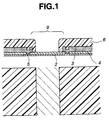
- FIG. 1 is a schematic diagram illustrating the surrounding structure of an ink-jet head according to a first embodiment of the present invention.
- the present invention provides the configuration of a protective layer which can assuredly cover electrothermal transducers even if the thickness of the layer is small. That is, a thin intermediate layer is provided between a heating resistive layer and electrodes, and the thin intermediate layer on heating portions comprises an insulator. According to this configuration, the life of the heating resistive layer is increased, and occurrence of burnt deposits is suppressed. Since steps at portions where the thin intermediate layer is provided are small, an excellent film quality is obtained even if the thickness of the layer is small, and therefore an excellent protective property is obtained.
- reference numeral 2 represents a heating resistive layer for generating thermal energy utilized for discharging ink.
- Reference numeral 3 represents interconnection conductors, serving as electrodes, provided on the heating resistive layer 2 and electrically connected thereto, for passing current through the heating resistive layer 2.
- Reference numeral 9 represents a heating portion where the interconnection conductor 3 is not provided on the heating resistive layer 2. Thermal energy is generated from the heating portion 9.
- An thin intermediate layer 4 is provided between the heating resistive layer 2 and the interconnection conductor 3.
- Si 3 N 4 is used for the thin intermediate layer 4.
- the portion of the thin intermediate layer 4 present on the heating portion 9 is an insulator.
- the thin intermediate layer 4 covers the heating portion 9 and contacts both of the heating resistive layer 2 and the interconnection conductors 3. Hence, if the portion of the thin intermediate layer 4 present on the heating portion 9 is a conductor, current flows through the thin intermediate layer 4, and therefore the heating portion 9 does not operate.
- the thin intermediate layer 4 may comprise an insulator, or a metal or the like whose portion on the heating portion 9 is processed to be an insulator. When using an insulator for the thin intermediate layer 4, it is necessary to provide throughholes 5 for electrically connecting the heating resistive layer 2 to the interconnection conductors 3.
- any insulating or metallic materials having cavitation-resistive property may be used for the thin intermediate layer 4.
- insulators such as Si 3 N 4 and SiC
- metals such as Ta and Fe
- the thin intermediate layer 4 Since the thin intermediate layer 4 is proived on the heating resistive layer 2, it can be formed in a state in which substantially no steps are produced. Accordingly, a layer having an excellent film property can be formed even if the thickness of the layer is small.
- the thickness of the thin intermediate layer 4 is preferably 200 - 700 nm.
- a metal for the thin intermediate layer 4 it is preferable to perform heat treatment in an oxygen or nitrogen atmosphere for making a portion on the heating portion 9 an insulator. That is, particularly when using Al for the electrodes 3, the growth of an oxide or nitride layer is prevented by Al 2 O 3 or AlN formed on Al by the heat treatment, and nitriding or oxidation stops at a thickness of about 100 nm. On the other hand, the portion of the thin intermediate layer 4 on the heating portion 9 is completely subjected to nitriding or oxidized. Accordingly, by performing insulating processing by heat treatment in an oxygen or nitrogen atmosphere, a conductive portion having a substantially constant thickness can be obtained in an electrode portion even if the time period of the heat treatment is not controlled. It is, of course, possible to perform insulating processing according to anodic oxidation or the like by controlling the time period of the insulating processing.
- a protective layer 6 is provided on the interconnection conductors 3.
- the protective layer 6 is formed, for example, by coating an organic resin. At that time, the protective layer 6 is provided except on the heating portion 9.
- a Ta/Ir layer having a thickness of 100 nm was formed on a Si substrate 1 having a thermally oxidized film, serving as a heat storage layer, by sputtering.
- the formed layer was etched to a desired pattern, as shown in FIG. 1, to form the heating resistive layer 2.
- a Si 3 N 4 film, serving as the thin intermediate layer 4, having a thickness of 300 nm was formed on the heating resistive layer 2 by sputtering, and throughholes 5 for electrically connecting the interconnection conductors 3, serving as the electrodes, to the heating resistive layer 2 were formed by etching.
- an Al film having a thickness of 500 nm was formed on the thin intermediate layer 4 by sputtering.
- the formed layer was etched to a desired pattern, as shown in FIG. 1, to form the interconnection conductors 3.
- the protective layer 6 was formed by coating Photoneece (trade name: made by Toray Industries, Inc.), serving as an organic resin, on the interconnection conductor 3 to a thickness of 1 ⁇ m followed by provisional curing at 80 - 90 °C, patterning the cured film to a desired shape, and performing complete curing of the film at 350 - 450 °C.
- Photoneece trade name: made by Toray Industries, Inc.
- a top plate having recesses for an ink channel and an ink chamber was connected onto the ink-jet-head substrate obtained in the above-described manner, and thus the ink-jet head of the present embodiment was obtained.
- the heating resistive layer 2 is provided also under the interconnection conductor 3, serving as the electrodes.
- a heating resistive layer is provided only at portions which serve as heating portions.
- FIGS. 2(A) and 2(B) are schematic diagrams illustrating a substrate for an ink-jet head according to the second embodiment.
- the ink-jet head is formed as in the first embodiment except that the pattern of the heating resistive layer is changed as shown in FIGS. 2(A) and 2(B).
- a thin intermediate layer may be provided only on a heating portion, as shown in FIG. 2(B). In this case, it is unnecessary to provide throughholes.
- a thin intermediate layer 4 comprises two layers made of an insulator and a metal, according to a third embodiment of the present invention.
- FIG. 3 is a schematic diagram illustrating the ink-jet head according to the third embodiment.
- a HfB 2 film having a thickness of 100 nm was formed on an Si substrate 1 having a thermally oxided film, serving as a heat storage layer, by sputtering.
- the formed film was etched to a desired pattern, as shown in FIG. 3, to form a heating resistive layer 2.
- a Si 3 N 4 film having a thickness of 300 nm was formed on the heating resistive layer 2 by sputtering as a first thin intermediate layer 4a. Then, throughholes 5 for electrically connecting the interconnection conductors 3, serving as electrodes, to the heating resistive layer 2 were formed by etching.
- a Ta film having a thickness of 200 nm was formed on the Si 3 N 4 layer 4a by sputtering, and portions in the vicinity of boundaries between the formed film and the interconnection conductors 3, and portions between the patterns of the heating resistive layer 2 were etched, to form a second thin intermediate layer 4b.
- an Al film having a thickness of 500 nm was formed on the second thin intermediate layer 4b by sputtering.
- the formed film was etched to a desired pattern, as shown in FIG. 3, to form the interconnection conductors 3.
- a protective layer 6 made of an organic resin was coated on the interconnection conductors 3 to a thickness of 1 ⁇ m, and the organic resin present on the heating portions was removed.
- a top plate having recesses for an ink channel and an ink chamber was connected onto the ink-jet-head substrate obtained in the above-described manner, and thus the ink-jet head of the present embodiment was obtained.
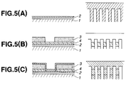
- FIG. 4 is a schematic diagram illustrating a substrate for an ink-jet head according to the fourth embodiment.
- FIGS. 5(A) through 5(C) are diagrams illustrating production processes of the substrate for an ink-jet head according to the fourth embodiment.
- a Ta/Ir film having a thickness of 100 nm was formed on a Si substrate 1 having a thermally oxided film, serving as a heat storage layer, by sputtering.
- the formed film was etched to a desired pattern to form a heating resistive layer 2 (FIG. 5(A)).
- a Ta film having a thickness of 200 nm was formed on the heating resistive layer 2 by sputtering, to form a thin intermediate layer 4.
- the substrate was left in the atmosphere at 500 °C for 10 - 30 hours.
- the surface of the Ta film between the patterns of the interconnection conductors 3 on the heating portions 9 and the surface of the Al film were oxidized to form oxide films (FIG. 5(C)).
- the Ta film serving as the thin intermediate layer 4, is completely converted into a Ta 2 O 5 film.
- the oxidation stops when the thickness of the Al film becomes about 100 nm.
- the Ta film between the patterns of the interconnection conductors 3 on the heating portions 9 is oxidized.
- the Ta/Ir film of the heating resistive layer 2 is not dissolved even if it is immersed in ink.
- a top plate having recesses for an ink channel and an ink chamber was connected onto the ink-jet-head substrate obtained in the above-described manner, and thus the ink-jet head of the present embodiment was obtained.
- An ink-jet head was manufactured in the same manner as in the fourth embodiment except that the heating resistive layer and the thin intermediate layer were changed from the Ta/Ir film and the Ta film to a HfB 2 film and a Fe film, respectively, and insulating processing was performed in a nitrogen atomsphere.
- FIG. 6 is an external perspective view illustrating an example of an ink-jet apparatus (IJA) which mounts an ink-jet head obtained according to the present invention as an ink-jet-head cartridge (IJC).
- IJA ink-jet apparatus
- reference number 20 represents an ink-jet-head cartridge including nozzles for discharging ink while facing a printing surface of printing paper, serving as a printing medium, fed onto a platen 24.
- Reference numeral 16 represents a carriage 16 for holding the IJC 20.
- the carriage 16 is connected to a part of a driving belt 18 for transmitting the driving force of a driving motor 17, and is slidable along two guide shafts 19A and 19B disposed in parallel with each other. Hence, the IJC 20 can reciprocate over the entire width of the printing paper.
- a head recovery device 26 is disposed at one end of a moving path of the IJC 20, for example, at a position facing a home position. Capping of the IJC 20 is performed by the driving force of a motor 22 via a transmission mechanism 23. By performing capping when, for example, terminating printing, the IJC 20 is protected.
- the blade 30 is held by a blade holding member 30A in the form of a cantilever, and operates by the motor 22 and the transmission mechanism 23, as the head recovery device 26, so as to be engageable with a discharging surface of the IJC 20.
- the blade 30 is protruded in the moving path of the IJC 20. Dew condensation, wetting, dust or the like on the discharging surface of the IJC 20 is wiped in accordance with the moving operation of the IJC 20.
- a substrate for an ink-jet head provides a protective layer which can assuredly cover electrothermal transducers even if the thickness of the layer is small.
- a thin intermediate layer is provided between a heating resistive layer and electrodes.
- the thin intermediate layer is an insulator on heating portions of the heating resistive layer. According to such a configuration, the life of the heating resistive layer becomes long, and occurrence of burnt deposits is suppressed. Since steps at portions where the thin intermediate layer is provided are small, an excellent film quality can be obtained even if the thickness of the protective layer is relatively small, and an excellent protective property is obtained.
Applications Claiming Priority (6)
| Application Number | Priority Date | Filing Date | Title |
|---|---|---|---|
| JP7086695 | 1995-03-03 | ||
| JP7086695 | 1995-03-03 | ||
| JP70866/95 | 1995-03-03 | ||
| JP7239195 | 1995-03-06 | ||
| JP7239195 | 1995-03-06 | ||
| JP72391/95 | 1995-03-06 |
Publications (3)
| Publication Number | Publication Date |
|---|---|
| EP0729834A2 true EP0729834A2 (fr) | 1996-09-04 |
| EP0729834A3 EP0729834A3 (fr) | 1997-05-21 |
| EP0729834B1 EP0729834B1 (fr) | 2002-06-12 |
Family
ID=26411992
Family Applications (1)
| Application Number | Title | Priority Date | Filing Date |
|---|---|---|---|
| EP19960103179 Expired - Lifetime EP0729834B1 (fr) | 1995-03-03 | 1996-03-01 | Tête à jet d'encre, couche de base pour tête à jet d'encre et appareil à jet d'encre |
Country Status (2)
| Country | Link |
|---|---|
| EP (1) | EP0729834B1 (fr) |
| DE (1) | DE69621665T2 (fr) |
Cited By (7)
| Publication number | Priority date | Publication date | Assignee | Title |
|---|---|---|---|---|
| EP0951999A3 (fr) * | 1998-04-22 | 2000-05-03 | Hewlett-Packard Company | Tête d'impression à jet d'encre adaptée pour la réduction du volume des gouttes d'encre |
| US6331049B1 (en) | 1999-03-12 | 2001-12-18 | Hewlett-Packard Company | Printhead having varied thickness passivation layer and method of making same |
| WO2002083424A1 (fr) * | 2001-04-13 | 2002-10-24 | Sony Corporation | Tete d'injection de liquide, dispositif d'injection de liquide et procede de fabrication d'une tete d'injection de liquide |
| US7025894B2 (en) | 2001-10-16 | 2006-04-11 | Hewlett-Packard Development Company, L.P. | Fluid-ejection devices and a deposition method for layers thereof |
| EP1968797A2 (fr) * | 2005-12-23 | 2008-09-17 | Lexmark International, Inc., Intellectual Property Law Dept. | Dispositif d ejection de microfluide a faible consommation d energie et a longue duree de vie |
| CN101125482B (zh) * | 2001-10-30 | 2010-04-21 | 佳能株式会社 | 具有贯通孔的结构体、其制造方法及液体排出头 |
| US7838155B2 (en) | 2001-03-13 | 2010-11-23 | Sony Corporation | Aqueous electrolyte solution absorber and method for producing it |
Citations (6)
| Publication number | Priority date | Publication date | Assignee | Title |
|---|---|---|---|---|
| JPS5582677A (en) * | 1978-12-18 | 1980-06-21 | Toshiba Corp | Thermal head |
| JPS5582678A (en) * | 1978-12-19 | 1980-06-21 | Toshiba Corp | Thermal head |
| JPS62202754A (ja) * | 1986-03-03 | 1987-09-07 | Tdk Corp | 薄膜型サ−マルヘツド |
| US4951063A (en) * | 1989-05-22 | 1990-08-21 | Xerox Corporation | Heating elements for thermal ink jet devices |
| EP0396315A1 (fr) * | 1989-05-01 | 1990-11-07 | Xerox Corporation | Tête d'impression thermique à jet d'encre avec des éléments chauffants générant des bulles |
| EP0596705A2 (fr) * | 1992-11-05 | 1994-05-11 | Xerox Corporation | Elément chauffant pour tête d'impression thermique par jet d'encre |
-
1996
- 1996-03-01 EP EP19960103179 patent/EP0729834B1/fr not_active Expired - Lifetime
- 1996-03-01 DE DE1996621665 patent/DE69621665T2/de not_active Expired - Lifetime
Patent Citations (6)
| Publication number | Priority date | Publication date | Assignee | Title |
|---|---|---|---|---|
| JPS5582677A (en) * | 1978-12-18 | 1980-06-21 | Toshiba Corp | Thermal head |
| JPS5582678A (en) * | 1978-12-19 | 1980-06-21 | Toshiba Corp | Thermal head |
| JPS62202754A (ja) * | 1986-03-03 | 1987-09-07 | Tdk Corp | 薄膜型サ−マルヘツド |
| EP0396315A1 (fr) * | 1989-05-01 | 1990-11-07 | Xerox Corporation | Tête d'impression thermique à jet d'encre avec des éléments chauffants générant des bulles |
| US4951063A (en) * | 1989-05-22 | 1990-08-21 | Xerox Corporation | Heating elements for thermal ink jet devices |
| EP0596705A2 (fr) * | 1992-11-05 | 1994-05-11 | Xerox Corporation | Elément chauffant pour tête d'impression thermique par jet d'encre |
Non-Patent Citations (3)
| Title |
|---|
| PATENT ABSTRACTS OF JAPAN vol. 004, no. 125 (M-030), 3 September 1980 & JP 55 082677 A (TOSHIBA CORP), 21 June 1980, * |
| PATENT ABSTRACTS OF JAPAN vol. 004, no. 125 (M-030), 3 September 1980 & JP 55 082678 A (TOSHIBA CORP), 21 June 1980, * |
| PATENT ABSTRACTS OF JAPAN vol. 012, no. 055 (M-669), 19 February 1988 & JP 62 202754 A (TDK CORP), 7 September 1987, * |
Cited By (14)
| Publication number | Priority date | Publication date | Assignee | Title |
|---|---|---|---|---|
| EP0951999A3 (fr) * | 1998-04-22 | 2000-05-03 | Hewlett-Packard Company | Tête d'impression à jet d'encre adaptée pour la réduction du volume des gouttes d'encre |
| US6293654B1 (en) | 1998-04-22 | 2001-09-25 | Hewlett-Packard Company | Printhead apparatus |
| KR100440109B1 (ko) * | 1998-04-22 | 2004-07-15 | 휴렛-팩커드 컴퍼니(델라웨어주법인) | 잉크젯 프린트 헤드 장치 |
| US6331049B1 (en) | 1999-03-12 | 2001-12-18 | Hewlett-Packard Company | Printhead having varied thickness passivation layer and method of making same |
| US7838155B2 (en) | 2001-03-13 | 2010-11-23 | Sony Corporation | Aqueous electrolyte solution absorber and method for producing it |
| US7182440B2 (en) | 2001-04-13 | 2007-02-27 | Sony Corporation | Liquid jet apparatus |
| KR100866270B1 (ko) * | 2001-04-13 | 2008-11-03 | 소니 가부시끼 가이샤 | 액체 분사 헤드, 액체 분사 장치 및 액체 분사 헤드의제조 방법 |
| US7836598B2 (en) | 2001-04-13 | 2010-11-23 | Sony Corporation | Method of manufacturing a thermal liquid jet head using an etching process |
| WO2002083424A1 (fr) * | 2001-04-13 | 2002-10-24 | Sony Corporation | Tete d'injection de liquide, dispositif d'injection de liquide et procede de fabrication d'une tete d'injection de liquide |
| US7025894B2 (en) | 2001-10-16 | 2006-04-11 | Hewlett-Packard Development Company, L.P. | Fluid-ejection devices and a deposition method for layers thereof |
| US7517060B2 (en) | 2001-10-16 | 2009-04-14 | Hewlett-Packard Development Company, L.P. | Fluid-ejection devices and a deposition method for layers thereof |
| CN101125482B (zh) * | 2001-10-30 | 2010-04-21 | 佳能株式会社 | 具有贯通孔的结构体、其制造方法及液体排出头 |
| EP1968797A2 (fr) * | 2005-12-23 | 2008-09-17 | Lexmark International, Inc., Intellectual Property Law Dept. | Dispositif d ejection de microfluide a faible consommation d energie et a longue duree de vie |
| EP1968797A4 (fr) * | 2005-12-23 | 2010-08-11 | Lexmark International Inc Inte | Dispositif d ejection de microfluide a faible consommation d energie et a longue duree de vie |
Also Published As
| Publication number | Publication date |
|---|---|
| DE69621665T2 (de) | 2003-03-06 |
| EP0729834B1 (fr) | 2002-06-12 |
| DE69621665D1 (de) | 2002-07-18 |
| EP0729834A3 (fr) | 1997-05-21 |
Similar Documents
| Publication | Publication Date | Title |
|---|---|---|
| US20040032466A1 (en) | Method for producing organic insulating coating and ink-jet printhead produced according to the method | |
| WO2001074592A1 (fr) | Tete a jet d'encre a buses multiples et son procede de fabrication | |
| EP1717036B1 (fr) | Procédé de fabrication de plaque à buses d'éjection pour tête d'impression à jet d'encre | |
| WO2001074591A1 (fr) | Tete a jet d'encre a buses multiples | |
| EP0729834A2 (fr) | Tête à jet d'encre, couche de base pour tête à jet d'encre et appareil à jet d'encre | |
| EP0539993B1 (fr) | Tête d'impression à jet d'encre et son procédé de fabrication | |
| KR19990023939A (ko) | 잉크-젯 프린트헤드와 그 제조 방법 | |
| US5612724A (en) | Ink jet recording head with enhanced bonding force between a heat storing layer and substrate, a method of forming the same and a recording apparatus having said recording head | |
| JP3402618B2 (ja) | インクジェット記録ヘッドの製造方法および記録装置 | |
| EP0885723B1 (fr) | Unité d'éléments d'enregistrement, unité d'éléments d'enregistrement à jet d'encre, cartouche à jet d'encre et appareil d'enregistrement à jet d'encre | |
| JP4078295B2 (ja) | インクジェットヘッド用基体およびこれを用いるインクジェットヘッドとその製造方法 | |
| US6352338B1 (en) | Ink-jet print head, production method thereof, and printing apparatus with the ink-jet print head | |
| KR100828362B1 (ko) | 잉크젯 프린트헤드용 히터 및 이 히터를 구비하는 잉크젯프린트헤드 | |
| JP2933429B2 (ja) | 液体噴射記録ヘッド用基板、液体噴射記録ヘッドおよび液体噴射記録装置 | |
| JP3454490B2 (ja) | インクジェットヘッド、インクジェットヘッド用基板及びインクジェット装置 | |
| JP3563960B2 (ja) | インクジェットヘッド用基体、インクジェットヘッド、インクジェット装置およびインクジェットヘッド用基体の製造方法 | |
| JP2727989B2 (ja) | サーマルヘッドの製造方法 | |
| JP2002011886A (ja) | インクジェット記録ヘッド用基板、インクジェット記録ヘッド、および該ヘッド用基板の作成方法 | |
| JP3149316B2 (ja) | サーマルヘッドおよびその製造方法 | |
| JPH07125208A (ja) | インクジェットヘッドおよびインクジェット記録装置 | |
| JP3061935B2 (ja) | インクジェット記録ヘッド及びインクジェット記録装置の製造方法 | |
| JP2000006414A (ja) | インクジェット記録ヘッド及び該ヘッドを用いたインクジェット記録装置 | |
| JP2000006411A (ja) | インクジェット記録素子及びこれを用いたインクジェット記録装置 | |
| JPH0577415A (ja) | インクジエツトヘツド | |
| JP2007180249A (ja) | アクチュエータ装置の製造方法及び液体噴射装置 |
Legal Events
| Date | Code | Title | Description |
|---|---|---|---|
| PUAI | Public reference made under article 153(3) epc to a published international application that has entered the european phase |
Free format text: ORIGINAL CODE: 0009012 |
|
| AK | Designated contracting states |
Kind code of ref document: A2 Designated state(s): DE FR GB IT |
|
| PUAL | Search report despatched |
Free format text: ORIGINAL CODE: 0009013 |
|
| AK | Designated contracting states |
Kind code of ref document: A3 Designated state(s): DE FR GB IT |
|
| 17P | Request for examination filed |
Effective date: 19971007 |
|
| 17Q | First examination report despatched |
Effective date: 19990521 |
|
| GRAG | Despatch of communication of intention to grant |
Free format text: ORIGINAL CODE: EPIDOS AGRA |
|
| GRAG | Despatch of communication of intention to grant |
Free format text: ORIGINAL CODE: EPIDOS AGRA |
|
| GRAH | Despatch of communication of intention to grant a patent |
Free format text: ORIGINAL CODE: EPIDOS IGRA |
|
| GRAH | Despatch of communication of intention to grant a patent |
Free format text: ORIGINAL CODE: EPIDOS IGRA |
|
| GRAA | (expected) grant |
Free format text: ORIGINAL CODE: 0009210 |
|
| AK | Designated contracting states |
Kind code of ref document: B1 Designated state(s): DE FR GB IT |
|
| REG | Reference to a national code |
Ref country code: GB Ref legal event code: FG4D |
|
| REF | Corresponds to: |
Ref document number: 69621665 Country of ref document: DE Date of ref document: 20020718 |
|
| ET | Fr: translation filed | ||
| PLBE | No opposition filed within time limit |
Free format text: ORIGINAL CODE: 0009261 |
|
| STAA | Information on the status of an ep patent application or granted ep patent |
Free format text: STATUS: NO OPPOSITION FILED WITHIN TIME LIMIT |
|
| 26N | No opposition filed |
Effective date: 20030313 |
|
| PGFP | Annual fee paid to national office [announced via postgrant information from national office to epo] |
Ref country code: DE Payment date: 20140331 Year of fee payment: 19 |
|
| PGFP | Annual fee paid to national office [announced via postgrant information from national office to epo] |
Ref country code: IT Payment date: 20140304 Year of fee payment: 19 |
|
| PGFP | Annual fee paid to national office [announced via postgrant information from national office to epo] |
Ref country code: GB Payment date: 20140318 Year of fee payment: 19 |
|
| PGFP | Annual fee paid to national office [announced via postgrant information from national office to epo] |
Ref country code: FR Payment date: 20140326 Year of fee payment: 19 |
|
| REG | Reference to a national code |
Ref country code: DE Ref legal event code: R119 Ref document number: 69621665 Country of ref document: DE |
|
| GBPC | Gb: european patent ceased through non-payment of renewal fee |
Effective date: 20150301 |
|
| PG25 | Lapsed in a contracting state [announced via postgrant information from national office to epo] |
Ref country code: IT Free format text: LAPSE BECAUSE OF NON-PAYMENT OF DUE FEES Effective date: 20150301 |
|
| REG | Reference to a national code |
Ref country code: FR Ref legal event code: ST Effective date: 20151130 |
|
| PG25 | Lapsed in a contracting state [announced via postgrant information from national office to epo] |
Ref country code: DE Free format text: LAPSE BECAUSE OF NON-PAYMENT OF DUE FEES Effective date: 20151001 Ref country code: GB Free format text: LAPSE BECAUSE OF NON-PAYMENT OF DUE FEES Effective date: 20150301 |
|
| PG25 | Lapsed in a contracting state [announced via postgrant information from national office to epo] |
Ref country code: FR Free format text: LAPSE BECAUSE OF NON-PAYMENT OF DUE FEES Effective date: 20150331 |