EP0729129B1 - Anzeigesystem und -verfahren mit einer Bildumwandlung, die ohne visuelle Inspektion kontrolliert werden kann - Google Patents
Anzeigesystem und -verfahren mit einer Bildumwandlung, die ohne visuelle Inspektion kontrolliert werden kann Download PDFInfo
- Publication number
- EP0729129B1 EP0729129B1 EP96102531A EP96102531A EP0729129B1 EP 0729129 B1 EP0729129 B1 EP 0729129B1 EP 96102531 A EP96102531 A EP 96102531A EP 96102531 A EP96102531 A EP 96102531A EP 0729129 B1 EP0729129 B1 EP 0729129B1
- Authority
- EP
- European Patent Office
- Prior art keywords
- display
- data
- flcd
- image
- line
- Prior art date
- Legal status (The legal status is an assumption and is not a legal conclusion. Google has not performed a legal analysis and makes no representation as to the accuracy of the status listed.)
- Expired - Lifetime
Links
- 238000000034 method Methods 0.000 title claims description 12
- 238000006243 chemical reaction Methods 0.000 title claims description 10
- 238000012545 processing Methods 0.000 title description 64
- 230000000007 visual effect Effects 0.000 title description 3
- 238000012546 transfer Methods 0.000 claims description 64
- 230000010365 information processing Effects 0.000 claims description 33
- 239000005262 ferroelectric liquid crystals (FLCs) Substances 0.000 claims description 11
- 238000003860 storage Methods 0.000 claims description 2
- 230000014759 maintenance of location Effects 0.000 claims 1
- 238000010586 diagram Methods 0.000 description 10
- 238000009792 diffusion process Methods 0.000 description 10
- 239000003086 colorant Substances 0.000 description 9
- 239000004973 liquid crystal related substance Substances 0.000 description 8
- 238000012360 testing method Methods 0.000 description 8
- 230000006870 function Effects 0.000 description 7
- 238000001514 detection method Methods 0.000 description 6
- 239000000872 buffer Substances 0.000 description 5
- 230000008859 change Effects 0.000 description 4
- 230000002159 abnormal effect Effects 0.000 description 3
- 210000002858 crystal cell Anatomy 0.000 description 3
- 230000008901 benefit Effects 0.000 description 2
- 238000004040 coloring Methods 0.000 description 2
- 230000005684 electric field Effects 0.000 description 2
- 239000011159 matrix material Substances 0.000 description 2
- 238000012986 modification Methods 0.000 description 2
- 230000004048 modification Effects 0.000 description 2
- 230000004044 response Effects 0.000 description 2
- 230000003213 activating effect Effects 0.000 description 1
- 230000007175 bidirectional communication Effects 0.000 description 1
- 210000004027 cell Anatomy 0.000 description 1
- 230000006854 communication Effects 0.000 description 1
- 238000004891 communication Methods 0.000 description 1
- 230000002950 deficient Effects 0.000 description 1
- 238000002405 diagnostic procedure Methods 0.000 description 1
- 238000009826 distribution Methods 0.000 description 1
- 239000000284 extract Substances 0.000 description 1
- 238000004519 manufacturing process Methods 0.000 description 1
- 230000003446 memory effect Effects 0.000 description 1
- 238000012544 monitoring process Methods 0.000 description 1
- 230000008569 process Effects 0.000 description 1
- 239000010453 quartz Substances 0.000 description 1
- 230000005855 radiation Effects 0.000 description 1
- 230000009467 reduction Effects 0.000 description 1
- 238000005070 sampling Methods 0.000 description 1
- VYPSYNLAJGMNEJ-UHFFFAOYSA-N silicon dioxide Inorganic materials O=[Si]=O VYPSYNLAJGMNEJ-UHFFFAOYSA-N 0.000 description 1
- 229910000679 solder Inorganic materials 0.000 description 1
Images


Classifications
-
- G—PHYSICS
- G09—EDUCATION; CRYPTOGRAPHY; DISPLAY; ADVERTISING; SEALS
- G09G—ARRANGEMENTS OR CIRCUITS FOR CONTROL OF INDICATING DEVICES USING STATIC MEANS TO PRESENT VARIABLE INFORMATION
- G09G3/00—Control arrangements or circuits, of interest only in connection with visual indicators other than cathode-ray tubes
- G09G3/006—Electronic inspection or testing of displays and display drivers, e.g. of LED or LCD displays
-
- G—PHYSICS
- G09—EDUCATION; CRYPTOGRAPHY; DISPLAY; ADVERTISING; SEALS
- G09G—ARRANGEMENTS OR CIRCUITS FOR CONTROL OF INDICATING DEVICES USING STATIC MEANS TO PRESENT VARIABLE INFORMATION
- G09G5/00—Control arrangements or circuits for visual indicators common to cathode-ray tube indicators and other visual indicators
-
- G—PHYSICS
- G09—EDUCATION; CRYPTOGRAPHY; DISPLAY; ADVERTISING; SEALS
- G09G—ARRANGEMENTS OR CIRCUITS FOR CONTROL OF INDICATING DEVICES USING STATIC MEANS TO PRESENT VARIABLE INFORMATION
- G09G3/00—Control arrangements or circuits, of interest only in connection with visual indicators other than cathode-ray tubes
- G09G3/20—Control arrangements or circuits, of interest only in connection with visual indicators other than cathode-ray tubes for presentation of an assembly of a number of characters, e.g. a page, by composing the assembly by combination of individual elements arranged in a matrix no fixed position being assigned to or needed to be assigned to the individual characters or partial characters
- G09G3/34—Control arrangements or circuits, of interest only in connection with visual indicators other than cathode-ray tubes for presentation of an assembly of a number of characters, e.g. a page, by composing the assembly by combination of individual elements arranged in a matrix no fixed position being assigned to or needed to be assigned to the individual characters or partial characters by control of light from an independent source
- G09G3/36—Control arrangements or circuits, of interest only in connection with visual indicators other than cathode-ray tubes for presentation of an assembly of a number of characters, e.g. a page, by composing the assembly by combination of individual elements arranged in a matrix no fixed position being assigned to or needed to be assigned to the individual characters or partial characters by control of light from an independent source using liquid crystals
- G09G3/3611—Control of matrices with row and column drivers
- G09G3/3622—Control of matrices with row and column drivers using a passive matrix
- G09G3/3629—Control of matrices with row and column drivers using a passive matrix using liquid crystals having memory effects, e.g. ferroelectric liquid crystals
-
- G—PHYSICS
- G09—EDUCATION; CRYPTOGRAPHY; DISPLAY; ADVERTISING; SEALS
- G09G—ARRANGEMENTS OR CIRCUITS FOR CONTROL OF INDICATING DEVICES USING STATIC MEANS TO PRESENT VARIABLE INFORMATION
- G09G2310/00—Command of the display device
- G09G2310/04—Partial updating of the display screen
-
- G—PHYSICS
- G09—EDUCATION; CRYPTOGRAPHY; DISPLAY; ADVERTISING; SEALS
- G09G—ARRANGEMENTS OR CIRCUITS FOR CONTROL OF INDICATING DEVICES USING STATIC MEANS TO PRESENT VARIABLE INFORMATION
- G09G2360/00—Aspects of the architecture of display systems
- G09G2360/02—Graphics controller able to handle multiple formats, e.g. input or output formats
-
- G—PHYSICS
- G09—EDUCATION; CRYPTOGRAPHY; DISPLAY; ADVERTISING; SEALS
- G09G—ARRANGEMENTS OR CIRCUITS FOR CONTROL OF INDICATING DEVICES USING STATIC MEANS TO PRESENT VARIABLE INFORMATION
- G09G2370/00—Aspects of data communication
- G09G2370/04—Exchange of auxiliary data, i.e. other than image data, between monitor and graphics controller
- G09G2370/045—Exchange of auxiliary data, i.e. other than image data, between monitor and graphics controller using multiple communication channels, e.g. parallel and serial
-
- G—PHYSICS
- G09—EDUCATION; CRYPTOGRAPHY; DISPLAY; ADVERTISING; SEALS
- G09G—ARRANGEMENTS OR CIRCUITS FOR CONTROL OF INDICATING DEVICES USING STATIC MEANS TO PRESENT VARIABLE INFORMATION
- G09G3/00—Control arrangements or circuits, of interest only in connection with visual indicators other than cathode-ray tubes
- G09G3/20—Control arrangements or circuits, of interest only in connection with visual indicators other than cathode-ray tubes for presentation of an assembly of a number of characters, e.g. a page, by composing the assembly by combination of individual elements arranged in a matrix no fixed position being assigned to or needed to be assigned to the individual characters or partial characters
- G09G3/2007—Display of intermediate tones
- G09G3/2059—Display of intermediate tones using error diffusion
Definitions
- the present invention relates to a method and an apparatus for performing control of a display.
- a display device In an information processing system (or apparatus), a display device is generally used as a means for realizing an information visual expression function.
- a CRT display device is most popular as such a display device, as is well known.
- an operation for writing an image to be displayed in a video memory (to be referred to as a VRAM hereinafter) arranged in an information processing apparatus and an operation for reading out display data from the VRAM are independently performed.
- the number of display dots on a display device in an information processing apparatus is generally 640 x 400 to 640 x 480 dots.
- the number of display colors is a maximum of 16 in most display devices.
- the display board or card is a so-called graphic accelerator board (card) (to be referred to as a display control board hereinafter).
- LCD liquid crystal display
- the number of colors is generally smaller than that of the CRT. Therefore, image data to be displayed on the LCD must be processed to some extent, and the processing result must be displayed.
- the present applicant has proposed a display using a ferroelectric liquid crystal cell (this display will be referred to as an FLCD hereinafter) as one of the LCDs.
- an FLCD ferroelectric liquid crystal cell
- One of the features of the FLCD lies in that a liquid crystal cell can retain its display state with respect to application of an electric field. More specifically, the FLCD has a sufficiently thin liquid crystal cell, and each elongated FLC element in the cell maintains its aligned state even upon removal of the applied electric field.
- the FLCD using this FLC element has a memory effect for storing display contents due to the bistable properties of the FLC element.
- the details of the FLC and FLCD are described in U.S. Patent No. 4,964,699.
- the number of colors of the FLCD is 16 at present. However, binarization such as error diffusion can greatly increase the apparent number of display colors.
- this FLCD is, of course, one confirmed to operate properly
- a sample image is displayed, and it is determined by observation with the human eye whether a defective portion is present. This operation is time-consuming and requires much labor of those who test the graphic accelerator boards.
- binarization halftone processing is performed to increase the number of pseudo display colors.
- a typical example is an ED (Error Diffusion) method for maintaining the image qualities of both a natural image and a character image. This ED processing requires continuity of an image in processing because an error occurring in a given pixel is sequentially diffused (distributed) to adjacent pixels.
- an error occurring in the process propagates like a wave, so that an image as a processing target must be continuous. If some updated portions are present, these portions become discrete in the vertical direction.
- the transfer rate of the ED processing result must be equal to that of the FLCD.
- the partial rewrite position is not fixed, but may be an arbitrary position on the display screen. To cope with this by directly transferring the ED processing result to the FLCD, some technical problems are left unsolved.
- the EP 0 572 143 A discloses a display control apparatus and method.
- Frame buffers are shown, which store data supplied from a CPU.
- the data from the frame buffers are supplied to a binarizing image processing circuit 34 and to a coloring circuit 36.
- the image data converted by the binarizing image processing circuit or coloring circuit are supplied to frame buffers 301 and 302.
- the US 5 055 928 discloses a digital video frame recorder with a video display test pattern signal generator.
- the frame recorder comprises a frame memory for storing data to be output by an output processor as output video signal.
- a memory and system controller controls the basic functions of the frame recorder. It further controls a self-diagnostic testing performed by a microprocessor. According to its preprogrammed instructions or user commands, the microprocessor transfers preprogrammed test data to a FIFO register. This test data is written into and back out from the frame memory and back into the FIFO register. By comparing this test data returning from the frame memory with the original test data, the microprocessor determines whether the frame memory is functioning properly.
- this object is achieved by an apparatus according to claim 1 and by a method according to claim 8.
- the image transferred from the second memory means to the display can be located at an arbitrary position, and a display image in the transferred image does not become unnatural.
- the apparatus of the present invention is not limited to use with a dedicated information processing apparatus but can be used together with a general-purpose information processing apparatus.
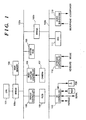
- reference numeral 101 denotes a CPU for controlling the overall information processing system
- 102a a bus (e.g., a PCI bus) which can perform high-speed transfer and includes an address bus, a control bus, and a data bus
- 102b a middle-speed bus for performing data transfer, which is not faster than that of the bus 102a
- 103 a system ROM storing a boot program, a BIOS, and the like.
- Reference numeral 104 denotes a main memory consisting of a RAM in which the OS and various application programs are loaded.
- Reference numerals 105a and 105b denote bridges for performing arbitration between different buses.
- Reference numeral 106 denotes a video capture controller which serves as a circuit to capture a video output from a video camera 107 or the like to the apparatus.
- Reference numeral 108 denotes a display controller serving as the main part of this embodiment.
- the display controller 108 converts input data into an image to be displayed on an FLCD 109 (the display controller 108 and the FLCD 108 will be described in detail later).
- Reference numeral 110 denotes an audio sub-system for sampling a signal from a sound source such as a microphone and converts it into digital data.
- the audio sub-system 110 also converts digital data into an analog signal which is then output from a loudspeaker.
- Reference numeral 111 denotes a quartz oscillator which serves as a real-time clock having a timepiece function; and 112, a keyboard controller for receiving a key input signal from a keyboard and an input signal from a pointing device and transmits them to the CPU 101.
- Reference numeral 113 denotes an I/O controller which comprises a floppy disk drive (FDD), a hard disk drive (HDD), a serial interface, and a parallel interface, as shown in Fig. 1.
- the I/O controller 113 can connect a general-purpose apparatus.
- the HDD stores the OS (Operating System) and various application programs of the system of this embodiment.
- a display RAM (VRAM) and circuits for processing images stored in the VRAM into data to be displayed on the FLCD 109 are included in the display controller 108.
- the display controller 108 may be permanently connected to the system, or may be connected as a card (or board) mounted in an expansion slot formed in an information processing apparatus generally represented by a workstation or personal computer. More specifically, the FLCD 109 and the display controller 108 of this embodiment may be incorporated in the system in any form, or may be connected as independent external devices. Note that when the FLCD 109 is arranged separately form the information processing apparatus, the FLCD 109 is connected to the display controller 108 through a cable.
- the OS and an application program are loaded in the memory 104 through the I/O controller 113 in the system of this embodiment and are executed. Image information under execution is stored in the VRAM arranged in the display controller 108 and is displayed on the FLCD 109.
- any OS and any application program can be used.
- an MS-WINDOWS available from Microsoft, U.S.A.
- any application program which runs on this OS can be used.
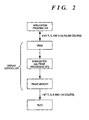
- FIG. 2 The concept of a data flow associated with an image display in the system of this embodiment is shown in Fig. 2.
- the written data is subjected to binarization halftone processing (error diffusion (ED) processing in this embodiment).
- ED error diffusion
- the contents of this frame memory are transferred to the FLCD 109 and displayed.
- the contents of the VRAM are directly transferred to the display device.
- the frame memory is interposed between the VRAM and the FLCD 109 serving as the display in the display controller 108 of this embodiment.
- Fig. 3 is a detailed block diagram of the display controller 108 in this embodiment.
- reference numeral 300 denotes a CPU arranged in the display controller 108 to control the overall display controller. This CPU 300 operates in accordance with programs stored in a ROM 308.
- the VRAM 301 has a capacity which can store an image having a size of 1,280 x 1,024 dots (i.e., 1,280 x 1,024 x 3 ⁇ 4 Mbytes).
- Reference numeral 302 denotes an SVGA for controlling access to the VRAM 301.
- the SVGA 302 can draw (write) data in the VRAM 301 or read out data from the VRAM 301 on the basis of an instruction from the CPU 101 on the information processing system side.
- the SVGA 302 also has a function of drawing a figure or the like on the basis of an instruction from the CPU 101 and other functions to be described later. Note that an LSI for drawing various figures in the VRAM is widely used as a display control chip and is known well.
- Reference numeral 303 denotes a write detection/flag generation circuit.
- a write enable signal (actually including a chip select signal) is used as a trigger pulse to detect the write address, calculates the updated line number, and holds this information.
- the circuit 303 latches the corresponding output address in a register (not shown). The circuit 303 then calculates the number of a line having undergone write access from the latched address data (this can be calculated by a circuit for dividing the write address by the number of bytes of one line). The circuit 303 then sets "1" in the area flag corresponding to the rewritten line.
- the number of lines of the entire screen of the FLCD 109 is 1,024 (0th line to 1023rd line), and each area is set in units of 32 lines.
- a display image change generally concerns not one line but often influences a plurality of lines.
- the number of lines assigned to one area is not limited to 32, but may be any arbitrary number.
- the number of bits of the area flag portion undesirably increases.
- the number of partial rewrite instructions also increases with an increase in the number of bits of the area flag portion, thereby increasing the overhead amount.
- the number of lines assigned to one area is determined to be 32.
- the maximum resolution of the FLCD 109 is 1,280 x 1,024 as will be described in detail later.
- the information volume of one line is programmable so as to calculate the rewrite line number.
- a change in the number of display dots is based on an instruction from the CPU 102 on the information processing apparatus side (the currently running program is the control driver of the display controller in this embodiment).
- the rewrite detection/flag generation circuit 303 When the rewrite detection/flag generation circuit 303 detects that a rewrite operation is performed for an area of 32 lines written in the VRAM 301, the circuit 303 notifies the CPU 300 of the contents of this area flag. As will be described later, the rewrite detection/flag generation circuit 303 also clears the area flag to zero in response to a request from the CPU 300.
- Reference numeral 304 denotes a line address generation circuit for receiving the start address of a line designated from the CPU 300, the number of offset lines from the designated line, and outputting data transfer address and its control signal to the SVGA chip 302.
- the SVGA chip 302 receives this address data and the control signal and outputs image data (R, G, and B each having 8 bits/pixel) of the number of lines designated from the corresponding line to a binarization halftone processing circuit 305 (to be described below).
- the binarization halftone processing circuit 305 quantizes the image data (three 8-bit R, G, and B data per pixel) transferred from the SVGA chip 302 into R, G, and B signals and a intensity signal I (each signal has one bit, that is, a total of four bits) on the basis of an error diffusion method.
- a technique for binarizing an 8-bit R, G, or B signal into a 1-bit R, G, or B signal and generating a binary signal I representing the luminance level has already been proposed by the present applicant (e.g., Japanese Patent Application No. 4-126148 (U.S. Patent Application No. 08/062,337)).
- the binarization halftone processing circuit 305 incorporates a buffer memory required to execute error diffusion processing.
- the binarization halftone processing circuit 305 receives an error diffusion table (parameters), an output line position, and the number of output lines, all of which serve as binarization parameters, on the basis of an instruction from the CPU 300, and outputs data on the basis of these parameters.
- the error diffusion table is not permanent, but can be arbitrarily set under the control of the CPU 300 due to the following reason. For example, the color arrangement or the like can be changed on the basis of an instruction from the CPU 101 on the information processing apparatus side.
- Reference numeral 306 denotes a frame memory for storing an image (three 1-bit R, G, and B data per pixel) to be displayed on the FLCD 109.
- the FLCD 109 of this embodiment has a resolution of 1,280 x 1,024 dots. Each dot has 4 bits, so that the frame memory has a 1-Mbyte (640 Kbytes in the calculation) capacity.
- Reference numeral 307 denotes a frame memory control circuit for controlling write access and read access to the frame memory and transfer of data to the FLCD 109. The details of the frame memory control circuit 307 will be described later.
- the frame memory control circuit 307 stores the R, G, B, and I data output from the binarization halftone processing circuit 305 in the frame memory 306 and outputs the area designated by the CPU 300 to the FLCD 109 (after one-line data is stored in a FIFO memory 307a, the stored data is transferred).
- the frame memory control circuit 307 notifies the CPU 300 of this using an interrupt signal.
- the data format in transfer to the FLCD 109 has a set of four bits, i.e., four 1-bit R, G, B, and I signals, and data is also stored in the frame memory 306 in this data format.
- the frame memory control circuit 307 When storage of the image data from the binarization halftone processing circuit 305 in the frame memory 306 is completed, the frame memory control circuit 307 notifies the CPU 300 of this using an interrupt signal. Similarly, when transfer of image data of the line designated from the CPU 300 is completed (transfer of image data of a plurality of lines is completed upon designation of transfer of the plurality of lines), the frame memory control circuit 307 notifies the CPU 300 of this using an interrupt signal.
- the CPU 101 in the information processing apparatus receives a drawing request for a character or figure from the OS or an application program
- the CPU 101 outputs a drawing command or image data to the SVGA chip 302 in the display controller 108.
- the SVGA chip 302 Upon reception of image data, the SVGA chip 302 writes this image at the designated location in the VRAM 301.
- a drawing command for figure data or the like a figure image is drawn at the corresponding location in the VRAM 301. More specifically, the SVGA chip 302 performs write access to the VRAM 301.
- the rewrite detection/flag generation circuit 303 monitors write access of the SVGA chip 302. As a result, a flag for a written area is set, and the CPU 300 is notified of this operation.
- the CPU 300 reads the area flag stored in the rewrite detection/flag generation circuit 303 and resets this area flag in the rewrite detection/flag generation circuit 303 to prepare for the next rewrite operation. Note that this reset operation may be performed using a hardware means for simultaneously performing the reset operation and the read operation.
- the CPU 300 determines from the read area flag which bit is set, i.e., which area (or areas) has undergone the rewrite operation. To transfer the area determined to be rewritten from the VRAM 301 to the binarization halftone processing circuit 305, the CPU 300 outputs, to the line address generation circuit 304, the start address of the transfer start line (normally the address of the left corner on the screen) and data presenting the number of lines to be transferred from the transfer start line.
- a distance which renders the influence of an error negligible is determined depending on the size and weighting factor values of an error diffusion matrix.
- Error diffusion processing in the binarization halftone processing circuit 305 in this embodiment is performed from the upper left corner to the lower right corner of the image, as may be readily understood from the above description.
- the CPU 300 outputs, to the binarization halftone processing circuit 305, an instruction representing a specific output portion of the line data of the processing result.
- the data of the 315th line to the 351st line is transferred to the binarization halftone processing circuit 305.
- the CPU 300 outputs an instruction to output the data of the 320th line to the 351th line to the binarization halftone processing circuit 305.
- the binarization halftone processing circuit 305 outputs, to the frame memory control circuit 307, the data of the 320th line to the 351th line which have received the influence of the non-changed portion before the 319th line.
- the frame control memory circuit 307 writes data (four bits/pixel) in units of lines output from the binarization halftone processing circuit 305 in the corresponding frame memory 306. More specifically, since the CPU 300 has detected the number of lines output from the binarization halftone processing circuit and the line number of the start line of these lines in the image, the CPU 300 sets the input line address (the write start address for the frame memory 306) and data representing the number of consecutive lines to the frame memory control circuit 307.
- the frame memory 306 stores the rewritten (updated image) portion of the image and a joint portion between the written image and the nonwritten image as a natural image. Note that when data transfer from the binarization halftone processing circuit 305 to the frame memory 306 is completed for the area designated from the CPU 300, the frame memory control circuit 307 generates an interrupt signal as described above.
- the processing speed of the binarization halftone processing circuit 305 in this embodiment is about 1/30 second for a frame at present. This processing speed is about half the frequency (about 60 Hz) of the vertical sync signal as in a CRT. However, the entire frame is rarely rewritten as long as an ordinary application program is used. In other words, the number of lines processed by the binarization halftone processing circuit 305 in practice is not so large. The period until completion of processing is almost equal to the display update period of the CRT with respect to the entire screen because the processing volume is small. If the portion to be rewritten is less than half the entire screen, the processing speed is higher than that of the CRT.
- the frame memory control circuit 307 also receives an output instruction for the FLCD 109 from the CPU 300.
- the output instruction instructs to output the number of lines (consecutive lines) from a specific start line (i.e., the start address of the line) to the FLCD 109.
- the frame memory control circuit 307 loads image data line by line from the frame memory to the FIFO memory 306a and transfers it to the FLCD 109.
- the frame memory control circuit 307 outputs an interrupt signal representing the end of transfer to the CPU 300, as previously described.
- Fig. 6 The data format used in transfer to the FLCD 109 under the control of the frame memory control circuit 307 is shown in Fig. 6. As shown in Fig. 6, data transfer in this embodiment is performed in units of 16 bits per word. The write line address is added to the beginning, and 4-pixel (4-pixel data contiguous in the horizontal direction) follows the write line address. The resultant data is transferred.
- the image data following the start address is used to drive the FLCD 109 in accordance with the start address.
- a write operation of data output from the binarization halftone processing circuit 305 may result in a plurality of discontinuous areas.
- the instruction of transfer to the FLCD 109 for the frame memory control circuit 307 is generated upon reception of the notification of the end of previous transfer to the FLCD. For this reason, the image data written in the frame memory 306 may not be immediately output to the FLCD 109. That is, as described above, since processing is performed through the frame memory 306, write access to the VRAM 301 is performed asynchronously with the output to the FLCD 109.
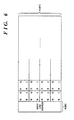
- Fig. 4 is a block diagram of the FLCD 109 of this embodiment.
- reference numeral 400 denotes a controller for controlling the entire FLCD; and 401, an FLC panel.
- Reference numeral 402 denotes a circuit for selecting one of the lines in the row direction of the FLC panel 401; and 403, a register having a one-line memory capacity.
- the controller 400 receives the data having the format shown in Fig. 6 from the display controller 108, checks its start write address, and supplies data of the subsequently received pixel data RGBIRGBI... to the register 403.
- the controller 400 outputs an instruction to cause the row selection circuit 402 to select the line designated by the write address, thereby updating the display of the FLC panel 401.
- the controller 400 outputs a data transfer request signal to the display controller 108 every time interval (varying within the range of 60 to 70 ⁇ sec.) depending on the temperature obtained from a temperature sensor (not shown).
- the frame memory control circuit 307 when a 32-line transfer request is designated from the CPU 300, the frame memory control circuit 307 outputs data in units of lines in accordance with the above-mentioned format upon reception of every data transfer request. When transfer of all the designated lines is completed, and the next transfer request instruction is not received, if a data transfer request signal is received from the FLCD 109, the frame memory control circuit 307 notifies the CPU 300 of this fact in the form of an interrupt signal.
- the CPU 300 determines whether nontransferred data of a partially rewritten image is present. If such nontransferred data is absent, the image data of all the frame stored in the frame memory 306 is designated and transferred to the FLCD 109 by the interlace scan. More specifically, every time this interrupt signal is received, the CPU 300 outputs an instruction to the frame memory control circuit 307 such that data is transferred in units of lines in the order of the 1st line, the third line,..., the 1023rd line, the second line,..., 1024th line. Note that when a transfer request signal is input from the FLCD 109, the CPU 300 designates a line to be transferred upon reception of the next transfer request signal.
- the interlace scan is used to transfer data due to the following reason.
- the FLCD 109 used in this embodiment has a function of storing and retaining the display image, as previously described. Therefore, only the image of an updated portion need be theoretically transferred. However, a small difference may occur in luminance at the boundary between an image which has not changed and need not be refreshed and an image which has changed and newly driven and displayed (partially rewritten image), thereby using the interlace scheme.
- the FLCD 109 of this embodiment updates the display only at the updated portion. However, when no change is made in the display image, all the image in the frame memory 306 is transferred to the FLCD 109 by the interlace scan. Transfer is not performed in units of lines, but transfer is performed by the interlace scan due to the following reason. Since a liquid crystal display does not have a high response speed, the apparent updating speed of the display image is increased.
- Image data finally transferred to the FLCD 109 in the display controller 108 of this embodiment is stored not in the VRAM 301, but in the frame memory 306.
- Fig. 5 shows only the portion associated with this check, and the remaining portion is not illustrated. However, the check portion can be sufficiently understood from the contents of the above description.
- reference numeral 501 denotes a line address generation circuit for generating start address information (i.e., information representing the line number of desired data of the FLCD 109; start word information in Fig. 6) of data to be transferred to the FLCD 109.
- start address information i.e., information representing the line number of desired data of the FLCD 109; start word information in Fig. 6
- the line address designated by the CPU 300 is set for the line address generation circuit 501, and that the line address generation circuit 501 updates the address to the next line for every 1-line transfer if a plurality of transfer lines are present.
- Reference numeral 502 denotes a FIFO memory capable of storing image data (RGBI) of 1 address information + 1-line image data.
- RGBI image data
- one line has 1,280 pixels
- Reference numeral 504 denotes a latch circuit; and 505, a register for storing an address designated by the CPU 300.
- Reference numeral 506 denotes a counter.
- image data of 1 address + 1-line image data is transferred from the FIFO memory 502 to the FLCD 109 (i.e., the active period of a transfer enable signal (not shown))
- the counter 506 counts transfer clocks (not shown) during this period.
- the counter 506 outputs a latch signal twice, i.e., two consecutive clocks to the latch 504.
- the CPU 300 stores an arbitrary address of transfer data in the register 505 and causes the frame memory control circuit 307 to perform transfer of a desired line.
- the latch 504 can hold the data of this arbitrary address (an arbitrary address location in one line) of the line and the next data. More specifically, two arbitrary words (8-pixel data) in the designated transfer data can be extracted.
- the CPU 300 When the CPU 300 reads out the data currently stored in the latch 504, the CPU 300 can check data to be transferred to the FLCD 109. Of course, "0" can be set in the register 505 to extract the contents of the write line address.
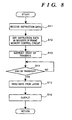
- step S1 the CPU 101 reads out sample image data or data for drawing this sample image from the HDD or the like and transfers it to the display controller 108 (accurately the VRAM 301) or causes the display controller 108 to draw the sample image.
- the display controller 108 accurately the VRAM 301
- a graphic cursor interlocked with a pointing device is not generally displayed due to the following reason. When the cursor is displayed during the check period and moves, write access to the VRAM 301 is performed by this movement, and the conversion result may exceed a predicted result.
- step S2 The flow advances to step S2 to check if the check is completed. If YES in step S2, the flow advances to step S3 to instruct the CPU 300 in the display controller 108 to read a specific word address of a line having a specific line number.
- processing returns to step S2 so as to output the next instruction.
- step S5 the flow advances to step S5 to perform processing for storing the noncoincident data and its position in the main memory 104 (or the HDD or the like). The flow then returns to step S2.
- step S6 If the check of the one-frame data is completed, the flow advances to step S6. If no abnormal data is present in the main memory 104, a message representing a normal check result is displayed. If abnormal data is present in the main memory 104, a message representing the specific position of the abnormal data is displayed. Note that notification need not be limited to the display of messages, but may be performed by an ON operation or flickering of a predetermined LED or tone generation by a buzzer or the like.
- step S11 the CPU 300 fetches the designated data from the CPU 101.
- step S12 the CPU 300 sets a word address extracted from a line address indicated by the designated data in the register 505 in the frame memory control circuit 307. The line address designated in the same manner as described is set, and the CPU 300 transfers the image data of this line to the FLCD 109 (step S13).
- the frame memory control circuit 307 Upon completion of this transfer, the frame memory control circuit 307 outputs an interrupt signal to the CPU 300, and the CPU 300 detects this interrupt signal (step S14).
- step S15 to cause the frame memory control circuit 307 to read out the data held in the latch.
- the readout data is output to the CPU on the information processing system side in step S16.
- the test can be diagnosed whether processing in the display controller 108 is normally performed.
- the test need not be performed while observing the screen on the FLCD 109, so that the check operation can be greatly facilitated.
- the check processing has been described while mainly assuming the manufacturing process.
- the check processing may also be performed in an environment where the user actually uses the apparatus. In this case, the check processing may be performed in the initialization stage upon power-ON of the information processing apparatus. Alternatively, the check processing may be executed when the user designates it as needed.
- the FIFO memory 307a is actually connected to the FLCD 109 through an interface cable, and a display controller interface, an FLCD interface, a line driver, and a line receiver are arranged for the display controller 108 and the FLCD 109. Therefore, solder and patterns on the boards of the display controller 108 and the FLCD 109, radiation noise reduction filters, and connectors fall outside the range of check processing.
- Fig. 9 is a block diagram of an FLCD 109 of the second embodiment.
- the FLCD 109 of the second embodiment is different from that of Fig. 4 in that a FIFO serving as a buffer for synchronizing a serial interface 404 with the system is arranged.
- the remaining arrangement in Fig. 9 is same as that of Fig. 4.
- the serial interface 404 is a versatile interface such as an RS232C interface.
- the reason why the versatile interface is used is that an interface such as an RS232C interface is generally a standard interface in an apparatus (e.g., a personal computer or a workstation) to which the FLCD is connected.
- Fig. 10 shows the connection relationship between an information processing system (apparatus), the FLCD 109, and a display controller according to the second embodiment.
- a serial cable from the FLCD 109 is connected to the serial interface (RS232C) on the information processing system side.
- RS232C serial interface
- a CPU 101 on the information processing system side outputs a command for testing the FLCD 109 through a serial port arranged in the apparatus itself and writes a sample image in a VRAM 301 in a display controller 108.
- the display controller 108 outputs line data to the FLCD 109 or designates a line address to be transferred to a CPU 300 in the display controller 108, as a normal operation.
- a controller 400 on the FLCD 109 side outputs the data from the display controller 108 in the reception order to the information processing system through the serial interface 404.
- the CPU 101 on the information processing system side outputs a transfer instruction, receives the data (write line address + 1-line data) received through the serial port, and checks matching. Note that the transfer order may be determined by the interlace scan. In this case, since the line data is sent with a line address, the display data can be reconstructed on the information processing system side in accordance with the line address.
- a check image may be or may not be displayed on the FLCD 109 during the check period.
- the information volume to be checked is given in units of 2 words, i.e., 8 pixels.
- the transferred data is sent back at once due to the following reason.
- Serial communication has a transfer rate lower than that of the first embodiment. If transfer is performed in units of bytes, the overhead amount excessively increases. If check processing is performed through an interface which does not limit the transfer rate, the above limitation is not imposed. For example, when the display controller 108 and the FLCD 109 are connected through a bidirectional communication interface, an additional interface need not be arranged for the FLCD.
- a frame memory control circuit 307 in the above embodiment does not output an interrupt signal responsive to a data transfer request signal from the FLCD 109 to the CPU 300 during the transfer of the partially rewritten image.
- the frame memory control circuit 307 may output an interrupt signal regardless of its operating state.
- the CPU 300 when the CPU 300 outputs a partial rewrite instruction, the CPU 300 has detected the number of lines to be transferred. Every time an interrupt is received, the CPU 300 decrements the number of lines and checks the count value. Therefore, the CPU 300 can detect whether an interrupt is caused by the end of transfer or an interrupt is generated during transfer by interlace scan.
- the processing sequences of the CPUs 101 and 300 in the above embodiments are merely examples, and the present invention is not limited to these sequences. It is essential to interpose a frame memory 306 in transfer of a partially rewritten image to the FLCD in an asynchronous manner.
- the display controller 108 or the FLCD 109 may be arranged integrally with an information processing apparatus as a standard equipment, or may be mounted in a standard expansion slot of an apparatus represented by a personal computer.
- the CPU 300 in the display controller 108 performs processing in accordance with the program stored in a ROM 308.
- a RAM or a programmable, memory retainable EEPROM may be used in place of the ROM 308.
- the corresponding program is downloaded to the CPU 300 in the display controller 108 in the initial stage of driver software for driving the FLCD interface upon power-ON on the information processing apparatus side.
- the use of the RAM or EEPROM can facilitate a change in processing program of the CPU 300 and debugging of the program.
- the information processing apparatus or an FLCD interface apparatus may be a single apparatus or a combination of a plurality of apparatuses, or may be applied when an external program is supplied.
- Each embodiment described above has exemplified an FLCD, i.e., a ferroelectric liquid crystal display.
- the number of display colors is 16.
- the present invention is not limited to these, either.
- the present invention is applicable to any apparatus in which image data stored in a VRAM is subjected to some processing, and the processed data is displayed.
- converted image data corresponding to a display can be obtained and need not be visually checked.
- Each embodiment described above has exemplified an FLCD, i.e., a ferroelectric liquid crystal display.
- the number of display colors is 16.
- the present invention is not limited to these, either.
- the present invention is applicable to any apparatus in which image data stored in a VRAM is subjected to some processing, and the processed data is displayed.
- the conversion circuit extracts data at a position designated from a host apparatus from image data output to the display device, and outputs the extracted data to the host apparatus.
- image data obtained upon normal conversion in the conversion circuit is prepared in advance, and this image data is collated with the data sent from the conversion circuit to determine whether the operation of the conversion circuit is normal.
Landscapes
- Engineering & Computer Science (AREA)
- Physics & Mathematics (AREA)
- Computer Hardware Design (AREA)
- General Physics & Mathematics (AREA)
- Theoretical Computer Science (AREA)
- Chemical & Material Sciences (AREA)
- Crystallography & Structural Chemistry (AREA)
- Liquid Crystal Display Device Control (AREA)
- Control Of Indicators Other Than Cathode Ray Tubes (AREA)
- Testing, Inspecting, Measuring Of Stereoscopic Televisions And Televisions (AREA)
Claims (9)
- Gerät zum Ausführen einer Steuerung einer Anzeige, gekennzeichnet durch:gekennzeichnet durch:ein erstes Speichermittel (301), das Originalbilddaten eines anzuzeigenden Bildes speichert;ein zweites Speichermittel (306), das Daten in einem Format speichert, das geeignet ist zur Anzeige auf der Anzeige; undein Umsetzmittel (305), das die Bilddaten umsetzt, die im ersten Mittel gespeichert sind, in ein Datenformat, das zur Anzeige auf der Anzeige und zur Ausgabe der umgesetzten Daten an das zweite Speichermittel geeignet ist;wobei der Befehl aus dem Hauptgerät eine Zeilenadresse des zur Anzeige übertragenen Bildes und eine Positionsadresse auf der Grundlage einer Einheit des Übertragens enthält.ein Ausgabemittel (307) zum Ausgeben wenigstens eines Teils der aus dem zweiten Speichermittel zur Anzeige (109) zu einem Hauptgerät gemäß einem vorbestimmten Befehl aus dem Hauptgerät übertragenen Daten;
- Gerät nach Anspruch 1, bei dem die Anzeige Speichereigenschaften des Anzeigeinhalts besitzt.
- Gerät nach Anspruch 2, bei dem die Anzeige eine ferroelektrische Flüssigkristallanzeige ist.
- Gerät nach Anspruch 1, das des weiteren eingerichtet ist, an einen im Hauptgerät eingerichteten Erweiterungsbus angeschlossen zu werden, wobei dieses ein Informationsverarbeitungsgerät ist.
- Informationsverarbeitungsgerät mit einem Anzeigesteuergerät nach Anspruch 1.
- Gerät nach Anspruch 1, das des weiteren eingerichtet ist, über ein Kabel mit einem Informationsverarbeitungsgerät verbunden zu werden in Hinsicht darauf, welches Gerät zur Ausführung der Steuerung der Anzeige eine unabhängige externe Einrichtung ist.
- Gerät nach Anspruch 1, dessen Hauptgerät eingerichtet ist zum Überprüfen der Datenabgabe durch das Ausgabemittel an das Hauptgerät.
- Verfahren zum Ausführen einer Steuerung einer Anzeige, gekennzeichnet durch die Verfahrensschritte:gekennzeichnet durch den weiteren Verfahrensschritt:Speichern von Originalbilddaten eines anzuzeigenden Bildes in einem ersten Speichermittel (301); undUmsetzen der im ersten Speichermittel gespeicherten Daten in ein Datenformat, das geeignet ist zur Anzeige auf einer Anzeige und Speichern der umgesetzten Daten im zweiten Speichermittel (306) ;wobei der Befehl aus dem Hauptgerät eine Zeilenadresse des zur Anzeige übertragenen Bildes und eine Positionsadresse auf der Grundlage einer Einheit des Übertragens enthält.Ausgeben wenigstens eines Teiles der aus dem zweiten Speichermittel zur Anzeige (109) an ein Hauptgerät übertragenen Daten gemäß einem vorbestimmten Befehl aus dem Hauptgerät;
- Verfahren nach Anspruch 8, mit dem weiteren Verfahrensschritt:Überprüfen der Daten der an das Hauptgerät abgegebenen Daten im Verfahrensschritt des Ausgebens durch das Hauptgerät.
Applications Claiming Priority (6)
| Application Number | Priority Date | Filing Date | Title |
|---|---|---|---|
| JP32259/95 | 1995-02-21 | ||
| JP03225995A JP3281502B2 (ja) | 1995-02-21 | 1995-02-21 | 表示制御装置及び情報処理装置及び制御方法 |
| JP3225995 | 1995-02-21 | ||
| JP4832095 | 1995-03-08 | ||
| JP48320/95 | 1995-03-08 | ||
| JP7048320A JPH08248391A (ja) | 1995-03-08 | 1995-03-08 | 表示制御装置及び情報処理装置及び制御方法 |
Publications (3)
| Publication Number | Publication Date |
|---|---|
| EP0729129A2 EP0729129A2 (de) | 1996-08-28 |
| EP0729129A3 EP0729129A3 (de) | 1999-09-15 |
| EP0729129B1 true EP0729129B1 (de) | 2002-10-23 |
Family
ID=26370801
Family Applications (1)
| Application Number | Title | Priority Date | Filing Date |
|---|---|---|---|
| EP96102531A Expired - Lifetime EP0729129B1 (de) | 1995-02-21 | 1996-02-20 | Anzeigesystem und -verfahren mit einer Bildumwandlung, die ohne visuelle Inspektion kontrolliert werden kann |
Country Status (4)
| Country | Link |
|---|---|
| US (1) | US5907329A (de) |
| EP (1) | EP0729129B1 (de) |
| KR (1) | KR100220131B1 (de) |
| DE (1) | DE69624394T2 (de) |
Families Citing this family (9)
| Publication number | Priority date | Publication date | Assignee | Title |
|---|---|---|---|---|
| JPH11338427A (ja) * | 1998-05-22 | 1999-12-10 | Fujitsu Ltd | 表示装置 |
| US6246386B1 (en) * | 1998-06-18 | 2001-06-12 | Agilent Technologies, Inc. | Integrated micro-display system |
| EP0967588A1 (de) * | 1998-06-23 | 1999-12-29 | Koninklijke Philips Electronics N.V. | Anzeigesteuergerät mit Animationsschaltung |
| US6308298B1 (en) | 1998-11-16 | 2001-10-23 | Ecrix Corporation | Method of reacquiring clock synchronization on a non-tracking helical scan tape device |
| JP3105884B2 (ja) | 1999-03-31 | 2000-11-06 | 新潟日本電気株式会社 | メモリ性表示装置用表示コントローラ |
| KR100617206B1 (ko) * | 1999-07-06 | 2006-08-31 | 엘지전자 주식회사 | 디지털 티브이의 av 데이터 저장포맷 변경 장치 및 방법 |
| JP4031618B2 (ja) * | 2001-02-28 | 2008-01-09 | 安西メディカル株式会社 | 放射線源検出装置 |
| US6965387B2 (en) * | 2001-08-03 | 2005-11-15 | Ball Semiconductor, Inc. | Real time data conversion for a digital display |
| JP4046716B2 (ja) * | 2004-10-06 | 2008-02-13 | 株式会社ソニー・コンピュータエンタテインメント | 情報処理装置およびデータ伝送方法 |
Family Cites Families (7)
| Publication number | Priority date | Publication date | Assignee | Title |
|---|---|---|---|---|
| JP2579933B2 (ja) * | 1987-03-31 | 1997-02-12 | キヤノン株式会社 | 表示制御装置 |
| US5020116A (en) * | 1989-12-13 | 1991-05-28 | Hughes Aircraft Company | Image registration method and apparatus |
| US5055928A (en) * | 1990-04-10 | 1991-10-08 | Sony Corporation Of America | Digital video frame recorder with video display test pattern signal generator |
| DE69321873T2 (de) * | 1992-05-19 | 1999-05-20 | Canon Kk | Verfahren und Einrichtung zur Steuerung einer Anzeige |
| EP0579359B1 (de) * | 1992-05-19 | 1997-09-24 | Canon Kabushiki Kaisha | Verfahren und Einrichtung zur Steuerung einer Anzeige |
| JPH05323905A (ja) * | 1992-05-19 | 1993-12-07 | Canon Inc | 表示制御装置 |
| JPH05323904A (ja) * | 1992-05-19 | 1993-12-07 | Canon Inc | 表示制御装置及び表示制御方法 |
-
1996
- 1996-02-20 EP EP96102531A patent/EP0729129B1/de not_active Expired - Lifetime
- 1996-02-20 DE DE69624394T patent/DE69624394T2/de not_active Expired - Lifetime
- 1996-02-20 US US08/603,712 patent/US5907329A/en not_active Expired - Fee Related
- 1996-02-21 KR KR1019960004041A patent/KR100220131B1/ko not_active IP Right Cessation
Also Published As
| Publication number | Publication date |
|---|---|
| EP0729129A2 (de) | 1996-08-28 |
| DE69624394T2 (de) | 2003-06-12 |
| EP0729129A3 (de) | 1999-09-15 |
| KR960032287A (ko) | 1996-09-17 |
| DE69624394D1 (de) | 2002-11-28 |
| KR100220131B1 (ko) | 1999-09-01 |
| US5907329A (en) | 1999-05-25 |
Similar Documents
| Publication | Publication Date | Title |
|---|---|---|
| US7242370B2 (en) | Display apparatus, method of controlling the same, and multidisplay system | |
| JP3066597B2 (ja) | ラスターデータの変化を検出するための方法および装置 | |
| EP0570906B1 (de) | Verfahren und Einrichtung zur Steuerung einer Anzeige | |
| EP0591682B1 (de) | Verfahren und Einrichtung zur Steuerung einer Anzeige | |
| EP0708433B1 (de) | Verfahren und Einrichtung zum Steuern einer Anzeige | |
| EP0918278B1 (de) | Schaltung zum simultanen Ansteuern eines Flüssigkristall-Bildschirms und eines Fernsehbildschirms | |
| EP0729129B1 (de) | Anzeigesystem und -verfahren mit einer Bildumwandlung, die ohne visuelle Inspektion kontrolliert werden kann | |
| EP0535622A2 (de) | Steuersystem für eine flache Anzeigetafel | |
| US5374941A (en) | Display control apparatus for dispersionless display | |
| KR100375531B1 (ko) | 복수의 연쇄 디스플레이 장치의 구동 방법, 구동 장치,연쇄 가능한 디스플레이 장치, 및 연쇄 디스플레이 시스템 | |
| EP0663660B1 (de) | System zur Verbesserung der Formatveränderungen in ferroelektrischen Flüssigkristallanzeigen | |
| US20010043206A1 (en) | Display control device | |
| EP0591683A1 (de) | Verfahren und Einrichtung zur Steuerung einer Anzeige | |
| US5905483A (en) | Display control apparatus | |
| EP0348479A1 (de) | Verfahren zum unterteilen einer figur in bereiche in einem graphischen anzeigesystem | |
| JP2002032063A (ja) | 液晶表示装置およびウィンドウ表示拡大制御方法 | |
| EP0592801A1 (de) | Verfahren und Einrichtung zur Steuerung einer Anzeige | |
| US5856817A (en) | Display control method and display controller and display apparatus using the same | |
| JP3281502B2 (ja) | 表示制御装置及び情報処理装置及び制御方法 | |
| JPH09274475A (ja) | 1台のコンピュータに複数台接続可能な表示装置 | |
| JP3227200B2 (ja) | 表示制御装置及び方法 | |
| JPH08248391A (ja) | 表示制御装置及び情報処理装置及び制御方法 | |
| JPH08334739A (ja) | 表示装置及びその表示制御装置及び情報処理装置 | |
| JP2001100686A (ja) | 表示データ取込方法及び比較検査装置 | |
| US20050001809A1 (en) | Robust LCD controller |
Legal Events
| Date | Code | Title | Description |
|---|---|---|---|
| PUAI | Public reference made under article 153(3) epc to a published international application that has entered the european phase |
Free format text: ORIGINAL CODE: 0009012 |
|
| AK | Designated contracting states |
Kind code of ref document: A2 Designated state(s): DE FR GB IT NL |
|
| PUAL | Search report despatched |
Free format text: ORIGINAL CODE: 0009013 |
|
| AK | Designated contracting states |
Kind code of ref document: A3 Designated state(s): DE FR GB IT NL |
|
| 17P | Request for examination filed |
Effective date: 20000128 |
|
| 17Q | First examination report despatched |
Effective date: 20000628 |
|
| GRAG | Despatch of communication of intention to grant |
Free format text: ORIGINAL CODE: EPIDOS AGRA |
|
| GRAG | Despatch of communication of intention to grant |
Free format text: ORIGINAL CODE: EPIDOS AGRA |
|
| GRAH | Despatch of communication of intention to grant a patent |
Free format text: ORIGINAL CODE: EPIDOS IGRA |
|
| GRAH | Despatch of communication of intention to grant a patent |
Free format text: ORIGINAL CODE: EPIDOS IGRA |
|
| GRAA | (expected) grant |
Free format text: ORIGINAL CODE: 0009210 |
|
| AK | Designated contracting states |
Kind code of ref document: B1 Designated state(s): DE FR GB IT NL |
|
| PG25 | Lapsed in a contracting state [announced via postgrant information from national office to epo] |
Ref country code: NL Free format text: LAPSE BECAUSE OF FAILURE TO SUBMIT A TRANSLATION OF THE DESCRIPTION OR TO PAY THE FEE WITHIN THE PRESCRIBED TIME-LIMIT Effective date: 20021023 Ref country code: IT Free format text: LAPSE BECAUSE OF FAILURE TO SUBMIT A TRANSLATION OF THE DESCRIPTION OR TO PAY THE FEE WITHIN THE PRESCRIBED TIME-LIMIT;WARNING: LAPSES OF ITALIAN PATENTS WITH EFFECTIVE DATE BEFORE 2007 MAY HAVE OCCURRED AT ANY TIME BEFORE 2007. THE CORRECT EFFECTIVE DATE MAY BE DIFFERENT FROM THE ONE RECORDED. Effective date: 20021023 |
|
| REG | Reference to a national code |
Ref country code: GB Ref legal event code: FG4D |
|
| REF | Corresponds to: |
Ref document number: 69624394 Country of ref document: DE Date of ref document: 20021128 |
|
| ET | Fr: translation filed | ||
| NLV1 | Nl: lapsed or annulled due to failure to fulfill the requirements of art. 29p and 29m of the patents act | ||
| PLBE | No opposition filed within time limit |
Free format text: ORIGINAL CODE: 0009261 |
|
| STAA | Information on the status of an ep patent application or granted ep patent |
Free format text: STATUS: NO OPPOSITION FILED WITHIN TIME LIMIT |
|
| 26N | No opposition filed |
Effective date: 20030724 |
|
| PGFP | Annual fee paid to national office [announced via postgrant information from national office to epo] |
Ref country code: FR Payment date: 20120312 Year of fee payment: 17 |
|
| PGFP | Annual fee paid to national office [announced via postgrant information from national office to epo] |
Ref country code: DE Payment date: 20120229 Year of fee payment: 17 |
|
| PGFP | Annual fee paid to national office [announced via postgrant information from national office to epo] |
Ref country code: GB Payment date: 20120224 Year of fee payment: 17 |
|
| GBPC | Gb: european patent ceased through non-payment of renewal fee |
Effective date: 20130220 |
|
| REG | Reference to a national code |
Ref country code: FR Ref legal event code: ST Effective date: 20131031 |
|
| REG | Reference to a national code |
Ref country code: DE Ref legal event code: R119 Ref document number: 69624394 Country of ref document: DE Effective date: 20130903 |
|
| PG25 | Lapsed in a contracting state [announced via postgrant information from national office to epo] |
Ref country code: DE Free format text: LAPSE BECAUSE OF NON-PAYMENT OF DUE FEES Effective date: 20130903 Ref country code: FR Free format text: LAPSE BECAUSE OF NON-PAYMENT OF DUE FEES Effective date: 20130228 Ref country code: GB Free format text: LAPSE BECAUSE OF NON-PAYMENT OF DUE FEES Effective date: 20130220 |