EP0726687B1 - Funktelefon - Google Patents
Funktelefon Download PDFInfo
- Publication number
- EP0726687B1 EP0726687B1 EP96300472A EP96300472A EP0726687B1 EP 0726687 B1 EP0726687 B1 EP 0726687B1 EP 96300472 A EP96300472 A EP 96300472A EP 96300472 A EP96300472 A EP 96300472A EP 0726687 B1 EP0726687 B1 EP 0726687B1
- Authority
- EP
- European Patent Office
- Prior art keywords
- system clock
- mobile telephone
- clock
- telephone according
- sleep
- Prior art date
- Legal status (The legal status is an assumption and is not a legal conclusion. Google has not performed a legal analysis and makes no representation as to the accuracy of the status listed.)
- Expired - Lifetime
Links
Images


Classifications
-
- H—ELECTRICITY
- H04—ELECTRIC COMMUNICATION TECHNIQUE
- H04W—WIRELESS COMMUNICATION NETWORKS
- H04W52/00—Power management, e.g. TPC [Transmission Power Control], power saving or power classes
- H04W52/02—Power saving arrangements
- H04W52/0209—Power saving arrangements in terminal devices
- H04W52/0261—Power saving arrangements in terminal devices managing power supply demand, e.g. depending on battery level
- H04W52/0287—Power saving arrangements in terminal devices managing power supply demand, e.g. depending on battery level changing the clock frequency of a controller in the equipment
- H04W52/029—Power saving arrangements in terminal devices managing power supply demand, e.g. depending on battery level changing the clock frequency of a controller in the equipment reducing the clock frequency of the controller
-
- Y—GENERAL TAGGING OF NEW TECHNOLOGICAL DEVELOPMENTS; GENERAL TAGGING OF CROSS-SECTIONAL TECHNOLOGIES SPANNING OVER SEVERAL SECTIONS OF THE IPC; TECHNICAL SUBJECTS COVERED BY FORMER USPC CROSS-REFERENCE ART COLLECTIONS [XRACs] AND DIGESTS
- Y02—TECHNOLOGIES OR APPLICATIONS FOR MITIGATION OR ADAPTATION AGAINST CLIMATE CHANGE
- Y02D—CLIMATE CHANGE MITIGATION TECHNOLOGIES IN INFORMATION AND COMMUNICATION TECHNOLOGIES [ICT], I.E. INFORMATION AND COMMUNICATION TECHNOLOGIES AIMING AT THE REDUCTION OF THEIR OWN ENERGY USE
- Y02D30/00—Reducing energy consumption in communication networks
- Y02D30/70—Reducing energy consumption in communication networks in wireless communication networks
Definitions
- the present invention relates to a radio telephone having a high frequency system clock and processing means.
- the present invention relates to a radio telephone in which said processing means is arranged to process polling signals received during a predetermined portion of a repeated periodic cycle.
- a highly accurate high frequency system clock produces a clock signal at a frequency in the tens of megahertz.
- the clocking signal is required continuously, so as to accurately align transmitted data and received data within a time and frequency multiplex established by an operating network.
- a problem with mobile telephones of this type is that the processing circuitry demands significant levels of battery power, therefore it is desirable to de-activate this circuitry when it is not actually required.
- de-activation periods may be assessed with reference to a predetermined count of system clock pulses.
- this in itself represents a component which places significant demands upon the power supply and, preferably, it would be desirable to de-activate the system clock when it is not actually required.
- this creates a problem, given that, under normal circumstances, it would be the system clock itself which provided a measure of de-activation periods.
- European Patent Publication No. 0 586 256 discloses a mobile telephone in which a relatively low quality, low frequency clock is provided in addition to the high frequency system clock.
- a system clock is used to determine the accuracy and stability of the low frequency clock, hence allowing said clock to be calibrated with reference to the system clock. It is then possible to de-activate the system clock for predetermined durations, during which said clock may be referred to as entering a "sleep mode". The duration is measured with reference to the low frequency "sleep clock", whereafter the high frequency system clock is re-activated for the subsequent processing of data.
- the system clock is required to be re-activated in anticipation of receiving polling signals, contained within a specific polling frame within each superframe. Thereafter, a sleep duration may be assessed and measured by counting pulses generated by the sleep clock. Thereafter, the system clock is re-activated in anticipation of receiving the next burst of polling signals.
- a problem with this known proposal is that further processing time must be used in order to calibrate the sleep clock. Furthermore, conditions may exist during which the sleep clock frequency varies to such an extent that it is not possible to enter sleep mode for a significant number of cycles. Thus, in order to maintain effective and active calibration of the sleep clock, it is necessary to perform substantially more additional processing so as to effect the calibration which in turn offsets savings made in terms of being able to enter sleep mode.
- a mobile telephone having a high frequency system clock and processing means arranged to process polling signals received during a predetermined portion of a repeated periodic cycle, comprising first counting means for counting system clock pulses; a low frequency sleep clock; second counting means for counting sleep clock pulses; means for de-activating the system clock; means for re-activating said system clock after a calibrated number of sleep clock pulses; means for re-loading the first counting means; and calibration means for calibrating the calibrated number by comparing the re-set system clock count with base station timing signals.
- the invention provides the advantage of giving accurate sleep clock calibration while minimising additional requirements on processing time and hardware.
- the first counting means is re-set to specify a new sub-frame and frame count consistent with the re-activation time.
- the system clock is de-activated after the completion of cycle processing.
- de-activation occurs at the optimum time, so as to maximise sleep durations.
- system clock re-activation occurs at a predetermined position within each repeated periodic cycle.
- re-activation points are generated independently of de-activation points and it is not necessary for the system to calculate sleep durations.
- Comparisons with base station timing signals may be made at any appropriate rate.
- the re-loaded system clock count is compared with base station timing signals on each cycle.
- a calibrated number is also calibrated on each cycle so as to optimise system re-activation on each cycle.
- a mobile telephone is shown in Figure 1, contained within a plastic housing 15, with an antenna 16 extending from said housing to facilitate communication between the mobile telephone and cellular base stations.
- the telephone includes an earpiece 18 and a microphone 19, along with manually operable keys 20 and a liquid crystal display 21.
- the telephone includes an on/off switch 22 such that, when not required, the telephone may be switched off so as to conserve battery power.
- a nickelcadmium battery pack is attachable to the rear of the telephone and the ability to conserve battery power will significantly affect the duration between battery recharging or battery replacement.
- the telephone When switched on, by operation of switch 22, the telephone has essentially two modes of operation. In a first mode, the telephone is placed in a stand-by condition. In this stand-by condition, the telephone is not usable as such but remains active, so that it is receptive to polling signals transmitted by base stations. Furthermore, it is also in a condition responsive to manual key operation. Thus, in its stand-by condition, the telephone is effectively waiting for a call to be established by the telephone user or by someone wishing to contact the telephone user.
- the telephone When a call is set up either by the telephone user or by someone calling the user, the telephone must enter its second mode of operation, under which communication channels are established between the telephone and a cellular base station.
- the telephone communicates with base stations using an encoded digital time-multiplex, in which an allocated transmission frequency band is divided, over time, into a plurality of channel frames.
- An operational network will have a plurality of radio frequencies allocated thereto and the total number of frequencies will determine the total number of calls which may be simultaneously connected within each particular cell.
- signalling commands so as to facilitate the connection of calls and the switching of communications between base stations.
- the signalling instructions are also transmitted using the frame structure, therefore some frames will have a different character to that of others. It is necessary for the system, at any particular time, to be aware of the type of frame that is being transmitted, therefore the frame structure is repeated in a predictable way.
- each transmitted frame contains a fixed number of data symbols and a predetermined number of these frames constitute the total period of a repeated cycle.
- a group of repeated frames is referred to as a superframe, or multiframe, and a superframe structure for the present embodiment is shown in Figure 2.
- the superframe is transmitted over 720 milliseconds and includes a total of thirty six frames 22.
- Frame 23, shown shaded in Figure 2 includes polling information which may be considered as a burst of information identifying unique numbers for particular mobile telephones, thereby identifying telephones which are being called and require a call to be answered.
- polling information may be considered as a burst of information identifying unique numbers for particular mobile telephones, thereby identifying telephones which are being called and require a call to be answered.
- a frame 22 is detailed in Figure 3 and consists of 6720 sub-frame periods.
- the sub-frame period frequency defines the output sample rate, therefore it is necessary for the output digital circuitry to produce an output value at the sub-frame period rate and, similarly, input signals are sampled at this rate.
- each frame includes a transmit portion 31 and a receive portion 32, separated by an idle portion 33.
- data is transmitted from the mobile telephone to a base station at the sub-frame rate while, similarly, during the receive portion, data is received by the mobile telephone at this rate.
- the whole system operates within an accurately synchronised environment in which the clocking of signals within each mobile telephone must be synchronised to clocking signals generated by base stations.
- the mobile telephone includes an accurate system clock arranged to produce clocking signals at 16.8 MHz.
- Internal circuitry within the mobile telephone including a digital signal processing circuit, receives these processor clock signals directly and executes instructions in response to these signals.
- Timing signals, to identify the start of sub-frames, frames and super frames are generated by counting system- clock signals in a cascaded chain of counters or frequency dividers. Such a chain is illustrated in Figure 4.
- An output from a system clock 41 at 16.8 MHz is supplied to a first frequency divider 42 arranged to divide the system clock's frequency by 50.
- the first counter 42 produces sub-frame clocks at 336 kHz, each identifying the start of a sub-frame period, as identified in Figure 3.
- the output from counter 42 is also supplied to a second counter 43, arranged to divide the clock frequency by 6720. Referring to Figure 3, it can be seen that each frame is made up of 6720 sub-frame periods, therefore the output from counter 43 produces clocking signals at the frame rate of 50 Hz.
- the output from counter 43 is supplied to a third counter 44, arranged to divide the clocking frequency by 36, to produce superframe clocks at 1.38 Hz.
- the output from counters 42, 43 and 44 identifies a particular sub-frame period, within a particular frame of a superframe. These values are also compared with reference signals received from base stations and, where appropriate, modifications are made to the counters so as to bring the operation of the mobile telephone accurately into phase with network clocks. Thus, during each superframe cycle, the mobile telephone may compare its internal clocking signals with network clocks, to ensure that the operation of the mobile telephone is accurately synchronised to the network.
- each polling burst 51 represents a period during which the telephone must be active and capable of receiving and analysing information transmitted during the polling burst.
- intervals 52 it is not necessary for the telephone to communicate with base stations, given that no polling information is being transmitted.
- the telephone may be required to perform other processing operations, therefore it will be necessary for the telephone to remain active for a short period after the transmission of the polling burst.
- the operation of the telephone must have stabilised prior to the polling burst being transmitted, therefore it is necessary for the system clock to be activated slightly before the polling burst is transmitted.
- Each active period 53 starts at a predetermined interval before a polling burst 51 is transmitted.
- the telephone remains active throughout the transmission of the polling burst 51 and may then de-activate after processing has been completed.
- sleep duration 54 a duration is provided, identified as sleep duration 54, during which the system clock may be de-activated, effectively placing the telephone into a sleep condition.
- the duration of the active intervals is variable, given that the degree of processing required by the telephone will also vary from cycle to cycle.
- a lower frequency sleep clock is included, which may be calibrated with reference to the system clock.
- a routine is included that calculates the duration of the subsequent sleep period 54 during each active period 53.
- a system clock may then be de-activated and the system placed in its sleep condition for the appropriate duration 54, as measured by the low frequency sleep clock.
- the sleep durations 54 are variable and the optimum point at which the system clock may be placed in its sleep mode will vary relative to the cycle phase.
- the duration of active pulses 53 is variable because the point at which de-activation occurs varies with reference to the cycle phase.
- an activation periodicity 55 is calculated.
- the sleep clock is calibrated with reference to the cycle clock, preferably on each cycle.
- the sleep clock is now arranged to calculate durations representing the periods between re-activation points.
- Circuitry is included which counts a predetermined number of sleep clock pulses during each cycle, so as to produce a re-activation pulse at the required point.
- the processor is arranged to effect a de-activating routine after completing the processing required for that particular cycle. In this way, de-activation occurs at the optimum point, after cycle processing, and it is not necessary to calculate a sleep duration. Re-activation then occurs at the predetermined position within the repeated cycle in anticipation of receiving polling signals. Thus, re-activation occurs prior to the polling burst being transmitted, allowing the circuitry to power up and stabilise.
- the system clock 41 and its associated counters 42, 43 and 44 are also shown in Figure 6. These devices communicate with a digital signal processor 61, which in turn receives external timing signals from base stations via an input line 62.
- the processor 61, the sleep clock 41 and associated counters may be placed into a sleep mode, during which the system clock 41 ceases to operate until re-activated by an interrupt signal supplied on a line 63 to the processor 61 from an adjustable counter 64.
- the adjustable counter in turn receives sleep clock pulses from a low frequency sleep clock 65, operating at approximately 32 kHz.
- a system clock clocks processor 61 via a clocking line 66.
- Counter 42 counts clock pulses from the system clock 41 to generate indications of the start of a sub-frame period, that are supplied to the processor 61 over a data line 67. These reduced frequency clocking pulses are also supplied to counter 43, which in turn supplies indications of the start of frame periods to the processor 61 over line 68.
- counter 44 receives an output from counter 43, as previously described, resulting in indications of the start of superframe periods being supplied to the processor 61 over a line 69.
- the processor 61 may keep a count of superframe periods but it should be appreciated that superframes represent the totality of a repeated cycle and each superframe contains a polling burst.
- the processor 61 is also arranged to supply new count values to said counters over lines 70, 71 and 72 respectively.
- the system phase may be restored by downloading new count values to the counters, whereafter they may be re-activated so as to continue counting signals generated by the system clock 41.
- the processor 61 also includes routines for checking that the counters 42, 43 and 44 are in phase with signals received from base stations, via line 62. Thus, the processor 61 may compare its local system phase with the network system phase and, where appropriate, modify count values, via data line 70, 71 or 72, so as to bring the count values into phase with the overall network. Thus, the processor 61 is capable of establishing the extent to which its own local system clock count may have drifted from the normal operating phase of the network.
- the sleep clock 65 generates sleep clock pulses that are in turn counted by the variable counter 64.
- the variable counter is controlled by the processor 61, which supplies a count value over line 73.
- the variable counter 64 is arranged to produce activation pulses at the activation periodicity 55, shown in Figure 5, by reducing the pulse frequency of the sleep clock.
- the counter 64 After counting a number of sleep pulses defined by the value supplied over line 73, the counter 64 generates a re-activation pulse over interrupt line 63, which in turn instructs the processor 61 to re-activate the system if said system has been placed in its sleep mode.
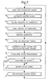
- Step 81 represents the processor 61 and system clock 41 in sleep mode, during which the system clock 41 is inactive.
- the processor 61 is effectively waiting for an activation pulse which, when received via line 63, activates the system clock 41.
- a short interval is provided, during which circuitry is allowed to power up and stabilise, such that normal processing may be resumed.
- the counters 42, 43 and 44 Prior to the resumption of normal processing, creating conditions such as to re-establish operation of the processor 61 and system clock 41 as if they had not been placed in sleep mode, the counters 42, 43 and 44 are re-loaded with new values, via data lines 70, 71 and 72 respectively. Thus, the processor 61 and system clock 41 are placed in sleep mode until the re-activation point. The period between re-activation points is specified in terms of a calibrated number of sleep clock pulses. Similarly, at the re-activation position, the system counters 42, 43 and 44 should have attained a specified number of system clock counts.
- step 86 the phase of the system counters 42, 43 and 44 is compared with external timing signals received over line 62. If necessary, modifications are made to the values stored in counters 42, 43 and 44 which, under normal operating conditions, would generally result in minor modifications being made to the sub-frame count of counter 43; it generally not being necessary to correct counter 42.
- the duration of a sleep clock pulse will not tend to represent an integer number of system clock pulses.
- the re-activation points will tend to drift, with reference to the optimum point defined in terms of system clock pulses, therefore re-calibration is required on a continual basis. Consequently, on each cycle, a re-calibration procedure is effected by making reference to the extent to which the system counters 42, 43 and 44 and in particular counter 43, are out of phase with the external timing signals received over line 62.
- the sleep clock may be perceived as having speeded up slightly, in which case fewer counts are required.
- the activation point will tend to drift, therefore occasionally a cycle is required in which fewer counts are made by counter 64 or more counts are made by counter 64. Thereafter, the count is re-adjusted on the next cycle and the process continues.
- the activation point, as determined by counter 64 may drift slightly with reference to the optimum point defined in terms of system clock pulses but, on each cycle, it will be modified such that the activation point, defined by the sleep clock, does not drift beyond an extent to which it is possible for the processor 61 to recover the situation, with reference to signals received externally.
- step 87 whereupon the sleep clock is calibrated and a new count number supplied to counter 64, other processing steps required within the cycle are concluded and at step 89 a question is asked as to whether sleep mode is be maintained.
- step 88 The conclusion of other processing at step 88 involves examining data received in the polling burst and this data may represent a call to the mobile telephone, requesting the establishment of a connection to a base station. Under these conditions, the question asked at step 89 is answered in the negative and the active mode is entered at step 90, under which the system clock 41 is maintained operative and measures are undertaken to establish a call.
- step 91 if the telephone is not required to establish a call to a base station, resulting in the question asked at step 89 being answered in the affirmative, control is directed to step 91, whereupon the system clock is de-activated and the system returned to its sleep mode.
- the system provides continual re-calibration of the sleep clock, thereby ensuring that sleep durations are optimised and that the processor 61 is always re-activated in anticipation of polling bursts.
Claims (12)
- Mobiltelefon mit einem hochfrequenten Systemtaktgeber und einer Verarbeitungseinrichtung, die so ausgebildet ist, dass sie während eines vorbestimmten Abschnitts eines wiederholten periodischen Zyklus Abfragesignale verarbeitet, mit:einer ersten Zähleinrichtung zum Zählen von Systemtaktsignalimpulsen;einem niederfrequenten Schlaftaktsignalgeber;einer zweiten Zähleinrichtung zum Zählen von Schlaftaktsignalimpulsen;einer Einrichtung zum Deaktivieren des Systemtaktgebers;einer Einrichtung zum Reaktivieren des Systemtaktgebers nach einer kalibrierten Anzahl von Schlaftaktsignalimpulsen;einer Einrichtung zum neuen Laden der ersten Zähleinrichtung undeiner Kalibriereinrichtung zum Kalibrieren der Kalibrierungszahl durch Vergleichen des rückgesetzten Systemtaktsignal-Zählwerts mit Timingsignalen von einer Basisstation.
- Mobiltelefon nach Anspruch 1, bei dem der Systemtaktgeber mit einer Frequenz zwischen 5 MHz und 20 MHz schwingt.
- Mobiltelefon nach Anspruch 1 oder 2, bei dem Abfragesignale während eines vorbestimmten Rahmens eines Superrahmen-Multiplexes empfangen werden.
- Mobiltelefon nach Anspruch 3, bei dem jeder Superrahmen zwischen 10 und 50 Rahmenperioden beinhaltet.
- Mobiltelefone nach einem der Ansprüche 1 bis 4, bei dem eine Deaktivierung erfolgt, wenn sich das Telefon in seinem Bereitschaftsmodus befindet.
- Mobiltelefon nach einem der Ansprüche 1 bis 5, bei dem die erste Zähleinrichtung die Frequenz des Systemtaktsignals herabsetzt, um den Start der Unterrahmen, der Rahmen- und der Superrahmenperiode zu spezifizieren.
- Mobiltelefon nach Anspruch 6, bei dem die erste Zähleinrichtung neu geladen wird, um einen neuen Unterrahmen- und einen Rahmenzählwert in Übereinstimmung mit der Reaktivierungszeit zu spezifizieren.
- Mobiltelefon nach einem der Ansprüche 1 bis 7, bei dem die Schlaftaktsignal-Frequenz wesentlich niedriger als die Systemtaktsignal-Frequenz ist.
- Mobiltelefon nach einem der Ansprüche 1 bis 8, bei dem der Systemtaktgeber nach Abschluss einer Zyklusverarbeitung deaktiviert wird.
- Mobiltelefon nach Anspruch 9, bei dem die Reaktivierung des Systemtaktgebers an einer vorbestimmten Position innerhalb jedes wiederholten periodischen Zyklus erfolgt.
- Mobiltelefon nach einem der Ansprüche 1 bis 10, bei dem der neu geladene Systemtaktsignal-Zählwert in jedem Zyklus mit Basisstations-Timingsignalen verglichen wird.
- Mobiltelefon nach Anspruch 11, bei dem die Kalibrierungszahl in jedem Zyklus kalibriert wird, um die Reaktivierung des Systems in jedem Zyklus zu optimieren.
Applications Claiming Priority (2)
| Application Number | Priority Date | Filing Date | Title |
|---|---|---|---|
| GB9502381 | 1995-02-07 | ||
| GB9502381A GB2297884B (en) | 1995-02-07 | 1995-02-07 | Radio telephone |
Publications (2)
| Publication Number | Publication Date |
|---|---|
| EP0726687A1 EP0726687A1 (de) | 1996-08-14 |
| EP0726687B1 true EP0726687B1 (de) | 2002-07-24 |
Family
ID=10769221
Family Applications (1)
| Application Number | Title | Priority Date | Filing Date |
|---|---|---|---|
| EP96300472A Expired - Lifetime EP0726687B1 (de) | 1995-02-07 | 1996-01-24 | Funktelefon |
Country Status (5)
| Country | Link |
|---|---|
| US (1) | US5737323A (de) |
| EP (1) | EP0726687B1 (de) |
| JP (1) | JP3058821B2 (de) |
| DE (1) | DE69622451T2 (de) |
| GB (1) | GB2297884B (de) |
Families Citing this family (64)
| Publication number | Priority date | Publication date | Assignee | Title |
|---|---|---|---|---|
| JP2933523B2 (ja) * | 1996-03-13 | 1999-08-16 | 日本電気エンジニアリング株式会社 | データ送受信装置 |
| GB2313253B (en) * | 1996-05-13 | 2000-08-09 | Nokia Mobile Phones Ltd | Radio telephone |
| GB2315194B (en) * | 1996-07-11 | 2000-11-15 | Nokia Mobile Phones Ltd | Method and apparatus for resynchronizing two system clocks |
| US6009319A (en) * | 1996-09-06 | 1999-12-28 | Telefonaktiebolaget Lm Ericsson | Method and apparatus for reducing power consumption in a mobile radio communication device |
| GB2320398B (en) | 1996-12-12 | 2001-11-14 | Nec Technologies | Time base alignment for digital mobile phones |
| JPH10190568A (ja) * | 1996-12-27 | 1998-07-21 | Matsushita Electric Ind Co Ltd | 無線受信装置 |
| US6016312A (en) * | 1997-02-28 | 2000-01-18 | Motorola, Inc. | Radiotelephone and method for clock calibration for slotted paging mode in a CDMA radiotelephone system |
| US6029061A (en) * | 1997-03-11 | 2000-02-22 | Lucent Technologies Inc. | Power saving scheme for a digital wireless communications terminal |
| GB2323187B (en) * | 1997-03-14 | 2001-09-19 | Nokia Mobile Phones Ltd | Data processing circuit using both edges of a clock signal |
| US6081733A (en) * | 1997-04-16 | 2000-06-27 | Motorola, Inc. | Communication control apparatus and method |
| US6047169A (en) * | 1997-06-06 | 2000-04-04 | Ericsson Inc. | Radio communications device with reference-compensated power down control and methods of operating thereof |
| US5995820A (en) * | 1997-06-17 | 1999-11-30 | Lsi Logic Corporation | Apparatus and method for calibration of sleep mode clock in wireless communications mobile station |
| US5950120A (en) * | 1997-06-17 | 1999-09-07 | Lsi Logic Corporation | Apparatus and method for shutdown of wireless communications mobile station with multiple clocks |
| DE19733530C2 (de) * | 1997-08-02 | 2003-10-09 | Philips Intellectual Property | Mobilfunkgerät |
| US6411830B2 (en) * | 1997-08-05 | 2002-06-25 | D.S.P.C. Technologies Ltd | System and method for reducing power consumption in waiting mode |
| WO1999008385A2 (de) * | 1997-08-08 | 1999-02-18 | Siemens Aktiengesellschaft | Verfahren zur aufrechterhaltung eines durch eine hohe taktfrequenz vorgegebenen zeitrasters durch eine niedrige taktfrequenz |
| GB2329795B (en) * | 1997-09-27 | 2002-09-25 | Nec Technologies | High resolution clock reconstruction for use in a mobile telecommunication device |
| US6044069A (en) * | 1997-10-29 | 2000-03-28 | Conexant Systems, Inc. | Power management system for a mobile station |
| CN1137542C (zh) * | 1997-12-12 | 2004-02-04 | 汤姆森许可公司 | 时分多址多线路无线电话手机的节电方法和系统 |
| US6028855A (en) * | 1997-12-12 | 2000-02-22 | Philips Electronics North America Corp. | Circuit for synchronizing CDMA mobile phones |
| US6788924B1 (en) | 1997-12-12 | 2004-09-07 | Thomson Licensing S.A. | Power saving protocol for TDMA multi-line wireless telephone handsets |
| EP0924947A1 (de) * | 1997-12-22 | 1999-06-23 | The Technology Partnership Public Limited Company | Verfahren zur Energieeinsparung für Endgerät eines digitalen zellularen Systems |
| US6088602A (en) * | 1998-03-27 | 2000-07-11 | Lsi Logic Corporation | High resolution frequency calibrator for sleep mode clock in wireless communications mobile station |
| JP3555435B2 (ja) | 1998-03-31 | 2004-08-18 | 株式会社日立製作所 | 移動通信端末 |
| EP0952675B1 (de) | 1998-04-24 | 2006-10-18 | Freescale Semiconductor, Inc. | Funkgerät mit Schlaf-Schaltung und -Verfahren |
| JP3287398B2 (ja) * | 1998-09-01 | 2002-06-04 | 日本電気株式会社 | Cdma受信機及びcdma受信機における間欠受信方法 |
| US6690948B1 (en) | 1998-09-09 | 2004-02-10 | Sony Corporation | Data transmission terminal apparatus, data communicating method, and data communication system |
| JP3458894B2 (ja) * | 1998-09-09 | 2003-10-20 | ソニー株式会社 | データ送信端末装置およびデータ通信方法 |
| US7236810B1 (en) * | 1998-09-30 | 2007-06-26 | Skyworks Solutions, Inc. | Using a low frequency timer to restore timing to a high frequency timer |
| KR20000026987A (ko) * | 1998-10-22 | 2000-05-15 | 구자홍 | 절전모드 제어장치 및 방법 |
| US6212398B1 (en) * | 1998-12-03 | 2001-04-03 | Ericsson Inc. | Wireless telephone that rapidly reacquires a timing reference from a wireless network after a sleep mode |
| US6370160B1 (en) * | 1998-12-29 | 2002-04-09 | Thomson Licensing S. A. | Base to handset epoch synchronization in multi-line wireless telephone |
| FR2791217B1 (fr) * | 1999-03-18 | 2001-06-01 | Sagem | Procede de veille dans un telephone mobile |
| JP3389140B2 (ja) | 1999-04-20 | 2003-03-24 | エヌイーシーアクセステクニカ株式会社 | 間欠受信装置 |
| DE19939365C2 (de) | 1999-08-19 | 2002-10-24 | Siemens Ag | Verfahren und Anordnung zum Identifizieren einer zu einer Basisstation gehörenden Mobilstation |
| US6311081B1 (en) | 1999-09-15 | 2001-10-30 | Ericsson Inc. | Low power operation in a radiotelephone |
| DE10009683A1 (de) | 2000-02-29 | 2001-08-30 | Nokia Mobile Phones Ltd | Verfahren zum Unterbrechen eines Ruhezustandes einer Kommunikationseinheit in einem Kommunikationssystem, insbesondere in einem Funk-Kommunikationssystem |
| US6725067B1 (en) * | 2000-03-24 | 2004-04-20 | International Business Machines Corporation | Method and system for restarting a reference clock of a mobile station after a sleep period with a zero mean time error |
| US6629256B1 (en) * | 2000-04-04 | 2003-09-30 | Texas Instruments Incorporated | Apparatus for and method of generating a clock from an available clock of arbitrary frequency |
| US6947721B2 (en) * | 2000-05-15 | 2005-09-20 | Texas Instruments Incorporated | Wireless communications with transceiver-integrated frequency shift control and power control |
| ATE450931T1 (de) * | 2000-06-30 | 2009-12-15 | Texas Instruments Inc | Verfahren zur synchronisationserhaltung eines mobilen terminals während inaktiver kommunikationsperiode |
| JP2002164841A (ja) | 2000-11-29 | 2002-06-07 | Nec Corp | 携帯電話の制御装置及び制御方法 |
| US6917608B1 (en) | 2000-12-22 | 2005-07-12 | National Semiconductor Corporation | Microsequencer microcode bank switched architecture |
| US6963554B1 (en) | 2000-12-27 | 2005-11-08 | National Semiconductor Corporation | Microwire dynamic sequencer pipeline stall |
| GB2375690A (en) * | 2001-05-15 | 2002-11-20 | Motorola Inc | Radio communication device and the scheduling of its inactive mode |
| JP3689021B2 (ja) * | 2001-05-25 | 2005-08-31 | 三菱電機株式会社 | タイミング制御装置及びタイミング制御方法 |
| US7042909B2 (en) * | 2001-06-27 | 2006-05-09 | Freescale Semiconductor, Inc. | Method and apparatus for controlling the timing of a communication device |
| JP2003110484A (ja) * | 2001-09-27 | 2003-04-11 | Sony Corp | 携帯通信端末、該携帯通信端末における通信方法、プログラムおよび該プログラムを記録した記録媒体 |
| DE10205710A1 (de) * | 2002-02-12 | 2003-08-28 | Fraunhofer Ges Forschung | Zentraleinheit, Nebeneinheit und Verfahren zum Kommunizieren |
| CN100346581C (zh) * | 2002-05-22 | 2007-10-31 | 松下电器产业株式会社 | 接收装置及接收方法 |
| GB2393610B (en) * | 2002-09-26 | 2005-11-02 | Nec Technologies | Mobile radio communications device and operating method |
| DE102004009695A1 (de) * | 2004-02-27 | 2005-09-29 | Advanced Micro Devices, Inc., Sunnyvale | Effizienter Stromsparmodus für WLAN-Kommunikationssysteme |
| WO2006054268A1 (en) * | 2004-11-19 | 2006-05-26 | Koninklijke Philips Electronics, N.V. | Method and system for synchronizing a local clock in a wireless device to host clock in a wireless host |
| US8462858B2 (en) * | 2005-02-18 | 2013-06-11 | Texas Instruments Incorporated | Wireless communications with transceiver-integrated frequency shift control and power control |
| DE102005030384B3 (de) * | 2005-06-29 | 2006-11-02 | Siemens Ag | Antennevorrichtung für Funk basierte Telefone |
| CN100358383C (zh) * | 2005-09-16 | 2007-12-26 | 重庆重邮信科股份有限公司 | 提高移动通信终端低频晶体振荡器精确度的方法 |
| US20100002679A1 (en) * | 2006-09-19 | 2010-01-07 | Nxp Bv | Method and system for synchronizing a local clock in a wireless device to a host clock in a wireless host |
| JP4444310B2 (ja) * | 2007-05-30 | 2010-03-31 | 株式会社東芝 | 携帯電話機 |
| US8270389B2 (en) * | 2008-08-11 | 2012-09-18 | Marvell International Ltd. | Method of synchronization for low power idle |
| US8644203B2 (en) | 2009-04-27 | 2014-02-04 | Dialog Semiconductor B.V. | Method of and device for reduced power consumption in synchronized systems |
| JP5366927B2 (ja) * | 2010-12-24 | 2013-12-11 | 三星電子株式会社 | 移動通信端末 |
| JP2016536595A (ja) * | 2013-08-23 | 2016-11-24 | シクパ ホルディング ソシエテ アノニムSicpa Holding Sa | 水晶発振器を使用して認証するための方法及びシステム |
| US9386552B2 (en) * | 2013-09-30 | 2016-07-05 | Honeywell International Inc. | Wireless sensor time synchronization |
| CN106075722B (zh) * | 2016-06-03 | 2018-10-16 | 苏州景昱医疗器械有限公司 | 植入式神经刺激装置的频率校正方法及校正系统 |
Family Cites Families (20)
| Publication number | Priority date | Publication date | Assignee | Title |
|---|---|---|---|---|
| US3798650A (en) * | 1972-10-02 | 1974-03-19 | Bendix Corp | Means for synchronizing clocks in a time ordered communications system |
| US4181893A (en) * | 1975-06-26 | 1980-01-01 | Motorola, Inc. | Battery saver for a tone coded signalling system |
| GB2019054B (en) * | 1978-01-25 | 1982-04-21 | Helsby N C | Portable timecode receiver clock |
| US4305041A (en) * | 1979-10-26 | 1981-12-08 | Rockwell International Corporation | Time compensated clock oscillator |
| GB8427378D0 (en) * | 1984-10-30 | 1984-12-05 | Helsby N C | Frequency standards |
| JPH0656976B2 (ja) * | 1986-06-18 | 1994-07-27 | 日本電気株式会社 | 個別選択呼出し受信機 |
| US4823328A (en) * | 1987-08-27 | 1989-04-18 | Conklin Charles C | Radio signal controlled digital clock |
| JPH0744477B2 (ja) * | 1988-07-15 | 1995-05-15 | 日本電気株式会社 | 小型デジタル無線受信機 |
| AU7851091A (en) * | 1990-04-18 | 1991-11-11 | At & E Corporation. | Method and apparatus for accurate time maintenance and display |
| JP3584042B2 (ja) * | 1990-06-12 | 2004-11-04 | セイコーエプソン株式会社 | 時計機能付き受信機及び時刻修正方法 |
| JP2646831B2 (ja) * | 1990-10-25 | 1997-08-27 | 日本電気株式会社 | 選択呼出受信機 |
| FI88657C (fi) * | 1991-02-12 | 1993-06-10 | Nokia Mobile Phones Ltd | Foerfarande foer att minska stroemfoerbrukningen i en mobiltelefon |
| JP2712868B2 (ja) * | 1991-03-30 | 1998-02-16 | 日本電気株式会社 | 選択呼出受信機 |
| US5384564A (en) * | 1992-01-23 | 1995-01-24 | Keith H. Wycoff | Battery saving arrangement for selectively addressable, portable receivers |
| JPH05259848A (ja) * | 1992-03-11 | 1993-10-08 | Nec Corp | クロック発生装置 |
| FI95980C (fi) * | 1992-09-04 | 1996-04-10 | Nokia Mobile Phones Ltd | Menetelmä ja kytkentäjärjestely ajan mittaamiseksi tarkasti epätarkalla kellolla |
| JP2531074B2 (ja) * | 1993-01-28 | 1996-09-04 | 日本電気株式会社 | 無線選択呼出受信機 |
| JPH0744719B2 (ja) * | 1993-03-29 | 1995-05-15 | 日本電気株式会社 | 無線選択呼出受信機 |
| JPH0832086B2 (ja) * | 1993-04-21 | 1996-03-27 | 日本電気株式会社 | 無線選択呼出受信機 |
| US5428820A (en) * | 1993-10-01 | 1995-06-27 | Motorola | Adaptive radio receiver controller method and apparatus |
-
1995
- 1995-02-07 GB GB9502381A patent/GB2297884B/en not_active Expired - Lifetime
-
1996
- 1996-01-24 DE DE69622451T patent/DE69622451T2/de not_active Expired - Lifetime
- 1996-01-24 EP EP96300472A patent/EP0726687B1/de not_active Expired - Lifetime
- 1996-02-02 JP JP8017270A patent/JP3058821B2/ja not_active Expired - Lifetime
- 1996-02-06 US US08/597,640 patent/US5737323A/en not_active Expired - Lifetime
Also Published As
| Publication number | Publication date |
|---|---|
| EP0726687A1 (de) | 1996-08-14 |
| US5737323A (en) | 1998-04-07 |
| DE69622451D1 (de) | 2002-08-29 |
| JPH08251656A (ja) | 1996-09-27 |
| JP3058821B2 (ja) | 2000-07-04 |
| GB9502381D0 (en) | 1995-03-29 |
| GB2297884A (en) | 1996-08-14 |
| GB2297884B (en) | 1999-05-26 |
| DE69622451T2 (de) | 2003-02-13 |
Similar Documents
| Publication | Publication Date | Title |
|---|---|---|
| EP0726687B1 (de) | Funktelefon | |
| US5758278A (en) | Method and apparatus for periodically re-activating a mobile telephone system clock prior to receiving polling signals | |
| US5740129A (en) | Real time clock | |
| KR100742009B1 (ko) | 전자 디바이스내의 클록 인에이블먼트를 동기화 | |
| JP4643682B2 (ja) | 無線通信ユニットにおいてタイミング信号を発生するための方法および装置 | |
| KR0179402B1 (ko) | 이동통신 수신기의 소비전력을 감소하는 장치 및 방법 | |
| US5987339A (en) | Receiving portion of radio communication device | |
| US6088602A (en) | High resolution frequency calibrator for sleep mode clock in wireless communications mobile station | |
| WO1998018216A2 (en) | A digital wireless communications system and a wireless radio station | |
| KR100484593B1 (ko) | 무선 전화 시스템 | |
| US5995846A (en) | Time display in a mobile telephone | |
| US6028849A (en) | Communication timing control arrangement and method thereof | |
| GB2368235A (en) | Preventing data losses due to timing errors in a receiver operating in a power-saving mode | |
| KR100192878B1 (ko) | 저속결합제어채널 송신간격 조정을 통한 절전기능을갖춘개인통신용단말기 | |
| JPH07123045A (ja) | コードレステレフォン |
Legal Events
| Date | Code | Title | Description |
|---|---|---|---|
| PUAI | Public reference made under article 153(3) epc to a published international application that has entered the european phase |
Free format text: ORIGINAL CODE: 0009012 |
|
| AK | Designated contracting states |
Kind code of ref document: A1 Designated state(s): DE FR |
|
| 17P | Request for examination filed |
Effective date: 19970214 |
|
| GRAG | Despatch of communication of intention to grant |
Free format text: ORIGINAL CODE: EPIDOS AGRA |
|
| 17Q | First examination report despatched |
Effective date: 20010726 |
|
| GRAG | Despatch of communication of intention to grant |
Free format text: ORIGINAL CODE: EPIDOS AGRA |
|
| GRAG | Despatch of communication of intention to grant |
Free format text: ORIGINAL CODE: EPIDOS AGRA |
|
| GRAH | Despatch of communication of intention to grant a patent |
Free format text: ORIGINAL CODE: EPIDOS IGRA |
|
| RAP1 | Party data changed (applicant data changed or rights of an application transferred) |
Owner name: NOKIA CORPORATION |
|
| RBV | Designated contracting states (corrected) |
Designated state(s): DE FR |
|
| GRAH | Despatch of communication of intention to grant a patent |
Free format text: ORIGINAL CODE: EPIDOS IGRA |
|
| GRAA | (expected) grant |
Free format text: ORIGINAL CODE: 0009210 |
|
| AK | Designated contracting states |
Kind code of ref document: B1 Designated state(s): DE FR |
|
| REF | Corresponds to: |
Ref document number: 69622451 Country of ref document: DE Date of ref document: 20020829 |
|
| ET | Fr: translation filed | ||
| PLBE | No opposition filed within time limit |
Free format text: ORIGINAL CODE: 0009261 |
|
| STAA | Information on the status of an ep patent application or granted ep patent |
Free format text: STATUS: NO OPPOSITION FILED WITHIN TIME LIMIT |
|
| 26N | No opposition filed |
Effective date: 20030425 |
|
| REG | Reference to a national code |
Ref country code: FR Ref legal event code: PLFP Year of fee payment: 20 |
|
| PGFP | Annual fee paid to national office [announced via postgrant information from national office to epo] |
Ref country code: DE Payment date: 20150120 Year of fee payment: 20 |
|
| PGFP | Annual fee paid to national office [announced via postgrant information from national office to epo] |
Ref country code: FR Payment date: 20150108 Year of fee payment: 20 |
|
| REG | Reference to a national code |
Ref country code: DE Ref legal event code: R082 Ref document number: 69622451 Country of ref document: DE Representative=s name: BECKER, KURIG, STRAUS, DE Ref country code: DE Ref legal event code: R081 Ref document number: 69622451 Country of ref document: DE Owner name: NOKIA TECHNOLOGIES OY, FI Free format text: FORMER OWNER: NOKIA CORP., 02610 ESPOO, FI |
|
| REG | Reference to a national code |
Ref country code: DE Ref legal event code: R071 Ref document number: 69622451 Country of ref document: DE |