EP0708541B1 - Système de transmission avec une boucle de commande - Google Patents
Système de transmission avec une boucle de commande Download PDFInfo
- Publication number
- EP0708541B1 EP0708541B1 EP95202717A EP95202717A EP0708541B1 EP 0708541 B1 EP0708541 B1 EP 0708541B1 EP 95202717 A EP95202717 A EP 95202717A EP 95202717 A EP95202717 A EP 95202717A EP 0708541 B1 EP0708541 B1 EP 0708541B1
- Authority
- EP
- European Patent Office
- Prior art keywords
- signal
- input
- counter
- comparison
- circuit
- Prior art date
- Legal status (The legal status is an assumption and is not a legal conclusion. Google has not performed a legal analysis and makes no representation as to the accuracy of the status listed.)
- Expired - Lifetime
Links
Images


Classifications
-
- H—ELECTRICITY
- H04—ELECTRIC COMMUNICATION TECHNIQUE
- H04J—MULTIPLEX COMMUNICATION
- H04J3/00—Time-division multiplex systems
- H04J3/02—Details
- H04J3/06—Synchronising arrangements
- H04J3/07—Synchronising arrangements using pulse stuffing for systems with different or fluctuating information rates or bit rates
- H04J3/076—Bit and byte stuffing, e.g. SDH/PDH desynchronisers, bit-leaking
Definitions
- the invention relates to a transmission system with a control loop which includes a comparator for comparing a first input signal and a second input signal and outputs an output signal which is fed to the control loop.
- Such a transmission system can serve for example for the transmission of signals of the synchronous digital hierarchy (SDH).
- SDH synchronous digital hierarchy
- various plesiochronous or even synchronous signals e.g., STM-1 signal
- STM-16 Synchronous Transport Module
- a clock adjustment between an incoming signal and an outgoing signal is performed in a synchronizing circuit.
- the stuffing operations necessary for the clock adjustment are carried out by means of pointer bytes. Such stuffing operations are also referred to as pointer actions in the synchronous digital hierarchy.
- the plesiochronous or synchronous signals are then recovered by means of desynchronizing circuits. Due to the frame structure and the pointer actions, phase errors occur between the input signal and the output signal of the transmission system.
- the above-mentioned transmission system is known from EP-0 507 385 A2 or from the article "Network Synchronization - A Challenge for SDH-SONET?" by MJ Klein and R. Urbansky, IEEE Communications Magazine, September 1993, Vol. 9, pages 42 to 50 known.
- This is a synchronized signal (STM-i signal) the synchronous digital hierarchy adapted to a read clock signal.
- the read clock signal is generated by a first control loop (PLL) having at least a first comparator (phase detector), a controller and a controllable oscillator.
- the first comparator is supplied with the oscillator signal (read clock signal) and, for example, a control signal from a network management system of the transmission system.
- stuffing values are processed in pointers (pointer action).
- a buffer memory is used for clock adjustment, which is controlled by a read and write counter.
- the write counter is controlled by a data analyzer (pointer interpreter), which determines the tamping values contained in the incoming, synchronized signal from the pointer values.
- the read counter is part of a control loop, which consists of a subtractor, a low-pass filter, a stuffing decision circuit and a data generator (pointer generator).
- the low-pass filter serves to reduce the higher-frequency phase error caused by pointer actions in the incoming signal and the phase error caused by the frame structure between the input and output signals of the transmission system.
- an integrator is provided which makes the jitter spectrum be distorted to the higher frequency range (jitter is higher frequency phase error). A low-frequency phase error can not be suppressed by the measures mentioned above.
- the stuffing decision circuit forms a positive stuffing value when the value formed by the integrator exceeds a positive threshold. Falls below the The value generated by the integrator generates a negative threshold value, and the stuffing decision circuit generates a negative stuffing value.
- the data generator generates pointer values for the outgoing signal and controls the read counter in response to the stuff counts and the STM-1 frame. The reading counter is stopped in the event of a positive stop decision. In a negative stuff decision, the read counter is enabled for counting during a frame of a data byte.
- a desynchronizer with suppression of the Pointerjitters is known, wherein a control circuit in response to the write clock of the desynchronizer and other signals generates a difference value corresponding to pointer adjustments, which is subtracted in a subtraction circuit from the current write address.
- the phase jitter is thus converted from the baseband frequency to a higher frequency, which is suppressed by a low-pass filter in the regulator loop.
- the invention has for its object to provide a transmission system that causes a reduction of the low-frequency phase error.
- Claims 2 to 9 relate to an embodiment with input counter and matching circuits and claims 10 to 12 to an embodiment with converter circuits and a comparison counter.
- the comparator is an auxiliary signal for "change of state" of a or multiple signals processed in the comparator.
- the frequency of the auxiliary signal deviates from the frequency of the signal to be changed.
- a change of state of a signal is to be understood, for example, as the extension or shortening of pulses or pulse pauses or the blanking or multiplication of pulses in a signal at certain times specified by the auxiliary signal.
- a first or second comparison signal can also be obtained by encoding from the first or second input signal. An encoding of an input signal can be carried out, for example, by means of a counter.
- a 1-bit output signal or one or more 1-bit outputs of the counter form a comparison signal.
- the counter thus supplies either a serial signal from a 1-bit output of the counter or one or more serial signals from each one-bit output of the counter as a parallel signal.
- the comparator may be part of a control loop, for example for generating an oscillator signal or a stuffing value for the control of a reading counter.
- one of the comparison signals but also with the input signal be identical. This means that in this particular embodiment, a "change of state" is performed by the auxiliary signal only in the first or only in the second comparison signal. A change of state can be carried out in place of the first and second comparison signal also in the signal which has been formed by combining the two comparison signals. This signal would be, for example, the output of the comparator.
- the measures according to the invention reduce the low-frequency and optionally the higher-frequency phase error, because the dependence between phase error and comparison signal, ie an input signal influenced by the auxiliary signal, is reduced.
- the phase error is changed so that a switching element located in the transmission system reduces the phase error.
- a switching element is for example a filter in the control loop or a control loop in a desynchronization circuit in the demultiplexer of the transmission system.
- the comparator which is for example part of a phase locked loop (PLL) for generating an oscillator signal, comprises a first converter circuit and a comparison counter.
- the first converter circuit is provided for supplying the first input signal and the auxiliary signal and for forming a "state-changed" first comparison signal.
- a second converter circuit is provided for supplying the second input signal and the auxiliary signal and for forming a "state-changed” second comparison signal.
- the comparison counter is used to receive the "state-changed" first comparison signal generated by the first converter circuit, the first comparison signal at its enable input and the second input signal as the second comparison signal at its clock input.
- the comparison counter then serves to receive the first input signal at its enable input and the second comparison signal generated by the second converter circuit at its clock input.
- the comparison counter can also be used to receive the first comparison signal generated by the first converter circuit at its enable input and the second comparison signal generated by the second converter circuit at its clock input.
- This comparator can not make a "change of state" in the combined comparison signals.
- the comparator can be used in a control circuit of a synchronizing circuit or a desynchronizing circuit.
- the converter circuit is provided for forming a "state-changed" comparison signal from an input signal having on average the same frequency or a multiple of the frequency of the "state-changed” comparison signal and its edges to the largest Part are offset from the edges of the "state-changed” signal.
- a frequency division and a phase modulation is performed.
- Claim 12 relates to an embodiment of the first converter circuit, which includes a first and second counter, a first flip-flop and an AND gate.
- the first counter is for receiving an input signal and for providing a comparison signal from a 1-bit output of the counter.
- the first flip-flop is for receiving the auxiliary signal at its clock input and for receiving the output from the AND gate signal at a Kippeingang, which represents a combination of the comparison signal and a carry signal from the second counter.
- the second counter is for receiving the auxiliary signal at its clock input, for receiving the inverted output signal of the first flip-flop at its enable input, for supplying the carry signal from its carry output, and for providing a state changed compare signal from a 1-bit output of the second counter.
- the first counter is an encoder for converting an input signal into a comparison signal. The state change of a comparison signal is performed with the first flip-flop, the AND gate and the second counter.
- the second converter circuit according to claim 12 can also be formed.
- the comparator includes first and second counters, first and second matching circuits, and a subtractor.
- the first counter is for receiving the first input signal and for supplying the first comparison signal and the second counter for receiving the second input signal and for supplying the second Provided comparison signal.
- the first and second matching circuits each serve to receive the auxiliary signal and the first and second comparison signals and to change the state of the first and second comparison signals.
- the subtractor is coupled to the output of the two matching circuits, respectively.
- This comparator can be used in a phase-locked loop for generating an oscillator signal or in a control circuit for controlling stuffing or Entstopfvor réellen.
- the matching circuit serves to synchronize a comparison signal with the auxiliary signal.
- it contains a first latch whose clock input is provided for receiving the auxiliary signal, for buffering of supplied values.
- the first counter designed as a write counter for generating write addresses for data to be written is in a buffer memory and the second counter designed as a read counter for generating of read addresses for data to be read from the buffer memory.
- the subtractor is used to supply its output signal to a regulator contained in the control circuit and used to control the reading counter.
- the write and read counters each supply comparison signals derived from the input signals or encoded to a respective matching circuit.
- the sequence of write addresses forms the first and the sequence of read addresses the second comparison signal.
- the subtractor which as well as the write and read counters and the matching circuits are part of the comparator, forms an output signal for a controller.
- the controller includes a low pass filter receiving the output of the subtractor, a stuffing decision circuit and a data generator.
- the low-pass filter has the function of reducing the phase error changed by the auxiliary signal.
- the stuffing decision circuit is provided for evaluating the outputs of the low-pass filter and supplying stuffing values to the data generator which controls the stuffing actions.
- the data generator determines the timing of a stuffing action by a frame count. In a stuffing action, the read counter is controlled by the data generator accordingly.
- the stuffing information is superimposed by pointer values formed by the data generator at predetermined locations in the frame in the outgoing signal.
- a system in which first takes place in a preprocessing arrangement, a clock adjustment and in a subsequent arrangement, a pointer evaluation.
- the controller in the preprocessing arrangement, is designed as a stuffing decision circuit, which is provided at least once during each frame of the outgoing signal for generating a control signal which, when undershot a value derived from the output value of the subtractor below a first threshold value indicates a negative stuffing action and which, when the value derived from the output value of the subtractor is above a second threshold value that is greater than the first threshold value, indicates a positive stuffing action.
- the read counter is for a predetermined range of each frame of the outgoing signal when specifying a positive stuffing action by the control signal for generating at least a double read address (stopping the reading counter) and specifying a negative stuffing action by the control signal for skipping at least one read address.
- a subtractor which receives the write addresses synchronized with the auxiliary signal and the read addresses.
- the synchronization to the auxiliary signal is carried out with a first buffer (eg a register). If a change in the read or write address takes place exactly at the time of writing in, the read or write address can often not be read correctly. If, for example, a first bit position of the read or write address has already changed at the time of writing into the respective first buffer, but a second bit position of the read or write address has not yet changed, the result is an incorrect read or write address.
- a matching circuit includes a first decoder whose output is coupled to the input of the first latch and which is provided for decoding the received input values into a one-step code.
- This one-step code is, for example, the Gray code.
- the first decoder serves to convert the input values coded in a dual code into a Gray code.
- a second latch is provided, whose output is coupled to the input of the first latch, for latching the output from the first decoder output values and for receiving a correlated with the supplied values signal at its clock input.
- a second decoder is designed for converting the Gray code coded output values of the first buffer into values coded for the dual code.
- FIG. 1 shows a transmission system with a multiplexer 1 and a demultiplexer 2. Between the multiplexer 1 and the demultiplexer 2 further, not shown switching elements may be present.
- the multiplexer 1 receives, for example, plesiochronous signals with a bit rate of about 140 Mbit / s and forms therefrom STM-1 signals of the synchronous digital hierarchy (see CCITT Recommendation G.709). From the STM-1 signals, for example, an STM-16 signal is generated in the multiplexer 1.
- the demultiplexer 2 receives the STM-16 signal and recovers the plesiochronous signals therefrom.
- the multiplexer 1 may also generate various transport units (e.g., TU-12) of the synchronous digital hierarchy from a plesiochronous signal (e.g., bit rate of approximately 2 Mbit / s) or also receive a synchronized signal and provide a synchronized signal.
- a plesiochronous signal e.g., bit rate of approximately 2 Mbit / s
- STM-1 signal is supplied to the multiplexer 1, which again provides an STM-1 signal.
- the multiplexer 1 performs a clock adaptation between the derived from the incoming signal clock signal before Mültiplex realise by means of a synchronizing circuit (Write clock signal) and a local clock signal (read clock signal).
- stuffing operations are carried out at specific locations in the synchronization circuit 1 predetermined by the frame of the outgoing signal.
- a negative stuffing action for example, a data byte is inserted at a location intended for stuffing operations.
- a byte (stuff byte) is inserted at a stuffing point provided without information.
- the desynchronization circuit uses a phase-locked loop with which the higher-frequency phase error caused by the stuffing action is filtered out.
- the low-frequency phase error can for the most part be shifted into the higher-frequency range. A further reduction of the low-frequency phase error can be achieved with the measures shown below.
- FIG. 2 shows an example of EP-0 507 385 A2 or the article "Network Synchronization A Challenge for SDH-SONET?" by MS Klein and R. Urbansky, IEEE Communications Magazine, September 1993, Vol. 9, pages 42 to 50, known synchronizing circuit of the multiplexer 1 shown schematically.
- a buffer memory 3 receives for buffering data of the incoming signal.
- a write clock signal ST is generated from the incoming signal.
- the write clock signal ST is supplied to a write counter 5 which generates write addresses and supplies them to the buffer memory 3.
- the buffer memory 3 for example, an STM-1 signal is supplied, still existing in the signal stuffing information (in pointer values) must be considered.
- This is a data analyzer 6. This stops the write counter for certain data of the incoming signal.
- the data analyzer still receives the write clock signal ST.
- the read-out operation of the data from the buffer memory 3 is controlled by a read counter 7.
- the write addresses and the read addresses are supplied to a difference-value forming subtractor 8.
- the output of the subtracter 8 is coupled to a stuffing decision circuit 10 via a low-pass filter 9.
- the stuff decision circuit 10 supplies stuffing values to a data generator 11 which controls a multiplexing circuit 12 for forming the frame synchronized outgoing signal and the read counter 7.
- the output values of the stuffing decision circuit 10 are still supplied to the low-pass filter 9.
- stuffing information and control information are inserted into the outgoing signal.
- the data generator 11 stops the read counter 7, for example, in a negative stuffing action.
- the reading counter 7, the writing counter 5, the subtracter 8, the low-pass filter 9, the stuffing decision circuit 10 and the data generator 11 form a control circuit for controlling the read-out operation of data from the buffer memory.
- the read counter 7 also receives a read clock signal LT from a further control circuit 13 (phase-locked loop), which receives control or synchronization information, for example from a management system used to control and monitor the transmission system.
- a further control circuit 13 phase-locked loop
- An embodiment of a phase locked loop 13 is shown in FIG.
- a comparator 14 receives a first input signal.
- a second input signal corresponding to an oscillator signal or the read clock signal is also supplied to the comparator 14 from a voltage controlled oscillator 15.
- the output signal of the comparator 14 is fed to a controller 16 whose control signal via a digital-to-analog converter 17 of the voltage controlled oscillator 15 receives.
- a reduction of the phase error in the transmission system is achieved when a comparator in a control loop of the transmission system is supplemented by certain measures described below .
- the comparator shown in Fig. 4 includes a first converter circuit 18 which receives the first input signal and an auxiliary signal HS.
- the frequency of the auxiliary signal HS deviates from the frequency of the first input signal. As a rule, the deviation is slight.
- a "state-changed" first comparison signal is formed from the first input signal, which is supplied to an enable input E of a comparison counter 19.
- the second input signal is given.
- the comparison counter 19 only counts the clocks of the second input signal during a certain duration of the "state-changed" first comparison signal (eg when the "state-changed” comparison signal is logic "1").
- the content of the comparison counter 19 is supplied to the controller 16.
- a second converter circuit 20 is capable of generating a "state-changed" second comparison signal from the second input signal by means of the auxiliary signal HS.
- the "state-changed" second comparison signal is fed to the clock input of the comparison counter 19. In this case it is too possible to omit the first converter circuit 18 and to send the first input signal directly to the enable input E of the comparison counter 19.
- a converter circuit 18 or 20 includes a first counter 21, a second counter 22, an AND gate 23, and a first flip-flop 24.
- the two counters 21 and 22 may be 2-bit counters.
- the counter 21 receives at its clock input the first or second input signal ES.
- the higher-order output of the first counter 21 supplies a comparison signal VS to an input of the AND gate 23.
- the frequency of the comparison signal VS is reduced by a factor of 4 compared to the frequency of the input signal ES.
- the frequency division performed by the counter 21 may also be referred to as coding.
- the comparison signal VS represents a coded input signal ES.
- the second input of the AND gate 23 is supplied with a carry signal UE from a carry output CY (carry) of the second counter.
- the output of the AND gate 23 is connected to the Kippeingang D des.ersten flip-flop 24 'whose clock input as well as the clock input of the counter 22 receives the auxiliary signal HS.
- the output Q of the flip-flop 24 supplies an intermediate signal ZS to the inverted enable input E 'of the counter 22.
- the "state-changed" comparison signal AS of the converter circuit 18 or 20 is output from the low-order output of the counter 22.
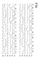
- FIG. 6 shows a time diagram for the various signals ES, VS, HS, ZS, UE and AS which occur in the converter circuit 18 or 20.
- the value of the signal output by the AND gate 23 is supplied from the flip-flop 24 with each positive edge of the auxiliary signal HS passed on to its output Q.
- the intermediate signal ZS is logic "1”
- the counter 22 is stopped.
- the counter 22 generates a carry (compare carry signal UE), with the occurrence of a pulse of the auxiliary signal HS, a logic "1" appears at the output Q of the flip-flop 24.
- the numbers below the signal AS represent the count of the counter 22 again.
- the "state-changed" comparison signal AS has, on average, a frequency which is lower by a factor of 2 than the frequency of the input signal ES. Also, the respective edges of input signal ES and “state-changed” comparison signal AS are offset. Due to this in the comparison signal caused irregularities or "state changes” the phase error is reduced in the transmission system.
- FIG. 7 An exemplary embodiment of a further comparator for a control loop is shown in FIG. 7.
- the comparator includes a first and second counters 25 and 26, first and second matching circuits 27 and 28, a subtracter 29 and a flip-flop 30.
- the first counter 25 receives at its clock input the first input signal and outputs at its count output as a comparison signal a sequence of Counts off.
- the first matching circuit 27 performs clock adjustment between the first input signal and the auxiliary signal HS.
- An embodiment of the matching circuit 27 or 28 is shown in FIG.
- the matching circuit 27 or 28 includes a first decoder for converting values coded by the dual code into values encoded according to the Gray code, two latches 32 and 33 and a second decoder 34 for converting values encoded according to the Gray code into values encoded after the dual code , After conversion of the values of the comparison signal coded according to the dual code into values coded according to the Gray code in the first decoder 31, an intermediate storage of the values output by the first decoder 31 is carried out in the buffer 32.
- the latch 32 may be formed as a register which receives the input signal at its clock input.
- the intermediate memory 33 which is likewise designed as a register and receives the auxiliary signal HS at its clock input, carries out an intermediate storage of the values output by the buffer 32.
- the output of the latch 33 is connected to the second decoder 34 which supplies values coded after the dual code after the conversion.
- the latches 32 and 33 serve to synchronize the values with the auxiliary signal HS.
- the count value often can not be buffered correctly. If, for example, a first bit position of the counter has already changed at the time of writing into the buffer memory 32, but a second bit position of the counter has not yet changed, this results in a wrongly entered count value. To minimize this error, the dual gray code conversion is performed.
- the Gray code is a one-step code that changes only one bit position on successive values.
- the values supplied by the matching circuit 27 are supplied to an input of the subtracter 29.
- the other input of the subtractor 29 receives values from the second matching circuit 28, which respectively receives count values from the second counter 26 and at the clock inputs as well as the first matching circuit 27 receives the second input signal and the auxiliary signal HS.
- the output values of the subtractor 29 are buffered in the flip-flop 30, which receives the auxiliary signal HS at its clock input.
- the matching circuits 27 and 28 perform state changes in the comparison signals supplied from the counters 25 and 26.
- the comparator of FIG. 7 can be used in the phase-locked loop of FIG. 3 or in the synchronizing circuit of FIG. 9 described below.
- the synchronizing circuit of FIG. 9, like the known synchronizing circuit of FIG. 3, includes a buffer memory 35 for latching incoming data of a signal, a timing recovery device 36 for generating a write clock signal ST, a write counter 37 for generating write addresses, a data analyzer 38 for Evaluation of pointer values, a read counter 39 for generating read addresses, a subtractor 40 forming a difference value, a low-pass filter 41, a stuffing decision-giving circuit 42, a multiplexing circuit 43 for forming the outgoing signal, a data generator 44 for controlling the reading counter 39 and the multiplexing circuit 43 and a phase locked loop 45 for generating the read clock signal LT.
- the phase-locked loop 45 receives control or synchronization information, for example from a management system used to control and monitor the transmission system.
- the new comparator 46 of FIG. 9 used in the synchronizing circuit includes, in addition to the writing counter 37 (first counter), the reading counter 39 (second counter) and the subtractor 40, two matching circuits 47 and 48.
- the matching circuit 47 receives the write addresses from the write counter 37 , the write clock signal ST and an auxiliary signal HS.
- the write address synchronized with the auxiliary signal HS is supplied to an input of the subtractor 40.
- the matching circuit 48 receives, in addition to the read clock signal LT and the auxiliary signal HS, also the read addresses from the read counter 39.
- the subtracter 40 receives synchronized read addresses supplied with the auxiliary signal HS.
- Both matching circuits 47 and 48 correspond to the matching circuit of FIG.
- the low pass filter 41 and the Stopfentscheidungsscrien 42 nor the auxiliary signal HS are supplied to the clocking.
- other switching elements can receive the auxiliary signal HS for timing.
- the read counter 39, the write counter 37, the matching circuits 47 and 48, the subtracter 40, the low-pass filter 41, the stuff decision circuit 42 and the data generator 44 constitute a control circuit for controlling the read-out operation of data from the buffer memory 35. Further, the low-pass filter 41, Stopfentscheidungsscrien 42 and the data generator 44, a controller.
- the synchronizing circuit shown in FIG. 9 can also be used in a preprocessing arrangement for clock adaptation and separate a postprocessing order for pointer evaluation.
- a preprocessing arrangement is known from DE-43 32 761 and is shown together with further switching elements in FIG.
- the pre-processing arrangement shown in Fig. 10 includes a buffer memory 49 receiving, for example, an STM-1 signal, a write counter 50 (first counter), a read counter 51 (second counter), a subtracter 52, a stuff decision circuit 53, an encoder 54, a frame evaluation circuit 55, a multiplexer 56, two matching circuits 57 and 58, two registers 59 and 60 and a low-pass filter 61.
- the write counter 50 which is formed as a modulo-4 counter, for example, receives the write clock signal ST and generates a write address with each clock.
- the write addresses generated after the one-step Gray code repeat themselves cyclically.
- The. Write addresses are supplied to the buffer memory 49 and the matching circuit 57, which receives the auxiliary signal HS at its clock input. Between the output of the matching circuit 57 and an input of the subtracter 52 is the register 59, which receives the read clock signal LT.
- the read counter 51 which may also be designed as a modulo-4 counter and receives the read clock signal LT, supplies the buffer memory 49 with read addresses.
- the reading counter 51 is still supplied from the stuffing decision circuit 53, a control signal SL.
- the control signal SL indicates a positive stuffing action
- the last-generated read address is again outputted (read counter 51 is stopped). If a negative stuffing action is specified in the control signal SL, the actually following read address is skipped.
- the sequence of read addresses except the buffer memory 49 and the matching circuit 58 is supplied, which receives the auxiliary signal HS at its clock input and as well as the matching circuit 57 consists of a buffer (register). Between matching circuit 58 and subtractor 52, another register 60 receiving read clock signal LT is inserted.
- the matching circuits 57 and 58 serve to adapt the write and read addresses to the auxiliary clock. Registers 59 and 60, in turn, adjust the addresses output by matching circuits 57 and 58 to read clock signal LT.
- the stuffing decision circuit 53 forms the control signal SL and, in addition to the read clock signal LT, receives an enable pulse F1 at a certain time. When the enable pulse FI is present, the stuffing decision is made.
- the stuff decision circuit 53 compares the value supplied from the subtractor 52 via the low-pass filter 61 with first and second thresholds. The first threshold value corresponds to a lower level of the buffer memory 49 and the second threshold value to an upper level of the buffer memory 49. If the value supplied by the subtracter 52 falls below the first threshold value, it must be negatively stuffed and the control signal SL generated by the stuffing decision circuit contains an indication of a negative value stuffing action. When the value supplied from the subtractor 52 exceeds the second threshold, the control signal SL is output from the stuff decision circuit 53 with a positive stuffing action.
- Negative must be stuffed when the frequency of the read clock signal LT is less than the frequency of the write clock signal ST is. If the frequency of the read clock signal LT is greater than the frequency of the write clock signal ST, positive stuffing is required.
- the frame of the outgoing STM-1 signal is shortened by one byte at a predetermined position and extended at a certain position in the outgoing signal at a positive stuffing operation. This is achieved by means of the read counter 51, which either outputs a read address twice or skips a read address when the control signal SL changes.
- the stuffing decision circuit 53 forms, together with the low-pass filter 61, the controller of the control circuit consisting of the writing counter 50, the reading counter 51, the adjusting circuits 57 and 58, the registers 59 and 60 and the subtracter 52.
- the control circuit controls the read counter-51.
- the enable pulse FI for the stuff decision circuit 53 is generated by the frame evaluation circuit 55 which receives the read clock signal LT and the data stream output from the buffer memory 49.
- Such frame evaluation circuit 55 detects the frame start of an STM-1 signal and counts the bytes of the STM-1 frame.
- a counter included in the frame evaluation circuit 55 reaches a count corresponding to the beginning of the predetermined range (first byte of the 5th line of the STM-1 frame or first B2 byte)
- the frame evaluation circuit 55 generates the enable pulse.
- a switching signal UI for the multiplexer 56 is generated by the frame evaluation circuit 55.
- the first input of the multiplexer 56 is connected to the output of the buffer memory 49 and the second input to the encoder 54, the control signal SL receives. Only during the presence of the switching signal UI, the second input of the multiplexer 56 is connected to its output. Otherwise, the first input of the multiplexer 12 is coupled to its output.
- the encoder 54 provides a codeword indicating whether there is a positive, negative or no stuffing action. This codeword is superimposed as a second B2 byte in the outgoing STM-1 signal by means of the multiplexer 56 and the frame evaluation circuit 55.
Landscapes
- Engineering & Computer Science (AREA)
- Computer Networks & Wireless Communication (AREA)
- Signal Processing (AREA)
- Synchronisation In Digital Transmission Systems (AREA)
- Time-Division Multiplex Systems (AREA)
Claims (14)
- Système de transmission avec une boucle de régulation comprenant :un comparateur pour comparer un premier signal d'entrée et un deuxième signal d'entrée et délivrer un signal de sortie qui est acheminé à la boucle de régulation,caractérisé par les caractéristiques suivantes :des moyens pour former un signal auxiliaire (HS) qui, en tant que signal d'horloge, est différent de la fréquence du premier signal d'entrée ;des moyens (18 ; 25, 27) pour former un premier signal de comparaison qui est dérivé du premier signal d'entrée, à savoira) par codage du premier signal d'entrée, une chaîne de circuits constituée de deux décodeurs (31, 34) et de deux mémoires intermédiaires (32, 33) à laquelle est acheminé le signal auxiliaire (HS) étant prévue oub) avec lequel les impulsions ou les pauses d'impulsion sont rallongées ou raccourcies, un circuit constitué de deux compteurs (21, 22), d'une porte ET (23) et d'une bascule (24) auquel est acheminé le signal auxiliaire (HS) étant prévu ouc) avec lequel les impulsions dans le premier signal d'entrée sont supprimées ou multipliées à des moments donnés prédéfinis par le signal auxiliaire (HS) ;des moyens (20 ; 26, 28) pour former un deuxième signal de comparaison qui correspond au deuxième signal d'entrée ou qui est dérivé du deuxième signal d'entrée etdes moyens (19 ; 29) pour combiner le premier et le deuxième signal de comparaison pour former le signal de sortie.
- Système de transmission selon la revendication 1, caractérisé en ce que le deuxième signal de comparaison est obtenu en codant le deuxième signal d'entrée, une chaîne de circuits constituée de deux décodeurs (31, 34) et de deux mémoires intermédiaires (32, 33) étant prévue ou avec lequel les impulsions ou les pauses d'impulsion sont rallongées ou raccourcies, un circuit constitué de deux compteurs (21, 22), d'une porte ET (23) et d'une bascule (24) auquel est acheminé le signal auxiliaire (HS) étant prévu ou alors les impulsions dans le deuxième signal d'entrée sont supprimées ou multipliées à des moments donnés prédéfinis par le signal auxiliaire (HS).
- Système de transmission selon la revendication 2, le comparateur comprenant :un premier compteur d'entrée (25),un premier circuit d'adaptation (27) relié avec celui-ci pour effectuer une adaptation de l'horloge entre le premier signal d'entrée et le signal auxiliaire (HS),un deuxième compteur d'entrée (26),un deuxième circuit d'adaptation (28) relié avec celui-ci pour effectuer une adaptation de l'horloge entre le deuxième signal d'entrée et le signal auxiliaire (HS) etun soustracteur (29) qui est relié avec la sortie du circuit d'adaptation (27, 28) correspondant et délivre le signal de sortie.
- Système de transmission selon la revendication 3, caractérisé en ce que le circuit d'adaptation (27 ; 28) correspondant contient une première mémoire intermédiaire (33), dont l'entrée d'horloge est prévue pour la réception du signal auxiliaire (HS), pour le stockage temporaire des valeurs acheminées.
- Système de transmission selon la revendication 3 ou 4, caractérisé en ce que
la boucle de régulation fait partie d'un circuit de synchronisation destiné à compenser les fluctuations de fréquence et/ou de phase entre un signal arrivant et un signal partant,
le premier compteur d'entrée (25) est réalisé sous la forme d'un compteur d'écriture (37) et sert à générer des adresses d'écriture pour des données à écrire dans une mémoire tampon (35) et que le deuxième compteur d'entrée (26) est réalisé sous la forme d'un compteur de lecture (39) et sert à générer des adresses de lecture pour des données à lire depuis la mémoire tampon (35) et que le soustracteur (29, 40) est prévu pour délivrer son signal de sortie à un régulateur (41, 42, 44) contenu dans la boucle de régulation et servant à commander le compteur de lecture (39). - Système de transmission selon la revendication 5, caractérisé en ce que
le régulateur contient un filtre passe-bas (41) recevant le signal de sortie du soustracteur (40), un circuit de décision de bouchon (42) et un générateur de données (44),
le circuit de décision de bouchon (42) est prévu pour interpréter les signaux de sortie du filtre passe-bas (41) et pour délivrer des valeurs de bouchon au générateur de données (44) et
le générateur de données (44) est prévu pour commander les actions de bouchon. - Système de transmission selon la revendication 5 ou 6, caractérisé en ce que
le circuit de synchronisation contient un analyseur de données (38) pour analyser les données arrivantes et pour commander le compteur d'écriture (37) . - Système de transmission selon la revendication 5, caractérisé en ce que
le régulateur est réalisé sous la forme d'un circuit de décision de bouchon (53) qui est prévu pour générer, au moins une fois pendant chaque trame du signal sortant, un signal de commande qui, si une valeur dérivée de la valeur de sortie du soustracteur (29, 52) est inférieure à une première valeur de seuil, indique une action de bouchon négative et qui, si la valeur dérivée de la valeur de sortie du soustracteur (29, 52) est supérieure à une deuxième valeur de seuil, laquelle est supérieure à la première valeur de seuil, indique une action de bouchon positive et
le compteur de lecture (39, 51) est prévu pour, pendant une plage prédéfinie de chaque trame du signal sortant, générer au moins une double adresse de lecture si le signal de commande indique une action de bouchon positive et sauter au moins une adresse de lecture si le signal de commande indique une action de bouchon négative. - Système de transmission selon l'une des revendications 4 à 7, caractérisé en ce que le circuit d'adaptation (27; 28) correspondant contient un premier décodeur (31) dont la sortie est connectée à l'entrée de la deuxième mémoire intermédiaire (33) et qui est prévu pour décoder les valeurs d'entrée reçues dans un code à une étape.
- Système de transmission selon la revendication 9, caractérisé en ce que
le premier décodeur (31) est prévu pour convertir en un code Gray les valeurs d'entrée codées en un code dual et
le circuit d'adaptation correspondant comprend une deuxième mémoire intermédiaire (32) dont la sortie est connectée à l'entrée de la première mémoire intermédiaire (33) pour le stockage temporaire des valeurs de sortie délivrées par le premier décodeur (31) et pour la réception à son entrée d'horloge d'un signal corrélé avec les valeurs acheminées et un deuxième décodeur (34) pour convertir en valeurs codées selon le code dual les valeurs de sortie de la première mémoire intermédiaire (33) codées selon le code Gray. - Système de transmission selon la revendication 1, caractérisé en ce que le comparateur (18, 19) englobe un premier circuit convertisseur (18) et un compteur de comparaison (19), le premier signal d'entrée et le signal auxiliaire (HS) étant acheminés au premier circuit convertisseur (18) pour former le premier signal de comparaison et le premier signal de comparaison pouvant être acheminé à l'entrée de validation du compteur de comparaison (19) et le deuxième signal de comparaison à l'entrée d'horloge du compteur de comparaison (19).
- Système de transmission selon la revendication 11, caractérisé en ce que
le comparateur (18, 19) contient un premier et un deuxième compteur (21, 22), une première bascule (24) et une porte ET (23),
le premier compteur (21) est prévu pour recevoir l'un des signaux d'entrée et pour délivrer un signal de comparaison unique d'une sortie à 1 bit du compteur (21),
la première bascule (24) est prévue pour recevoir le signal auxiliaire (HS) à son entrée d'horloge et pour recevoir le signal délivré par la porte ET (23) à son entrée de bascule, lequel représente une combinaison du signal de comparaison et d'un signal transmis du deuxième compteur (22) et
le deuxième compteur (22) est prévu pour recevoir le signal auxiliaire (HS) à son entrée d'horloge, pour recevoir le signal de sortie inversé de la première bascule (24) à son entrée de validation, pour délivrer le signal transmis de sa sortie transmission et pour délivrer un signal de comparaison unique d'une sortie à 1 bit du deuxième compteur (22). - Système de transmission selon la revendication 1, le comparateur (18 à 20) comprenant :- un premier circuit convertisseur (18) auquel sont acheminés le premier signal d'entrée et le signal auxiliaire (HS) et qui forme le premier signal de comparaison,- un deuxième circuit convertisseur (20) auquel sont acheminés le deuxième signal d'entrée et le signal auxiliaire (HS) et qui forme le deuxième signal de comparaison,- un compteur de comparaison (19) qui est prévu pour recevoir à son entrée de validation le premier signal de comparaison généré par le premier circuit convertisseur (18) et à son entrée d'horloge le deuxième signal d'entrée sous la forme d'un deuxième signal de comparaison, ou qui est prévu pour recevoir à son entrée de validation le premier signal d'entrée sous la forme d'un premier signal de comparaison et à son entrée d'horloge le deuxième signal de comparaison généré par le deuxième circuit convertisseur (20), ou qui est prévu pour recevoir à son entrée de validation le premier signal de comparaison généré par le premier circuit convertisseur (18) et à son entrée d'horloge le deuxième signal de comparaison généré par le deuxième circuit convertisseur (20).
- Système de transmission selon la revendication 13, caractérisé en ce que l'un des circuits de comparaison (18, 20) est prévu pour former un signal de comparaison unique à partir de l'un des signaux d'entrée, lequel présente au centre la même fréquence ou un multiple de la fréquence du signal de comparaison et dont les fronts sont en grande partie décalés par rapport aux fronts du signal de comparaison ou du signal de sortie.
Applications Claiming Priority (2)
| Application Number | Priority Date | Filing Date | Title |
|---|---|---|---|
| DE4437136A DE4437136A1 (de) | 1994-10-18 | 1994-10-18 | Übertragungssystem mit einem Regelkreis |
| DE4437136 | 1994-10-18 |
Publications (2)
| Publication Number | Publication Date |
|---|---|
| EP0708541A1 EP0708541A1 (fr) | 1996-04-24 |
| EP0708541B1 true EP0708541B1 (fr) | 2006-09-20 |
Family
ID=6531015
Family Applications (1)
| Application Number | Title | Priority Date | Filing Date |
|---|---|---|---|
| EP95202717A Expired - Lifetime EP0708541B1 (fr) | 1994-10-18 | 1995-10-10 | Système de transmission avec une boucle de commande |
Country Status (5)
| Country | Link |
|---|---|
| US (1) | US5859882A (fr) |
| EP (1) | EP0708541B1 (fr) |
| JP (1) | JPH08204666A (fr) |
| CN (1) | CN1129872A (fr) |
| DE (2) | DE4437136A1 (fr) |
Families Citing this family (21)
| Publication number | Priority date | Publication date | Assignee | Title |
|---|---|---|---|---|
| JPH10257034A (ja) * | 1997-03-12 | 1998-09-25 | Nec Corp | 無瞬断切替装置 |
| US6233629B1 (en) * | 1999-02-05 | 2001-05-15 | Broadcom Corporation | Self-adjusting elasticity data buffer with preload value |
| JP3703997B2 (ja) * | 1999-07-06 | 2005-10-05 | 沖電気工業株式会社 | 映像信号制御回路 |
| US6681272B1 (en) * | 1999-10-20 | 2004-01-20 | Applied Micro Circuits Corporation | Elastic store circuit with static phase offset |
| US6629251B1 (en) * | 1999-10-20 | 2003-09-30 | Applied Micro Circuits Corporation | Elastic store circuit with vernier clock delay |
| US6424189B1 (en) * | 2000-10-13 | 2002-07-23 | Silicon Integrated Systems Corporation | Apparatus and system for multi-stage event synchronization |
| AU2002251700A1 (en) * | 2000-12-20 | 2002-07-30 | Primarion, Inc. | Pll/dll dual loop data synchronization |
| AU2002235260A1 (en) * | 2000-12-20 | 2002-07-01 | Primarion, Inc. | Pll/dll dual loop data synchronization utilizing a granular fifo fill level indicator |
| US7447239B2 (en) * | 2002-09-19 | 2008-11-04 | Nortel Networks Limited | Transmission path monitoring |
| CN100334500C (zh) * | 2003-12-30 | 2007-08-29 | 财团法人资讯工业策进会 | 互动式3d场景照明方法及其系统 |
| US7546400B2 (en) * | 2004-02-13 | 2009-06-09 | International Business Machines Corporation | Data packet buffering system with automatic threshold optimization |
| US8281369B2 (en) * | 2008-03-12 | 2012-10-02 | Avaya Inc. | Method and apparatus for creating secure write-enabled web pages that are associated with active telephone calls |
| US8879464B2 (en) | 2009-01-29 | 2014-11-04 | Avaya Inc. | System and method for providing a replacement packet |
| US9525710B2 (en) * | 2009-01-29 | 2016-12-20 | Avaya Gmbh & Co., Kg | Seamless switch over from centralized to decentralized media streaming |
| US8238335B2 (en) | 2009-02-13 | 2012-08-07 | Avaya Inc. | Multi-route transmission of packets within a network |
| US7936746B2 (en) * | 2009-03-18 | 2011-05-03 | Avaya Inc. | Multimedia communication session coordination across heterogeneous transport networks |
| US20100265834A1 (en) * | 2009-04-17 | 2010-10-21 | Avaya Inc. | Variable latency jitter buffer based upon conversational dynamics |
| US8094556B2 (en) * | 2009-04-27 | 2012-01-10 | Avaya Inc. | Dynamic buffering and synchronization of related media streams in packet networks |
| US8553849B2 (en) | 2009-06-17 | 2013-10-08 | Avaya Inc. | Personal identification and interactive device for internet-based text and video communication services |
| US8800049B2 (en) * | 2009-08-26 | 2014-08-05 | Avaya Inc. | Licensing and certificate distribution via secondary or divided signaling communication pathway |
| JP5956284B2 (ja) * | 2012-08-15 | 2016-07-27 | Necネットワーク・センサ株式会社 | スタッフ同期制御回路及びスタッフ同期制御方法 |
Family Cites Families (18)
| Publication number | Priority date | Publication date | Assignee | Title |
|---|---|---|---|---|
| US5359605A (en) * | 1989-06-22 | 1994-10-25 | U.S. Philips Corporation | Circuit arrangement for adjusting the bit rates of two signals |
| DE3922897A1 (de) * | 1989-07-12 | 1991-01-17 | Philips Patentverwaltung | Stopfentscheidungsschaltung fuer eine anordnung zur bitratenanpassung |
| DE3942883A1 (de) * | 1989-12-23 | 1991-06-27 | Philips Patentverwaltung | Schaltungsanordnung zur bitratenanpassung |
| DE3942885A1 (de) * | 1989-12-23 | 1991-06-27 | Philips Patentverwaltung | Schaltungsanordnung zur bitratenanpassung |
| GB9012436D0 (en) * | 1990-06-04 | 1990-07-25 | Plessey Telecomm | Sdh rejustification |
| DE4027967A1 (de) * | 1990-09-04 | 1992-03-05 | Philips Patentverwaltung | Stopfentscheidungsschaltung fuer eine anordnung zur bitratenanpassung |
| DE4027968A1 (de) * | 1990-09-04 | 1992-03-05 | Philips Patentverwaltung | Schaltungsanordnung zur bitratenanpassung zweier digitaler signale |
| DE4108429A1 (de) * | 1991-03-15 | 1992-09-17 | Philips Patentverwaltung | Uebertragungssystem fuer die digitale synchrone hierarchie |
| DE4110933A1 (de) * | 1991-04-04 | 1992-10-08 | Philips Patentverwaltung | Uebertragungssystem fuer die synchrone digitale hierachie |
| US5268936A (en) * | 1991-07-08 | 1993-12-07 | At&T Bell Laboratories | Synchronous digital signal to asynchronous digital signal desynchronizer |
| FI95636C (fi) * | 1992-02-14 | 1996-02-26 | Nokia Telecommunications Oy | Desynkronisaattori ja menetelmä osoitinvärinän vaimentamiseksi desynkronisaattorissa |
| FI90484C (fi) * | 1992-06-03 | 1999-08-11 | Nokia Telecommunications Oy | Menetelmä ja laite synkronisessa digitaalisessa tietoliikennejärjestelmässä käytettävän elastisen puskurimuistin täyttöasteen valvomiseksi |
| ES2125942T3 (es) * | 1993-06-18 | 1999-03-16 | Cit Alcatel | Disposicion de circuito digital bloqueado en fase. |
| DE4326771A1 (de) * | 1993-08-10 | 1995-02-16 | Philips Patentverwaltung | Übertragungssystem |
| EP0645914A1 (fr) * | 1993-09-20 | 1995-03-29 | ALCATEL BELL Naamloze Vennootschap | Noeud d'un réseau de télécommunication |
| DE4332761A1 (de) * | 1993-09-25 | 1995-03-30 | Philips Patentverwaltung | Übertragungssystem mit einer Anpassungsschaltung |
| DE4425087A1 (de) * | 1994-07-15 | 1996-01-18 | Philips Patentverwaltung | Übertragungssystem |
| US5563891A (en) * | 1995-09-05 | 1996-10-08 | Industrial Technology Research Institute | Waiting time jitter reduction by synchronizer stuffing threshold modulation |
-
1994
- 1994-10-18 DE DE4437136A patent/DE4437136A1/de not_active Withdrawn
-
1995
- 1995-10-10 EP EP95202717A patent/EP0708541B1/fr not_active Expired - Lifetime
- 1995-10-10 DE DE59511066T patent/DE59511066D1/de not_active Expired - Lifetime
- 1995-10-10 US US08/541,384 patent/US5859882A/en not_active Expired - Lifetime
- 1995-10-17 JP JP7268719A patent/JPH08204666A/ja active Pending
- 1995-10-18 CN CN95116185.7A patent/CN1129872A/zh active Pending
Also Published As
| Publication number | Publication date |
|---|---|
| DE4437136A1 (de) | 1996-04-25 |
| CN1129872A (zh) | 1996-08-28 |
| JPH08204666A (ja) | 1996-08-09 |
| US5859882A (en) | 1999-01-12 |
| EP0708541A1 (fr) | 1996-04-24 |
| DE59511066D1 (de) | 2006-11-02 |
Similar Documents
| Publication | Publication Date | Title |
|---|---|---|
| EP0708541B1 (fr) | Système de transmission avec une boucle de commande | |
| DE69836157T2 (de) | Verfahren und Vorrichtung zum Demultiplexen digitaler Signalströme | |
| DE3107232C2 (fr) | ||
| DE69627849T2 (de) | Verteilung der synchronisation in einer synchronen optischen umgebung | |
| DE69131066T2 (de) | Anordnung zum extrahieren von asynchronen signalen | |
| EP0507385B1 (fr) | Système de transmission pour la hiérarchie numérique synchrone | |
| DE69634124T2 (de) | Digitaler desynchronisierer | |
| EP0475498B1 (fr) | Circuit d'adaption du débit binaire de deux signaux numériques | |
| DE69104721T2 (de) | Verfahren und anordnung für datensynchronisierung. | |
| DE69232057T2 (de) | Digitale schaltungen zur taktentflatterung mit minimalem zittern | |
| EP0503732A2 (fr) | Système de transmission pour la hiérarchie numérique synchrone | |
| DE69323071T2 (de) | Anordnung von digitalen Phasenregelschleifen | |
| DE69132247T2 (de) | Phasenverriegelte Schleifenanordnung | |
| EP0435383B1 (fr) | Circuit d'adaptation de débit binaire | |
| DE2838757A1 (de) | Schnittstellenschaltung fuer zeitmultiplexleitungen von nachrichtenvermittlungsanlagen | |
| DE69220267T2 (de) | Pulsstopfanlage | |
| DE19515344A1 (de) | Synchrones digitales Übertragungssystem | |
| DE69229668T2 (de) | Synchrone Schaltung | |
| DE69225186T2 (de) | Endstationssynchronisierungsanordnung in einem digitalen asynchronen Übertragungsnetz | |
| EP0645909B1 (fr) | Système de transmission avec un circuit d'adaption | |
| EP0085337B1 (fr) | Système de télécommunications numériques | |
| DE2846960C2 (de) | Multiplexgerät | |
| DE4415288A1 (de) | Verfahren zur Aufbereitung und Wiedergewinnung von Daten sowie Anordnung hierzu | |
| EP0404268B1 (fr) | Dispositif d'adaptation des débits de deux signaux | |
| EP1094610A1 (fr) | Boucle de verrouillage de phase numérique |
Legal Events
| Date | Code | Title | Description |
|---|---|---|---|
| PUAI | Public reference made under article 153(3) epc to a published international application that has entered the european phase |
Free format text: ORIGINAL CODE: 0009012 |
|
| AK | Designated contracting states |
Kind code of ref document: A1 Designated state(s): DE FR GB |
|
| 17P | Request for examination filed |
Effective date: 19961024 |
|
| RAP1 | Party data changed (applicant data changed or rights of an application transferred) |
Owner name: LUCENT TECHNOLOGIES INC. |
|
| 17Q | First examination report despatched |
Effective date: 19990107 |
|
| GRAP | Despatch of communication of intention to grant a patent |
Free format text: ORIGINAL CODE: EPIDOSNIGR1 |
|
| GRAS | Grant fee paid |
Free format text: ORIGINAL CODE: EPIDOSNIGR3 |
|
| GRAA | (expected) grant |
Free format text: ORIGINAL CODE: 0009210 |
|
| AK | Designated contracting states |
Kind code of ref document: B1 Designated state(s): DE FR GB |
|
| REG | Reference to a national code |
Ref country code: GB Ref legal event code: FG4D Free format text: NOT ENGLISH |
|
| REF | Corresponds to: |
Ref document number: 59511066 Country of ref document: DE Date of ref document: 20061102 Kind code of ref document: P |
|
| GBT | Gb: translation of ep patent filed (gb section 77(6)(a)/1977) |
Effective date: 20061101 |
|
| ET | Fr: translation filed | ||
| PLBE | No opposition filed within time limit |
Free format text: ORIGINAL CODE: 0009261 |
|
| STAA | Information on the status of an ep patent application or granted ep patent |
Free format text: STATUS: NO OPPOSITION FILED WITHIN TIME LIMIT |
|
| 26N | No opposition filed |
Effective date: 20070621 |
|
| REG | Reference to a national code |
Ref country code: GB Ref legal event code: 732E Free format text: REGISTERED BETWEEN 20131031 AND 20131106 |
|
| REG | Reference to a national code |
Ref country code: FR Ref legal event code: CD Owner name: ALCATEL-LUCENT USA INC. Effective date: 20131122 |
|
| PGFP | Annual fee paid to national office [announced via postgrant information from national office to epo] |
Ref country code: DE Payment date: 20131021 Year of fee payment: 19 Ref country code: GB Payment date: 20131021 Year of fee payment: 19 Ref country code: FR Payment date: 20131022 Year of fee payment: 19 |
|
| REG | Reference to a national code |
Ref country code: FR Ref legal event code: GC Effective date: 20140410 |
|
| REG | Reference to a national code |
Ref country code: FR Ref legal event code: RG Effective date: 20141015 |
|
| REG | Reference to a national code |
Ref country code: DE Ref legal event code: R119 Ref document number: 59511066 Country of ref document: DE |
|
| GBPC | Gb: european patent ceased through non-payment of renewal fee |
Effective date: 20141010 |
|
| PG25 | Lapsed in a contracting state [announced via postgrant information from national office to epo] |
Ref country code: GB Free format text: LAPSE BECAUSE OF NON-PAYMENT OF DUE FEES Effective date: 20141010 Ref country code: DE Free format text: LAPSE BECAUSE OF NON-PAYMENT OF DUE FEES Effective date: 20150501 |
|
| REG | Reference to a national code |
Ref country code: FR Ref legal event code: ST Effective date: 20150630 |
|
| PG25 | Lapsed in a contracting state [announced via postgrant information from national office to epo] |
Ref country code: FR Free format text: LAPSE BECAUSE OF NON-PAYMENT OF DUE FEES Effective date: 20141031 |