EP0705439B1 - Testvorrichtung sowie -verfahren für einen auf einer platine eingelöteten ic - Google Patents
Testvorrichtung sowie -verfahren für einen auf einer platine eingelöteten ic Download PDFInfo
- Publication number
- EP0705439B1 EP0705439B1 EP94919624A EP94919624A EP0705439B1 EP 0705439 B1 EP0705439 B1 EP 0705439B1 EP 94919624 A EP94919624 A EP 94919624A EP 94919624 A EP94919624 A EP 94919624A EP 0705439 B1 EP0705439 B1 EP 0705439B1
- Authority
- EP
- European Patent Office
- Prior art keywords
- collector
- voltage
- integrated circuit
- pin
- current
- Prior art date
- Legal status (The legal status is an assumption and is not a legal conclusion. Google has not performed a legal analysis and makes no representation as to the accuracy of the status listed.)
- Expired - Lifetime
Links
Images

Classifications
-
- G—PHYSICS
- G01—MEASURING; TESTING
- G01R—MEASURING ELECTRIC VARIABLES; MEASURING MAGNETIC VARIABLES
- G01R31/00—Arrangements for testing electric properties; Arrangements for locating electric faults; Arrangements for electrical testing characterised by what is being tested not provided for elsewhere
- G01R31/50—Testing of electric apparatus, lines, cables or components for short-circuits, continuity, leakage current or incorrect line connections
- G01R31/66—Testing of connections, e.g. of plugs or non-disconnectable joints
- G01R31/67—Testing the correctness of wire connections in electric apparatus or circuits
Definitions
- the invention relates to a test device of the type mentioned in the preambles of claims 1 to 3 and a test method of the type mentioned in the preambles of claims 8 to 10.
- Such a test device with the corresponding method is from the DE-C-41 10 551 known. It is used to determine parasitic transistors that are present in an IC and can be tapped from the outside via pins of the IC and that are composed of diodes of the IC that are formed against ground in the substrate of the IC. These diodes are parasitic diodes. The transistors formed therefrom are therefore referred to as parasitic transistors or lateral transistors.
- the transistor measurement takes place in the so-called emitter circuit, in which the emitter of the transistor is connected to the ground of the tester.
- the base of the transistor which corresponds to the GND pin (ground pin) of the IC, is not connected to ground, as is customary in ICs, but to a base voltage suitable for driving the transistor.
- Two IC signal pins are connected as collectors or emitters. The diodes between GND and the signal pins form the emitter and collector diodes of the transistor. The collector current is measured. This transistor to be determined is referred to below as a "test transistor".
- the advantage compared to older test methods, for example the node impedance measurement, is advantageous here, on complex boards with many ICs, of which many pins are connected in parallel, in particular in bus circuits, to make statements about the correct soldering of the pins.
- test transistors In the case of ICs implemented in bipolar technology (TTL logic), the existing test transistors can be determined very well in this way.
- TTL logic TTL logic
- CMOS technology which are becoming increasingly popular.
- Today's higher integrated ICs are almost exclusively manufactured using CMOS technology.
- CMOS ICs Even when measuring isolated ICs with open pins (that is to say in the unsoldered state), there are unresolved problems which have recently become known to experts under the keyword “background current”. If a test transistor is measured in a CMOS IC, currents result which are substantially higher than the currents expected by the test transistor. A current which is referred to below as an additional current and which is also referred to in the art as a "background current” obviously flows to the current flowing through the test transistor. This additional current depends very much on the manufacturing parameters of the IC, e.g. different manufacturers or different production batches.
- test transistors are connected in parallel due to parallel connections between pins of the IC, if one knows the current of a test transistor, one could infer the number of test transistors from the measured current of the parallel connection, since the test transistors of an IC usually have very similar properties. However, if the additional very high additional current flows, such statements about the number of test transistors lying in parallel can no longer be made.
- the object of the present invention is therefore to provide test devices and methods of the type mentioned at the outset which, even in the case of CMOS ICs, enable the determination of test transistors with high accuracy and in particular with high resolution with respect to the additional current.
- the invention is based on the knowledge that in the case of CMOS ICs when a test transistor is opened, that is to say a transistor with ground on a signal pin, base on GND and collector on another signal pin, a transistor which is referred to below as an additional transistor is always opened, and without other pins of the IC being in contact with the test device.
- the additional transistor is a transistor with a collector on the supply voltage pin V cc . This additional transistor is present in all ICs, ie in CMOS ICs and also in bipolar ICs.
- CMOS ICs In CMOS ICs, a parasitic diode with a forward direction from the signal pin to the supply voltage pin lies between each signal pin and the supply voltage pin V cc . If a collector voltage is applied to a signal pin in a CMOS IC, current flows to the supply voltage pin V cc and there applies a voltage which is somewhat lower but sufficient due to the diode in between, which is referred to below as the additional voltage.
- the collector current measured at the signal pin connected as a collector is therefore composed of the current that flows through the test transistor and the current that flows through the additional transistor via the said diode.
- the diode located between GND and V cc regularly has the unpleasant property that it has much higher transmission values than the diodes located between GND and signal pins and working as collector diodes.
- the additional transistor therefore usually has significantly higher current amplification values than all test transistors. If the sum of the current of the test transistor and the current of the additional transistor is measured when measuring the collector current of a test transistor, the portion of interest generated by the test transistor is very small compared to the total current, and it is therefore not possible to make any precise statements about the current and about the Make properties of the test transistor.
- the additional current flowing through the additional transistor is the current which is also referred to in the more recent literature as "background current".
- V cc of all ICs are connected in parallel.
- signal pins of several ICs are usually connected in parallel, particularly in the case of bus structures. If signal pins connected in parallel are used as emitters of test transistors to be measured, additional transistors are connected in parallel in several ICs and are opened when a test transistor is measured. Such high additional currents then result that the collector current of the test transistor to be determined can no longer be determined even with the highest precision test devices.
- the invention succeeds in separating the collector currents from test transistors and the additional currents, so that test transistors can be measured with high accuracy.
- the collector current of the test transistor is determined in a conventional manner, which results as the sum of the current through the actual test transistor and the current of the additional transistor.
- the additional voltage that occurs at the supply voltage pin via the diode connecting the signal pin as the collector and the supply voltage connection V cc is measured, and in a second step the collector of the test transistor is switched off and only the additional transistor is operated by applying the previously measured additional voltage and the one previously used base voltage.
- the additional transistor is therefore operated with the same parameters with which it was previously operated together with the test transistor.
- the additional current is measured and can now be subtracted from the previously measured collector current, which results in the corrected collector current which corresponds only to the current which flows through the test transistor alone. According to claim 4, this difference formation can advantageously be carried out automatically by the test device.
- the additional current can be determined with a test device according to claim 2 or the method according to claim 9 by first again, in a conventional manner, the test transistor is measured (including additional current), the additional voltage is determined at V cc and then, with the base and emitter switched off, only the previously used collector voltage is applied to the signal pin previously used as a collector and the previously measured additional voltage is applied to the supply voltage pin V cc .
- the additional current then flows through the diode existing between these pins and can be measured and then deducted from the previously determined collector current, advantageously automatically according to claim 5.
- an additional voltage of the same magnitude corresponding to the collector voltage applied to it can be applied to the supply voltage pin V cc , but from a separate voltage source.
- the diode between the signal pin connected as a collector and the supply voltage pin is now guarded. There is the same tension at both ends. So no current flows through the diode.
- the collector current of the test transistor and the additional current through the additional transistor come from different, separate voltage sources, so that the current associated therewith, ie the corrected collector current, can be determined directly at the collector of the test transistor.
- test transistor is measured with high precision. Statements can thus be made about individual differences between different test transistors present in an IC, and it is also possible to indicate how many these are in the case of several test transistors lying in parallel, i.e. whether e.g. one of three parallel test transistors is missing.
- the tester can be used to examine whether the contacted test transistor behaves like a transistor. For example, the current gain can be measured, a transistor characteristic curve can be traversed with several measurements, or another typical transistor property can be determined. If, after checking, it is certain that the contacted test transistor behaves like a transistor, then it is certain that the contacted pins are soldered correctly and that the internal connections of the pins in the IC are in order, that is, for example, they were not destroyed by excessive soldering temperatures.
- collector current can also simply measure the collector current with a measurement on a test transistor contacted with the tester and decide whether this collector current corresponds to the current expected by the respective test transistor at the given base and collector voltages.
- the normalized collector currents determined in the manner specified which thus indicate, for example, that the current for a test transistor is 1.2 times the mean value, are independent of manufacturer or batch fluctuations, since the current values of the individual test transistors change in exactly the same way as the mean values. If the normalized collector current for a measured test transistor is 1.2 times the mean value, this is the case regardless of whether the collector current is 50 ⁇ A for an IC from a manufacturer or 2 mA for an IC from another manufacturer.
- test transistors are used for standardization, each of which has the same type of pin for the collectors and emitters.
- a test transistor with an input pin I as a collector and an output pin O as an emitter therefore belongs to a group I - O
- a test transistor with an output pin O as a collector and an input pin I as an emitter belongs to a group O - I.
- Other groups are e.g. I - I, O - O or groups formed with other pin types, e.g. Enable pins or chip select pins.
- the mean values are formed only from such groups of test transistors that are very similar to one another, it is ensured that the mean values change with great accuracy in ICs from different manufacturers or from different batches like the collector currents of individual test transistors. It is also taken into account that the mean values of groups can change differently between different manufacturers or batches.
- a method is advantageous in which the normalized currents of all test transistors are first determined with a circuit board known to be faultless and then this table of normalized currents with the normalized currents of a circuit board to be tested determined on the corresponding test transistors be compared. By simply comparing the tables, a decision can be made about "good” or "error".
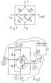
- CMOS IC shows the diode equivalent circuit diagram of a CMOS IC. To simplify the illustration, it is an IC with only two signal pins I and O (input, output). The supply voltage pin is labeled V cc . The ground pin of the IC is labeled GND. The diodes D 1 to D 5 that can be detected from outside during measurements between the pins are shown. These are bipolar diodes on the substrate of the IC, which are mostly parasitic diodes, i.e. not diodes that were deliberately arranged by the IC manufacturer, but diodes that result from the structure of the IC in the substrate with respect to ground .
- diodes are bipolar diodes with low internal resistance, through which high currents flow at low voltages, compared to the currents flowing in the highly complex MOSFET circuits (not shown) of the CMOS IC.
- the entire CMOS logic, not shown, of the IC can therefore be disregarded when considering currents flowing through the diodes D 1 to D 5 shown .
- all ohmic resistances or capacitances present in the IC are negligible, which are adapted to the low current level of the MOSFET circuits and are consequently negligible when considering currents through the diodes D 1 to D 5 .
- So-called clamping diodes provided for protection purposes on the signal pins also do not interfere, since they are mostly provided with series resistors and thus only allow comparatively low, ie insignificant, currents to flow.
- the MOSFET circuits can interfere if the supply voltage at V cc is so high that the MOSFETs open. On the input side, they are very high impedance, but they have very low output resistances that can interfere with the measurements.
- the pure diode equivalent circuit diagram of FIG. 1 therefore only applies if the supply voltage at V CC is below the voltage at which the field effect transistors of the CMOS logic open. This voltage is in the range of 2 volts in conventional CMOS ICs, but can be lower in modern ICs for battery-operated devices to a little less than 1 volt. This can be taken into account when applying the measuring voltages.
- the diodes D 1 and D 2 are arranged on the same substrate, they can form a test transistor based on GND, where I can form the collector and O the emitter or vice versa. 2 shows this in the usual transistor representation (circle). The base of the test transistor is at GND. D 2 forms the collector diode, D 1 forms the emitter diode.
- a tester T is provided, which is connected to the signal pin I with a collector output C, with a base connection B to the ground pin GND and with a ground connection E, which serves as an emitter, on the signal pin O.
- a ground connection E which serves as an emitter, on the signal pin O.
- it is indicated in addition to the pins I, GND and O that these are connected to the collector C, base B and emitter E.
- the emitter circuit of a transistor with an emitter is connected to ground.
- test transistor formed from D 2 and D 1 can be measured exactly in the case of bipolar ICs in which the diode D 5 is absent if V cc is not connected. In the case of CMOS ICs, however, this is not possible because the diode D 5 is present there.
- the test transistor formed from diodes D 1 and D 2 is a pnp transistor.
- the collector voltage is therefore positive compared to the emitter.
- the diode D 5 present in CMOS ICs is consequently in the forward direction, so that a voltage is present at V cc which corresponds to the collector voltage at I, reduced by the forward voltage of the diode D 5 .
- an additional transistor is formed, consisting of diodes D 3 and D 1 , with a collector at V cc , an emitter at O and a base at GND.
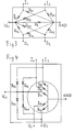
- FIG. 2 shows the circuit of FIG. 1 in a different representation.
- the transistor (circuit) has a common emitter diode D 1 and two collector diodes D 2 and D 3 .
- the collector of the test transistor is connected to I.
- the collector of the additional transistor is connected to V cc .
- the diode D 4 which has not yet been mentioned, can be disregarded in these considerations, since it is always in the reverse direction.
- the diode D 3 which serves as the collector diode of the additional transistor D 3 , D1
- D1 Unfortunately has the unpleasant property that a transistor formed with it has a considerably higher current gain than all test transistors which have a signal pin as a collector. Despite the somewhat lower collector voltage of the additional transistor this draws a much larger current.
- the current gain ⁇ is significantly higher, up to several orders of magnitude higher.
- Statements about the properties of the test transistor D 2 , D 1 cannot therefore be made because the current gain and thus the currents of the additional transistor D 3 , D 1 can fluctuate very greatly in ICs of the same type, for example between ICs different manufacturers or different production batches.
- test transistor D 2 If you want to measure the test transistor D 2, D 1, thus results by adding transistor D 3, D 1 a much higher background current that interferes with the measurement. In order to correct this, the tester T instructs an additional connection Z which is connected to V CC .
- the tester T is designed such that it can be switched over in two operating modes as follows:
- a collector voltage is applied to I with the collector connection C of the tester T.
- a base voltage is applied to GND.
- O of the IC is connected to the ground terminal E (emitter) of the tester.
- the collector current flowing through C is now determined. As already mentioned, this corresponds to the sum of the currents through the test transistor D 2 , D 1 and through the additional transistor D 3 , D 1 .
- the voltage at V cc is measured via the additional connection Z of the tester T.
- the tester T then switches to the second operating mode. With this the collector connection C is blocked. To V cc of the tester T is applied the previously measured in the first mode to V cc voltage across the auxiliary terminal Z. The base voltage at GND is selected at the same level as in the first operating mode.
- the currents determined at C and Z in the two operating modes are then divided from one another.
- the additional current of the additional transistor D 3 , D 1 is thus subtracted from the total collector current which results from the parallel connection of the test transistors D 2 , D 1 with the additional transistor D 3 , D 1 .
- the result is the corrected collector current of the test transistor D 2 , D 1 .
- this correction can be used to determine the isolated collector current of the test transistor D 2 , D 1 with very high accuracy.
- suitable measuring methods it is possible, for example, to compare the base current and collector current to determine the current gain ⁇ or by determining transistor characteristics when measuring several operating points, each with a corresponding correction of the additional current, i.e. measuring in both operating modes, the individual properties of the test transistor D 2 , D 1 determine with high precision.
- FIG. 2 it was explained that the pin I as the collector and the pin O as the emitter are connected for the transistor test. Since, as FIG. 1 shows, the diode arrangement is completely symmetrical with regard to the signal pins I and O, O can also be used as a collector and I as an emitter. If O is the collector of the test transistor, the now passing diode D 4 provides the connection to V cc . D 5 is blocked in this case.
- the transistor representation shown in FIG. 2 (with a circle), which shows a transistor with emitter diode D 1 and two parallel collector diodes D 2 and D 3 , would have to be represented differently for the case just described. It would then only be D 2 the emitter diode, while D 3 and D 1 form the parallel collector diodes.
- the base voltage at GND must also not be too high, since otherwise it pulls the voltage at V cc to a level that can be sufficient to open the CMOS logic.
- the test method described so far consists (see FIG. 2) of first connecting the signal pin O as the emitter and the grounding pin GND as the base and the signal pin I as the collector and measuring the current. Then I is de-energized and the additional voltage previously measured there is applied to V cc and the flowing additional current is measured. The additional current is then subtracted from the previously measured collector current. The corrected collector current results, which flows only through the test transistor D 2 , D 1 .
- the test transistor at pins O, GND and I is contacted with E, B and C and the collector current is determined.
- the additional voltage at V cc is determined.
- the second measuring step differs. A transistor is not measured here. O and GND are blocked. Only the previously used collector voltage is applied to I and the previously measured additional voltage to Vcc. Then exactly the current flows through the diode D 5 , which in the previous measurement fed the additional transistor D 3 , D 1 as a collector current. The additional current to be determined flows through the diode D 5 . This is measured at the connections C or Z of the tester T and can then be subtracted from the total collector current of both transistors previously measured at I, that is to say the test transistor including the additional transistor, in order to determine the true current of the test transistor D 2 , D 1 .
- test device Another alternative measurement method is possible with a different wiring of the test device as follows:
- the test transistor on pins I, GND and O is contacted with C, B and E, as shown in FIG. 2.
- the supply voltage pin V cc of the IC is contacted with the additional connection Z of the tester T, specifically with an additional voltage that corresponds exactly to the collector voltage at I.
- the additional connection Z of the tester T must be designed as a separate voltage source, so that the currents flowing at the connection C and the currents flowing at the connection Z can be determined separately from one another.
- I and Vcc have the same voltage.
- the diode D 5 is consequently de-energized. No current can flow through D 5 .
- the currents flowing through I and Vcc are therefore independent of one another.
- the collector current of the test transistor D 2 , D 1 can therefore be measured at I, that is to say at the collector terminal C of the tester T, independently of the additional current. A separate determination of the additional flow and subsequent difference formation can be omitted in this case.
- FIGS. 1 and 2 The IC shown in FIGS. 1 and 2 with only two signal pins is a great simplification for explanatory purposes.
- Commercially available ICs normally have significantly more signal pins. With modern, highly integrated ICs, the number of signal pins can go well over 100.
- FIGS. 3 and 4 an IC with four signal pins is shown in FIGS. 3 and 4 in a corresponding representation, as in FIGS. 1 and 2, which in any way one or Outputs can be. In the illustration, they are designated I 1 , I 2 , O 1 and O 2 .
- the bipolar diodes are shown in FIG. 3, with a numbering corresponding to that in FIG. 1, each with a second index number which refers to the pin. But there is only one diode D 3 between V cc and GND. Each signal pin is connected to a diode to GND and V cc by a diode. Several test transistors can thus be tapped, based on GND, collector on one of the signal pins and emitter on any of the other signal pins.
- Test transistors is always an additional transistor in parallel with the collector at Vcc and power supply via the lying of the connected as a collector signal pins to V cc diode.
- the transistor representation of FIG. 4 results with the transistor shown in a circle, which has the collector diodes D 22 , D 21 and D 3 and the emitter diodes D 11 and D 12 and which has the common base at GND.
- Fig. 3 shows that here again the signal pins I 1 , I 2 , O 1 and O 2 are connected completely identically to diodes. It is not necessary to always connect the collector of a transistor to an I pin and the emitter to an O pin. A transistor can also be formed, for example, between O 1 and O 2 , in which case the diodes D 11 and D 12 then form the collector or emitter diode of a transistor. The transistor representation of FIG. 4 is then to be redrawn accordingly. However, the use of only input pins I as a collector and only of output pins O as an emitter can be advantageous, since then all test transistors that can be formed have mutually similar values.
- FIG. 5 shows, in order to clarify a real test situation, two ICs in the representation according to FIG. 4, but with five signal pins each.
- the Both ICs are soldered onto a circuit board (not shown), that is to say electrically connected with their pins to conductor tracks.
- the signal pins of the two ICs shown are numbered above and below in the illustration.
- the conductor tracks with which the pins are connected are accordingly labeled with the letters "L".
- the signal pin I 1 of the left IC is individually connected to a conductor track LI 1 .
- the signal pin I 2 of the left IC and the signal pin I 5 of the right IC are connected to a conductor track LI 2.5 .
- the signal pin I 3 of the left IC is connected to a conductor track LI 3,6 together with a signal pin I 6 of the right IC.
- the signal pin I 4 of the right IC is individually connected to a conductor track LI 4 .
- the signal pin O of the left IC and the signal pin O 3 of the right IC are connected together to an interconnect LO 1,3 .
- the signal pin 2 O of the left ICs is connected with the signal pin of the right Ics O 4 to a conductor track LO 2.4 V cc and GND of the two signal pins are connected to common conductor paths LV cc and LGND.
- the conductor tracks are contacted at their contacts shown at the right end in FIG. 5.
- the LGND conductor track is always contacted with B since the base of the test transistors to be measured is always connected to GND.
- Z is always on LV cc .
- C and E can be connected to any of the interconnects connected to signal pins.
- C is connected to the conductor track LI 1 and E to the conductor track LO 2.4 .
- This is a favorably chosen example because only an isolated signal pin I 1 is connected to the collector connection C of the tester. So only the test transistor formed with the diode D 21 of the left IC as a collector diode is connected. However, this is due to the supply via the diode D 51, the additional transistor D 3 , D 11 in the left IC and since O 2 is connected to O 4 and V cc of both ICs are connected, the corresponding additional transistor in the right IC.
- the collector current at I 1 which is very weak, would be completely superimposed by the background current of the two additional transistors in the two ICs, which are in parallel, and could not be recognized.
- the tester T shown in FIG. 2 is connected with its additional connection to LV cc and carries out the measurements described above in which it can determine the collector current of the test transistor with collector at I 1 independently of the additional current of the two additional transistors in the two ICs shown .
- the properties of the test transistor formed with collector at I 1 can be measured. be measured exactly, and it can be determined whether this transistor is really connected fully functional. If this is the case, the result is that the pins of the IC involved, that is to say I 1 and O 2, are correctly contacted, that is to say are correctly soldered to the associated conductor tracks.
- test transistors are preferably used, the collector or emitter of which is alone connected to a conductor track.
- Pin I 4 can therefore preferably be used as a collector in the right IC.
- the result is a test transistor with a double collector, that is to say also with a double current.
- both collectors at I 2 and I 5 are correctly contacted that the double collector formed from I 2 and I 5 gives twice the collector current than when measuring the test transistors with a collector at I 1 or at I 4 .
- signal pin I 4 is also possible, for example, to use signal pin I 4 as a collector and signal pin I 5 as an emitter in the IC shown on the right. Then a statement about the correct contacting of these two signal pins is possible.
- I 1 As a collector and O 1 as an emitter, i.e. when E is connected to LO 1.3 , a statement is made about the correct contacting of O 1 . If I 1 is used as collector O 2 when I 1 is connected to E via LO 2.4 , this provides information about the correct contacting of O 2 . A corresponding procedure can be used to check O 3 and O 4 using I 4 as a collector.
- the corrected collector currents can be measured on all test transistors that can be formed, that is, the currents that only flow through the respective test transistor.
- Typical transistor properties such as current amplification or transistor characteristics, can be determined in order to decide whether the contacted pins are really connected to the conductor tracks when the tester T is connected to a specific test transistor will. The statement can then be made as to whether a correctly functioning transistor has actually been contacted. If this is the case, it is ensured that the relevant pins are correctly connected to the conductor tracks.
- collector current of a test transistor in a simple measurement and to check whether the measured collector current corresponds to the current to be expected from such a test transistor at the applied base and collector voltages. Since the collector currents of test transistors of an IC type can vary greatly among ICs from different manufacturers or from different production batches, this is not readily possible. For example, when measuring the corrected collector current of the test transistor connected in FIG. 5 from I 1 as a collector and O 1 as an emitter, a collector current of 10 mA can flow at an IC from one manufacturer, but with the same test transistor of the same IC type from another manufacturer but when applied the same base and collector voltages, a collector current of, for example, only 10 ⁇ A.
- the collector current of 10 ⁇ A is the correct collector current for an IC of the second manufacturer or whether an IC from the first manufacturer, in which the collector current should be 10 mA, the measured value is much too low and indicates a defect.
- test transistors with an input pin as a collector and an output pin as an emitter in the mean value of their collector currents can change differently than test transistors in a group with an output pin as a collector and an input pin as an emitter. Therefore, the collector currents of the test transistors are advantageously compared with the mean values of the corresponding group of test transistors in which collectors and emitters are of the same pin type.
- the pin types are usually before input pins, output pins, enable pins, chip select pins etc.
- test transistors are therefore measured with the tester with regard to their corrected collector currents, it being possible to examine all five pins I 1 , I 2 , I 3 , O 1 and O 2 by measuring four test transistors. These are the following test transistors, each of which is given the notation "collector-emitter", that is to say the transistors I 1 - O 1 , I 1 - O 2 , I 3 - I 1 and I 2 - I 1 .
- a measurement result is given in Table 1 below.
- the first column of the table indicates which pin is connected as a collector.
- the second column indicates which pin is connected as an emitter.
- the corrected collector current is given in the third column.
- the fourth column contains the mean value of the collector currents and the last column for each test transistor contains the collector current normalized with respect to the mean value, i.e. the ratio of the collector current to the mean value.
- the table is divided into two groups.
- the upper group I - O contains two test transistors, each of which has an I pin on the collector and the emitter is an o-pin.
- the second group I - I contains two test transistors, in which both the collector and the emitter are an I pin.
- Table 1 An IC from manufacturer A is examined in Table 1.
- the collector current is given for each transistor. This is an IC that has very low collector currents in the ⁇ A range from this manufacturer.
- the mean values for the two groups are given, and the normalized values are 0.93, 1.06, 0.90 and 1.09 for the four measured test transistors from top to bottom.
- Table 1 Manufacturer A collector Emitter Collector current Average normalized value Group I - O I 1 O 1 20 ⁇ A 0.93 21.5 ⁇ A I 1 0 2 23 ⁇ A 1.06 Group I - I I 3 I 1 10 ⁇ A 0.90 11 ⁇ A I 2 I 1 12 ⁇ A 1.09
- a board that is found to be good can be measured, and for all measured test transistors of the various ICs, they are divided according to the groups described above, as in the table 1 or 2 specified, the standardized values of the test transistors determined and stored in a table.
- the boards to be tested are then tested and the standardized values of the respective test transistors are compared with the standardized values of the corresponding test transistors of the gut board.
- Table 1 with Table 2 shows, errors can be recognized very precisely, regardless of whether the IC assembly was carried out with ICs from the same or different production batches or manufacturers.
Landscapes
- Physics & Mathematics (AREA)
- General Physics & Mathematics (AREA)
- Testing Of Individual Semiconductor Devices (AREA)
- Tests Of Electronic Circuits (AREA)
- Electric Connection Of Electric Components To Printed Circuits (AREA)
Applications Claiming Priority (3)
| Application Number | Priority Date | Filing Date | Title |
|---|---|---|---|
| DE4319710A DE4319710C1 (de) | 1993-06-15 | 1993-06-15 | Testverfahren für einen auf einer Platine eingelöteten IC und Testvorrichtung zum Durchführen des Testverfahrens |
| DE4319710 | 1993-06-15 | ||
| PCT/EP1994/001902 WO1994029738A1 (de) | 1993-06-15 | 1994-06-11 | Testvorrichtung sowie -verfahren für einen auf einer platine eingelöteten ic |
Publications (2)
| Publication Number | Publication Date |
|---|---|
| EP0705439A1 EP0705439A1 (de) | 1996-04-10 |
| EP0705439B1 true EP0705439B1 (de) | 1997-09-03 |
Family
ID=6490332
Family Applications (1)
| Application Number | Title | Priority Date | Filing Date |
|---|---|---|---|
| EP94919624A Expired - Lifetime EP0705439B1 (de) | 1993-06-15 | 1994-06-11 | Testvorrichtung sowie -verfahren für einen auf einer platine eingelöteten ic |
Country Status (13)
| Country | Link |
|---|---|
| US (1) | US6188235B1 (zh) |
| EP (1) | EP0705439B1 (zh) |
| JP (1) | JPH08511345A (zh) |
| KR (1) | KR960703232A (zh) |
| CN (1) | CN1044644C (zh) |
| AT (1) | ATE157776T1 (zh) |
| AU (1) | AU686639B2 (zh) |
| CA (1) | CA2164415A1 (zh) |
| DE (2) | DE4319710C1 (zh) |
| DK (1) | DK0705439T3 (zh) |
| ES (1) | ES2107236T3 (zh) |
| TW (1) | TW249843B (zh) |
| WO (1) | WO1994029738A1 (zh) |
Families Citing this family (9)
| Publication number | Priority date | Publication date | Assignee | Title |
|---|---|---|---|---|
| US6720774B2 (en) * | 2002-07-29 | 2004-04-13 | Sun Microsystems, Inc. | Interchangeable fan control board with fault detection |
| GB2394780B (en) * | 2002-10-29 | 2006-06-14 | Ifr Ltd | A method of and apparatus for testing for integrated circuit contact defects |
| KR100565326B1 (ko) * | 2004-05-25 | 2006-03-30 | 엘지전자 주식회사 | 이동통신 단말기의 엘씨디 컨넥터 체크 장치 |
| US7279907B2 (en) * | 2006-02-28 | 2007-10-09 | Freescale Semiconductor, Inc. | Method of testing for power and ground continuity of a semiconductor device |
| DE102008020667A1 (de) * | 2008-04-24 | 2010-05-20 | Continental Automotive Gmbh | Verfahren zur Fehlerüberwachung an einem Beleuchtungsausgang eines Kraftfahrzeuges |
| CN101571570B (zh) * | 2008-04-29 | 2013-05-22 | 京元电子股份有限公司 | 集成电路连续性测试方法及集成电路接触电阻的测量方法 |
| CN101825681B (zh) * | 2010-04-29 | 2013-07-31 | 上海宏力半导体制造有限公司 | 一种双极型晶体管电流放大系数测量方法 |
| RU173641U1 (ru) * | 2017-03-27 | 2017-09-04 | Закрытое акционерное общество "ГРУППА КРЕМНИЙ ЭЛ" | Тестовый планарный p-n-p транзистор |
| CN107424549B (zh) * | 2017-09-28 | 2020-04-17 | 京东方科技集团股份有限公司 | 阈值电压漂移的检测方法和装置 |
Family Cites Families (5)
| Publication number | Priority date | Publication date | Assignee | Title |
|---|---|---|---|---|
| US4779043A (en) * | 1987-08-26 | 1988-10-18 | Hewlett-Packard Company | Reversed IC test device and method |
| US5124660A (en) * | 1990-12-20 | 1992-06-23 | Hewlett-Packard Company | Identification of pin-open faults by capacitive coupling through the integrated circuit package |
| US5254953A (en) * | 1990-12-20 | 1993-10-19 | Hewlett-Packard Company | Identification of pin-open faults by capacitive coupling through the integrated circuit package |
| DE4110551C1 (zh) * | 1991-03-30 | 1992-07-23 | Ita Ingenieurbuero Fuer Testaufgaben Gmbh, 2000 Hamburg, De | |
| JP3157683B2 (ja) * | 1994-08-30 | 2001-04-16 | 株式会社 沖マイクロデザイン | 半導体集積回路の静止時電流測定法、半導体集積回路 |
-
1993
- 1993-06-15 DE DE4319710A patent/DE4319710C1/de not_active Expired - Fee Related
-
1994
- 1994-06-11 AU AU70715/94A patent/AU686639B2/en not_active Ceased
- 1994-06-11 WO PCT/EP1994/001902 patent/WO1994029738A1/de active IP Right Grant
- 1994-06-11 EP EP94919624A patent/EP0705439B1/de not_active Expired - Lifetime
- 1994-06-11 CA CA002164415A patent/CA2164415A1/en not_active Abandoned
- 1994-06-11 JP JP7501337A patent/JPH08511345A/ja active Pending
- 1994-06-11 US US08/557,039 patent/US6188235B1/en not_active Expired - Lifetime
- 1994-06-11 CN CN94192444A patent/CN1044644C/zh not_active Expired - Fee Related
- 1994-06-11 AT AT94919624T patent/ATE157776T1/de active
- 1994-06-11 ES ES94919624T patent/ES2107236T3/es not_active Expired - Lifetime
- 1994-06-11 DE DE59403978T patent/DE59403978D1/de not_active Expired - Lifetime
- 1994-06-11 DK DK94919624.0T patent/DK0705439T3/da active
- 1994-06-11 KR KR1019950705708A patent/KR960703232A/ko not_active Application Discontinuation
- 1994-09-02 TW TW083108101A patent/TW249843B/zh active
Also Published As
| Publication number | Publication date |
|---|---|
| AU686639B2 (en) | 1998-02-12 |
| ES2107236T3 (es) | 1997-11-16 |
| KR960703232A (ko) | 1996-06-19 |
| TW249843B (zh) | 1995-06-21 |
| CN1125482A (zh) | 1996-06-26 |
| AU7071594A (en) | 1995-01-03 |
| CA2164415A1 (en) | 1994-12-22 |
| CN1044644C (zh) | 1999-08-11 |
| JPH08511345A (ja) | 1996-11-26 |
| DK0705439T3 (da) | 1998-04-14 |
| WO1994029738A1 (de) | 1994-12-22 |
| ATE157776T1 (de) | 1997-09-15 |
| DE59403978D1 (de) | 1997-10-09 |
| DE4319710C1 (de) | 1994-09-29 |
| US6188235B1 (en) | 2001-02-13 |
| EP0705439A1 (de) | 1996-04-10 |
Similar Documents
| Publication | Publication Date | Title |
|---|---|---|
| EP0507168B1 (de) | Verfahren zum Testen von auf Platinen eingelöteten integrierten Halbleiterschaltkreisen und Verwendung eines Transistortesters für dieses Verfahren | |
| DE10191490B4 (de) | Verfahren und Vorrichtung zur Defektanalyse von integrierten Halbleiterschaltungen | |
| EP0523594B1 (de) | Verfahren zur Korpuskularstrahl-Prüfung von Substraten für Flüssigkeitskristallanzeigen (LCD) | |
| DE69733789T2 (de) | Hochauflösendes Stromversorgungsprüfsystem | |
| DE4417573C2 (de) | Testanordnung für Kurzschlußtests auf einer Leiterplatte und Verfahren zum Testen der Verbindung einer Mehrzahl von Knoten auf einer Leiterplatte unter Verwendung dieser Testanordnung | |
| DE2854549C2 (zh) | ||
| DE102007025001B4 (de) | Verfahren zum Testen einer Messbrücke, Messbrückenanordnung, Testanordnung zum Testen einer Messbrücke, Verfahren zum Herstellen einer getesteten Messbrückenanordnung und Computerprogramm | |
| DE102005016127B4 (de) | Sensorsystem | |
| EP0705439B1 (de) | Testvorrichtung sowie -verfahren für einen auf einer platine eingelöteten ic | |
| DE4017617C2 (de) | Spannungserzeugungsschaltung mit geringer Leistungsaufnahme und stabiler Ausgangsspannung bei kleiner Schaltkreisfläche | |
| DE2504076A1 (de) | Anordnung und verfahren zur kontaktpruefung von halbleiterschaltungen | |
| EP0203535B1 (de) | Verfahren zur Simulation eines Fehlers in einer logischen Schaltung und Schaltungsanordnung zur Durchführung desselben | |
| DE112004002703T5 (de) | Treiberschaltkreis | |
| DE19527487C1 (de) | Schaltungsanordnung zum Prüfen der Funktionsfähigkeit einer Stromüberwachungsschaltung für einen Leistungstransistor | |
| EP0733910B1 (de) | Platine mit eingebauter Kontaktfühlerprüfung für integrierte Schaltungen | |
| DE19714941A1 (de) | Meßkarte und Ein/Ausgang-Anschlußtestsystem unter Verwendung derselben | |
| DE10341836B4 (de) | Testvorrichtung zum Testen von elektrischen Schaltungen sowie Verfahren zum parallelen Testen von elektrischen Schaltungen | |
| DE19528733C1 (de) | Integrierte Schaltung | |
| EP0729034A2 (de) | Prüfschaltung und Prüfverfahren zur Funktionsprüfung von elektronischen Schaltungen | |
| DE4309842C1 (de) | Verfahren zum Testen von Platinen und Vorrichtung zur Durchführung des Verfahrens | |
| DE10214885C1 (de) | Verfahren und Teststruktur zur Bestimmung von Widerstandwerten an mehreren zusammengeschalteten Widerständen in einer integrierten Schaltung | |
| EP1266404B1 (de) | Test-schaltungsanordnung und verfahren zum testen einer vielzahl von elektrischen komponenten | |
| DE102021001093B4 (de) | Eingebundenes Testinstrument für Hochgeschwindigkeitsschnittstellen | |
| DE102008062929B4 (de) | Elektronische Vorrichtung und Verfahren zur Leitungsprüfung | |
| DE102021118672A1 (de) | Testsystem und -verfahren für chip-entkopplungskondensatorschaltungen |
Legal Events
| Date | Code | Title | Description |
|---|---|---|---|
| PUAI | Public reference made under article 153(3) epc to a published international application that has entered the european phase |
Free format text: ORIGINAL CODE: 0009012 |
|
| 17P | Request for examination filed |
Effective date: 19951129 |
|
| AK | Designated contracting states |
Kind code of ref document: A1 Designated state(s): AT BE CH DE DK ES FR GB IE IT LI NL PT SE |
|
| 17Q | First examination report despatched |
Effective date: 19960322 |
|
| GRAG | Despatch of communication of intention to grant |
Free format text: ORIGINAL CODE: EPIDOS AGRA |
|
| GRAH | Despatch of communication of intention to grant a patent |
Free format text: ORIGINAL CODE: EPIDOS IGRA |
|
| GRAH | Despatch of communication of intention to grant a patent |
Free format text: ORIGINAL CODE: EPIDOS IGRA |
|
| GRAA | (expected) grant |
Free format text: ORIGINAL CODE: 0009210 |
|
| AK | Designated contracting states |
Kind code of ref document: B1 Designated state(s): AT BE CH DE DK ES FR GB IE IT LI NL PT SE |
|
| REF | Corresponds to: |
Ref document number: 157776 Country of ref document: AT Date of ref document: 19970915 Kind code of ref document: T |
|
| ITF | It: translation for a ep patent filed |
Owner name: SPADINI MARUSCO |
|
| REG | Reference to a national code |
Ref country code: CH Ref legal event code: EP |
|
| REG | Reference to a national code |
Ref country code: CH Ref legal event code: NV Representative=s name: WILLIAM BLANC & CIE CONSEILS EN PROPRIETE INDUSTRI |
|
| REF | Corresponds to: |
Ref document number: 59403978 Country of ref document: DE Date of ref document: 19971009 |
|
| ET | Fr: translation filed | ||
| REG | Reference to a national code |
Ref country code: ES Ref legal event code: FG2A Ref document number: 2107236 Country of ref document: ES Kind code of ref document: T3 |
|
| REG | Reference to a national code |
Ref country code: PT Ref legal event code: SC4A Free format text: AVAILABILITY OF NATIONAL TRANSLATION Effective date: 19970917 |
|
| GBT | Gb: translation of ep patent filed (gb section 77(6)(a)/1977) |
Effective date: 19971204 |
|
| REG | Reference to a national code |
Ref country code: IE Ref legal event code: FG4D Free format text: 76258 |
|
| REG | Reference to a national code |
Ref country code: DK Ref legal event code: T3 |
|
| PG25 | Lapsed in a contracting state [announced via postgrant information from national office to epo] |
Ref country code: IE Free format text: LAPSE BECAUSE OF NON-PAYMENT OF DUE FEES Effective date: 19980605 |
|
| PGFP | Annual fee paid to national office [announced via postgrant information from national office to epo] |
Ref country code: PT Payment date: 19980615 Year of fee payment: 5 |
|
| PGFP | Annual fee paid to national office [announced via postgrant information from national office to epo] |
Ref country code: DK Payment date: 19980623 Year of fee payment: 5 |
|
| PGFP | Annual fee paid to national office [announced via postgrant information from national office to epo] |
Ref country code: AT Payment date: 19980629 Year of fee payment: 5 |
|
| PGFP | Annual fee paid to national office [announced via postgrant information from national office to epo] |
Ref country code: NL Payment date: 19980630 Year of fee payment: 5 |
|
| REG | Reference to a national code |
Ref country code: IE Ref legal event code: FD4D Ref document number: 76258 Country of ref document: IE |
|
| PGFP | Annual fee paid to national office [announced via postgrant information from national office to epo] |
Ref country code: CH Payment date: 19980706 Year of fee payment: 5 |
|
| PLBE | No opposition filed within time limit |
Free format text: ORIGINAL CODE: 0009261 |
|
| STAA | Information on the status of an ep patent application or granted ep patent |
Free format text: STATUS: NO OPPOSITION FILED WITHIN TIME LIMIT |
|
| PGFP | Annual fee paid to national office [announced via postgrant information from national office to epo] |
Ref country code: BE Payment date: 19980714 Year of fee payment: 5 |
|
| 26N | No opposition filed | ||
| PGFP | Annual fee paid to national office [announced via postgrant information from national office to epo] |
Ref country code: SE Payment date: 19990609 Year of fee payment: 6 |
|
| PG25 | Lapsed in a contracting state [announced via postgrant information from national office to epo] |
Ref country code: AT Free format text: LAPSE BECAUSE OF NON-PAYMENT OF DUE FEES Effective date: 19990611 |
|
| PGFP | Annual fee paid to national office [announced via postgrant information from national office to epo] |
Ref country code: ES Payment date: 19990614 Year of fee payment: 6 |
|
| PGFP | Annual fee paid to national office [announced via postgrant information from national office to epo] |
Ref country code: GB Payment date: 19990616 Year of fee payment: 6 |
|
| PGFP | Annual fee paid to national office [announced via postgrant information from national office to epo] |
Ref country code: FR Payment date: 19990628 Year of fee payment: 6 |
|
| PG25 | Lapsed in a contracting state [announced via postgrant information from national office to epo] |
Ref country code: LI Free format text: LAPSE BECAUSE OF NON-PAYMENT OF DUE FEES Effective date: 19990630 Ref country code: DK Free format text: LAPSE BECAUSE OF NON-PAYMENT OF DUE FEES Effective date: 19990630 Ref country code: CH Free format text: LAPSE BECAUSE OF NON-PAYMENT OF DUE FEES Effective date: 19990630 Ref country code: BE Free format text: LAPSE BECAUSE OF NON-PAYMENT OF DUE FEES Effective date: 19990630 |
|
| BERE | Be: lapsed |
Owner name: INGENIEURBURO FUR TESTAUFGABEN G.M.B.H. ITA Effective date: 19990630 |
|
| PG25 | Lapsed in a contracting state [announced via postgrant information from national office to epo] |
Ref country code: PT Free format text: LAPSE BECAUSE OF NON-PAYMENT OF DUE FEES Effective date: 19991231 |
|
| PG25 | Lapsed in a contracting state [announced via postgrant information from national office to epo] |
Ref country code: NL Free format text: LAPSE BECAUSE OF NON-PAYMENT OF DUE FEES Effective date: 20000101 |
|
| REG | Reference to a national code |
Ref country code: CH Ref legal event code: PL |
|
| NLV4 | Nl: lapsed or anulled due to non-payment of the annual fee |
Effective date: 20000101 |
|
| REG | Reference to a national code |
Ref country code: DK Ref legal event code: EBP |
|
| REG | Reference to a national code |
Ref country code: PT Ref legal event code: MM4A Free format text: LAPSE DUE TO NON-PAYMENT OF FEES Effective date: 19991231 |
|
| PG25 | Lapsed in a contracting state [announced via postgrant information from national office to epo] |
Ref country code: GB Free format text: LAPSE BECAUSE OF NON-PAYMENT OF DUE FEES Effective date: 20000611 |
|
| PG25 | Lapsed in a contracting state [announced via postgrant information from national office to epo] |
Ref country code: SE Free format text: LAPSE BECAUSE OF NON-PAYMENT OF DUE FEES Effective date: 20000612 Ref country code: ES Free format text: THE PATENT HAS BEEN ANNULLED BY A DECISION OF A NATIONAL AUTHORITY Effective date: 20000612 |
|
| GBPC | Gb: european patent ceased through non-payment of renewal fee |
Effective date: 20000611 |
|
| EUG | Se: european patent has lapsed |
Ref document number: 94919624.0 |
|
| PG25 | Lapsed in a contracting state [announced via postgrant information from national office to epo] |
Ref country code: FR Free format text: LAPSE BECAUSE OF NON-PAYMENT OF DUE FEES Effective date: 20010228 |
|
| REG | Reference to a national code |
Ref country code: FR Ref legal event code: ST |
|
| REG | Reference to a national code |
Ref country code: ES Ref legal event code: FD2A Effective date: 20020204 |
|
| PG25 | Lapsed in a contracting state [announced via postgrant information from national office to epo] |
Ref country code: IT Free format text: LAPSE BECAUSE OF NON-PAYMENT OF DUE FEES;WARNING: LAPSES OF ITALIAN PATENTS WITH EFFECTIVE DATE BEFORE 2007 MAY HAVE OCCURRED AT ANY TIME BEFORE 2007. THE CORRECT EFFECTIVE DATE MAY BE DIFFERENT FROM THE ONE RECORDED. Effective date: 20050611 |
|
| PGFP | Annual fee paid to national office [announced via postgrant information from national office to epo] |
Ref country code: DE Payment date: 20130730 Year of fee payment: 20 |
|
| REG | Reference to a national code |
Ref country code: DE Ref legal event code: R071 Ref document number: 59403978 Country of ref document: DE |
|
| REG | Reference to a national code |
Ref country code: DE Ref legal event code: R071 Ref document number: 59403978 Country of ref document: DE |
|
| PG25 | Lapsed in a contracting state [announced via postgrant information from national office to epo] |
Ref country code: DE Free format text: LAPSE BECAUSE OF EXPIRATION OF PROTECTION Effective date: 20140612 |