EP0701686B1 - Determination simultanee de l'epaisseur des couches et de la temperature du substrat pendant une operation d'enduction - Google Patents
Determination simultanee de l'epaisseur des couches et de la temperature du substrat pendant une operation d'enduction Download PDFInfo
- Publication number
- EP0701686B1 EP0701686B1 EP94906879A EP94906879A EP0701686B1 EP 0701686 B1 EP0701686 B1 EP 0701686B1 EP 94906879 A EP94906879 A EP 94906879A EP 94906879 A EP94906879 A EP 94906879A EP 0701686 B1 EP0701686 B1 EP 0701686B1
- Authority
- EP
- European Patent Office
- Prior art keywords
- temperature
- substrate
- radiation
- light source
- detector
- Prior art date
- Legal status (The legal status is an assumption and is not a legal conclusion. Google has not performed a legal analysis and makes no representation as to the accuracy of the status listed.)
- Expired - Lifetime
Links
Images

Classifications
-
- G—PHYSICS
- G01—MEASURING; TESTING
- G01J—MEASUREMENT OF INTENSITY, VELOCITY, SPECTRAL CONTENT, POLARISATION, PHASE OR PULSE CHARACTERISTICS OF INFRARED, VISIBLE OR ULTRAVIOLET LIGHT; COLORIMETRY; RADIATION PYROMETRY
- G01J5/00—Radiation pyrometry, e.g. infrared or optical thermometry
- G01J5/0003—Radiation pyrometry, e.g. infrared or optical thermometry for sensing the radiant heat transfer of samples, e.g. emittance meter
-
- G—PHYSICS
- G01—MEASURING; TESTING
- G01B—MEASURING LENGTH, THICKNESS OR SIMILAR LINEAR DIMENSIONS; MEASURING ANGLES; MEASURING AREAS; MEASURING IRREGULARITIES OF SURFACES OR CONTOURS
- G01B11/00—Measuring arrangements characterised by the use of optical techniques
- G01B11/02—Measuring arrangements characterised by the use of optical techniques for measuring length, width or thickness
- G01B11/06—Measuring arrangements characterised by the use of optical techniques for measuring length, width or thickness for measuring thickness ; e.g. of sheet material
- G01B11/0616—Measuring arrangements characterised by the use of optical techniques for measuring length, width or thickness for measuring thickness ; e.g. of sheet material of coating
- G01B11/0625—Measuring arrangements characterised by the use of optical techniques for measuring length, width or thickness for measuring thickness ; e.g. of sheet material of coating with measurement of absorption or reflection
- G01B11/0633—Measuring arrangements characterised by the use of optical techniques for measuring length, width or thickness for measuring thickness ; e.g. of sheet material of coating with measurement of absorption or reflection using one or more discrete wavelengths
-
- G—PHYSICS
- G01—MEASURING; TESTING
- G01J—MEASUREMENT OF INTENSITY, VELOCITY, SPECTRAL CONTENT, POLARISATION, PHASE OR PULSE CHARACTERISTICS OF INFRARED, VISIBLE OR ULTRAVIOLET LIGHT; COLORIMETRY; RADIATION PYROMETRY
- G01J5/00—Radiation pyrometry, e.g. infrared or optical thermometry
- G01J5/0003—Radiation pyrometry, e.g. infrared or optical thermometry for sensing the radiant heat transfer of samples, e.g. emittance meter
- G01J5/0007—Radiation pyrometry, e.g. infrared or optical thermometry for sensing the radiant heat transfer of samples, e.g. emittance meter of wafers or semiconductor substrates, e.g. using Rapid Thermal Processing
-
- G—PHYSICS
- G01—MEASURING; TESTING
- G01J—MEASUREMENT OF INTENSITY, VELOCITY, SPECTRAL CONTENT, POLARISATION, PHASE OR PULSE CHARACTERISTICS OF INFRARED, VISIBLE OR ULTRAVIOLET LIGHT; COLORIMETRY; RADIATION PYROMETRY
- G01J5/00—Radiation pyrometry, e.g. infrared or optical thermometry
- G01J5/02—Constructional details
- G01J5/08—Optical arrangements
- G01J5/0803—Arrangements for time-dependent attenuation of radiation signals
- G01J5/0805—Means for chopping radiation
-
- G—PHYSICS
- G01—MEASURING; TESTING
- G01J—MEASUREMENT OF INTENSITY, VELOCITY, SPECTRAL CONTENT, POLARISATION, PHASE OR PULSE CHARACTERISTICS OF INFRARED, VISIBLE OR ULTRAVIOLET LIGHT; COLORIMETRY; RADIATION PYROMETRY
- G01J5/00—Radiation pyrometry, e.g. infrared or optical thermometry
- G01J5/80—Calibration
-
- G—PHYSICS
- G01—MEASURING; TESTING
- G01J—MEASUREMENT OF INTENSITY, VELOCITY, SPECTRAL CONTENT, POLARISATION, PHASE OR PULSE CHARACTERISTICS OF INFRARED, VISIBLE OR ULTRAVIOLET LIGHT; COLORIMETRY; RADIATION PYROMETRY
- G01J1/00—Photometry, e.g. photographic exposure meter
- G01J1/42—Photometry, e.g. photographic exposure meter using electric radiation detectors
- G01J2001/4242—Modulated light, e.g. for synchronizing source and detector circuit
-
- G—PHYSICS
- G01—MEASURING; TESTING
- G01J—MEASUREMENT OF INTENSITY, VELOCITY, SPECTRAL CONTENT, POLARISATION, PHASE OR PULSE CHARACTERISTICS OF INFRARED, VISIBLE OR ULTRAVIOLET LIGHT; COLORIMETRY; RADIATION PYROMETRY
- G01J5/00—Radiation pyrometry, e.g. infrared or optical thermometry
- G01J2005/0074—Radiation pyrometry, e.g. infrared or optical thermometry having separate detection of emissivity
Definitions
- the technical field of the invention is temperature and Layer thickness measurement during the coating process of Substrates with known coating technologies in Semiconductor manufacturing equipment, plasma, ion and other Dry etching systems as well as in the manufacture of optical Layers.
- the substrate temperature determines the crystallization behavior, indicates the growth rate, Diffusion speed, etc. and influenced thermodynamic, chemical and physical processes alike.
- IOC integer optical circuits
- Semiconductor laser diodes etc. are therefore temperature measurements from of outstanding importance.
- Coating technologies such as B. CVD (chemical vapor deposition), MBE (molecular beam epitaxy), thermal oxidation, Sputtering or plasma polymerization be used.
- Ultra high vacuum UHV
- rotating Substrate is a direct measurement of the substrate temperature calibrated platinum film resistors (mostly: thermocouples) or other contact thermometers mostly not possible, so that Substrate temperature is determined via pyrometric measurements. Because the detected temperature radiation on the growing Layer interferes, is the measured radiation intensity both of the temperature T and the layer thickness d (Film thickness) dependent.
- Document WO-A-92/19944 describes a simultaneous method Determination of temperature and layer thickness using a ripple technique is used.
- Document US-A-5 029 117 describes a method to determine the temperature at which a reflectometer to determine the Emissivity is used.
- a pyrometric detector Measuring the temperature radiation of a laser or a monochromatized other light source, for example one Halogen lamp with upstream interference filter, together with an associated detector can be used, the detector for the reflected radiation to measure the of the respective layer thickness dependent emissivity of the coated Serves substrate.
- the transmission wavelength of the filter and the wavelength of the Lasers or the monochromatized light source and the Viewing angles for temperature radiation and reflected radiation should be the same.
- the temperature radiation emitted by the substrate is at the growing layer repeatedly reflected and broken.
- the initial temperature T 0 can, for. B. determine by simple pyrometry.
- the thermal radiation of the substrate and the reflected radiation from a light source are measured by one detector each, whereby a phase-sensitive modulation technique belonging to each detector ensures that in a detector branch A only the radiation of the light source reflected by the substrate is proportional to the reflectivity R and in the second Detector branch B only the thermal radiation proportional to ⁇ ⁇ f Planck is measured.
- the "branches" can be seen in the course of the beam path, the Branch A light source - substrate - reflectometer - first detector and the branch B substrate has a second detector in the beam path.
- the phase sensitive modulation technique consists of each a chopper connected to a lock-in amplifier stands, between the chopper A of the light source and the Chopper B in front of the thermal radiation detector There is a phase difference of ⁇ and the gap width of chopper A is about 3 to 7 times smaller than Chopper B. neither reflected nor scattered radiation from the light source the thermal detector.
- the situation is similar with the detector branch B for the substrate radiation, the thermal radiation being modulated by the associated chopper into a frequency range around f2, while the reflected radiation is present in the frequency ranges f1 + f2 and f1-f2.
- the second lock-in amplifier suppresses all components that are not in a narrow frequency band around f2. If f1 and f2 are chosen to be sufficiently far apart, the output voltage at this lock-in amplifier is proportional to ⁇ ⁇ f Planck .
- the temperature T determined in this way can be used Process control or regulation can be used.
- the measuring device according to the invention (claim 5) consists of a reflectometer branch A and a substrate radiation branch B for Measurement of the intensity of the thermal substrate radiation.
- the substrate radiation branch B is a first detector and Reflectometer branch A a second detector for detecting the from emitted by a light source and reflected by the wafer Radiation provided.
- the monochromatization of the radiation from the light source of the Reflectometer branch and the thermal radiation of the substrate takes place through the same or identical filters.
- Each detector is a chopper and a lock-in amplifier assigned.
- the measuring device can be constructed so that the Angle of incidence of the reflectometer light and the Viewing angles of the pyrometer branch are the same.
- Monochromatic sources such as for example lasers or white light sources in the form of Globar rods (SiC), blackbody lamps, halogen lamps etc. be used.
- Areas of application are the measurement of temperature and Layer thickness during the process and derivable from it Applications such as B. the process control and monitoring in of coating technology, experimental verification of Simulation models in basic research and Process optimization.
- Figure 1 shows the basic representation of an example of a measuring device according to the invention.
- the intensity of the thermal radiation of the substrate 1 becomes monochromatized by a narrow-band interference filter 3 and by means of a first detector 7 for the evaluation of the Substrate radiation at the appropriate wavelength is sensitive, measured.
- the targeted Radiation from a light source 6 also by the same or - if you put two interference filters on the two (optical) Detector branches A and B distributed - a transmission equal Filters monochromatized and irradiated onto the substrate 1.
- the reflected light is from a second detector 8 measured.
- the beam path in the measuring system and thus the arrangement of the components lens 2, filter 3, beam splitter 4.1 and 4.2, lens 5 is designed such that both the thermal radiation and the reflected radiation from the light source 6 impinge on both detectors 7, 8.
- phase-sensitive modulation technology is used.
- each detector is assigned an optical modulator (chopper) 9, 11 and a lock-in amplifier 10, 12.
- the thermal radiation of the substrate 1 is received in an analogous manner by the detector 7, which was modulated by means of chopper 11 into a frequency range around f2.
- the output voltage at the lock-in amplifier 12 is proportional to ⁇ ⁇ f planck . Further evaluation is based on equation (1).
- the measurement setup explained represents only one of several Possibilities. In other embodiments must for example, the direction of incidence of the radiation is not be vertical. In this case, the two detector branches A and B are spatially separated from the light source.
Landscapes
- Physics & Mathematics (AREA)
- General Physics & Mathematics (AREA)
- Spectroscopy & Molecular Physics (AREA)
- Length Measuring Devices By Optical Means (AREA)
- Radiation Pyrometers (AREA)
- Testing Or Measuring Of Semiconductors Or The Like (AREA)
Claims (11)
- Procédé de détermination en temps réel et simultanée de l'épaisseur de couche (d) d'un film et de la température (T) directement sur la surface - et toutefois sans contact - d'un substrat (1), tel qu'une plaquette, soumis à une enduction, dans lequel, en même temps les signaux de mesure temporels d'un pyromètre (B ; 7, 11, 12) et d'un réflectomètre (A ; 5, 8, 10) sont évalués où(a) l'épaisseur de couche (d) est déterminée à partir de la réflectivité mesurée (R) en fonction d'une dépendance prédéfinie (R = f(d) entre la réflectivité mesurée (R) et l'épaisseur de couche ;(b) la température (T) est estimée en temps réel par une formule indépendante des paramètres émissité (ε) et épaisseur de couche (d), mais fonction des signaux de mesure (P, L) du réflectomètre (A ; 5, 8, 10) et du pyromètre (B ; 7, 11, 12).
- Procédé de détermination de l'épaisseur de couche (d) et de la température (T) du substrat pendant l'enduction de substrats (1) au sein de dispositifs pour la préparation de semi-conducteurs ou dans des installations d'enduction avec utilisation d'un rayonnement thermique détecté, émis par le substrat (1) enduit, selon la revendication (1), caractérisé en ce queoù la température initiale (T0) est déterminée par pyrométrie ; etl'émissivité (ε) est déterminée par un réflectomètre d'après l'équation ε = 1 - Rla température (T) est déterminée d'après la formule
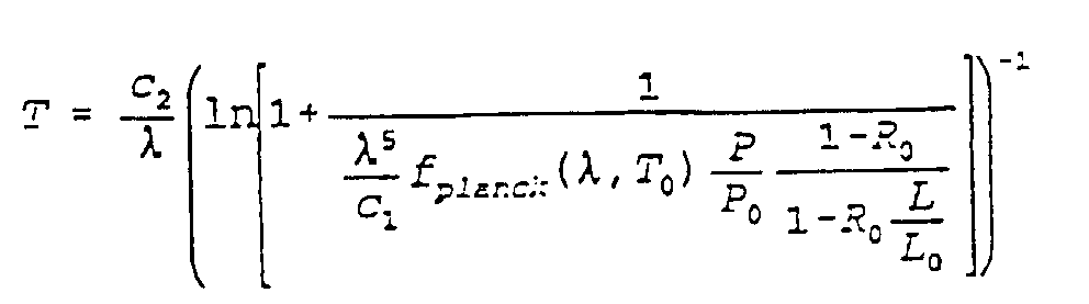 la détermination de l'épaisseur de couche (d) est réalisée par une relation de dépendance prédéfinie (R = f(d)) entre la réflectivité mesurée et l'épaisseur de couche qui est oscillante - en cas d'augmentation de l'épaisseur de couche (d).
 - Procédé selon la revendication 1 ou 2, caractérisé en ce que le rayonnement thermique du substrat (1) et le rayonnement réfléchi d'une source lumineuse (6) sont mesurés respectivement par un détecteur (7, 8) au moyen d'une technique de modulation sensible à la phase appartenant à chaque détecteur, contenant respectivement un hacheur (9, 11) ainsi qu'un amplificateur synchronisé (10 ; 12) qui lui est relié ;en ce que sont mesurés dans une branche détecteur (A) uniquement le rayonnement de la source de lumière (6) réfléchi par le substrat (1) proportionnellement à la réflectivité (R) et dans l'autre détecteur (B) uniquement le rayonnement thermique proportionnellement à ε. f planck ;en ce que les signaux des détecteurs (7, 8) sont traités de manière analogique ou numérique pour déterminer en temps réel la température (T) avec la formule.
- Procédé selon l'une des revendications 1 et 2, caractérisé en ce que la lumière d'une source lumineuse (6) est préparée au moyen d'un hacheur optique (9) dans un premier domaine étroit de fréquences et le rayonnement thermique est modulé par un deuxième hacheur (11) dans un second domaine de fréquences.
- Procédé selon l'une des revendications précédentes, caractérisé en ce que la température (T) déterminée d'après la formule est utilisée pour le réglage du procédé.
- Procédé selon l'une des revendications précédentes, dans lequel la réflectivité (R) est utilisée pour déterminer l'émissivité (ε).
- Procédé selon l'une des revendications précédentes, dans lequel le substrat (1) est opaque.
- Dispositif de mise en oeuvre du procédé selon l'une des revendications précédentes, caractérisé en cequ'un premier détecteur (7) est prévu pour la mesure de l'intensité du rayonnement thermique du substrat dans une branche du rayonnement thermique (B) ;que dans la branche réflectomètre (A) un deuxième détecteur (B) est prévu pour la détermination du rayonnement envoyé par une source de lumière (6) et réfléchi par le substrat (1) ;que la source de lumière (6) de la branche réflectomètre (A) et le rayonnement thermique du substrat (1) sont monochromatisés par le même filtre ou des filtres semblables (3) ;qu'un hacheur (9, 11) ainsi qu'un amplificateur synchrone (10, 12) sont associés respectivement aux détecteurs (7, 8).
- Dispositif selon la revendication 8, caractérisé en ce que l'angle d'incidence de la lumière du réflectomètre et l'angle d'observation de la branche rayonnement thermique avec pyromètre sont égaux.
- Dispositif selon l'une des revendications de dispositif précédentes, caractérisé en ce que la source de lumière (6) est une source de lumière monochromatique, de préférence un laser, une source de lumière blanche sous forme de barres GLOBAR (SIC), un radiateur corps noir ou une lampe halogène.
- Dispositif selon l'une des revendications de dispositif précédentes, caractérisé en ce que les deux branches détecteur (A ; B) sont placées dans un espace séparé de la source de lumière (6) lors d'une incidence non verticale du rayonnement sur le substrat (1).
Applications Claiming Priority (5)
| Application Number | Priority Date | Filing Date | Title |
|---|---|---|---|
| DE4318520 | 1993-06-03 | ||
| DE4318520 | 1993-06-03 | ||
| WOPCT/DE94/00020 | 1994-01-11 | ||
| DE9400020 | 1994-01-11 | ||
| PCT/DE1994/000168 WO1994029681A1 (fr) | 1993-06-03 | 1994-02-16 | Determination simultanee de l'epaisseur des couches et de la temperature du substrat pendant une operation d'enduction |
Publications (2)
| Publication Number | Publication Date |
|---|---|
| EP0701686A1 EP0701686A1 (fr) | 1996-03-20 |
| EP0701686B1 true EP0701686B1 (fr) | 1998-11-18 |
Family
ID=6489594
Family Applications (1)
| Application Number | Title | Priority Date | Filing Date |
|---|---|---|---|
| EP94906879A Expired - Lifetime EP0701686B1 (fr) | 1993-06-03 | 1994-02-16 | Determination simultanee de l'epaisseur des couches et de la temperature du substrat pendant une operation d'enduction |
Country Status (5)
| Country | Link |
|---|---|
| US (1) | US5564830A (fr) |
| EP (1) | EP0701686B1 (fr) |
| AT (1) | ATE173538T1 (fr) |
| CA (1) | CA2164306A1 (fr) |
| DE (1) | DE4419476C2 (fr) |
Cited By (2)
| Publication number | Priority date | Publication date | Assignee | Title |
|---|---|---|---|---|
| CN101055169B (zh) * | 2005-12-16 | 2012-10-10 | 通用电气公司 | 用于无损测定绝缘涂层的方法和装置 |
| EP2887031A1 (fr) | 2013-12-18 | 2015-06-24 | LayTec AG | Procédé d'étalonnage d'un pyromètre à deux longueurs d'ondes, procédé et système pour déterminer la température d'une plaquette semi-conductrice |
Families Citing this family (65)
| Publication number | Priority date | Publication date | Assignee | Title |
|---|---|---|---|---|
| GB9411153D0 (en) * | 1994-06-03 | 1994-07-27 | Land Infrared Ltd | Temperature monitoring |
| US5835225A (en) * | 1994-11-30 | 1998-11-10 | Micron Technology, Inc. | Surface properties detection by reflectance metrology |
| US5757498A (en) * | 1996-05-30 | 1998-05-26 | Klein, Ii; Richard J. | Optical spray coating monitoring system and method |
| US5756369A (en) * | 1996-07-11 | 1998-05-26 | Lsi Logic Corporation | Rapid thermal processing using a narrowband infrared source and feedback |
| US6126744A (en) * | 1996-11-18 | 2000-10-03 | Asm America, Inc. | Method and system for adjusting semiconductor processing equipment |
| US5868840A (en) * | 1996-12-30 | 1999-02-09 | The University Of Northern Iowa Foundation | Paint gun incorporating a laser device |
| US5857625A (en) * | 1996-12-30 | 1999-01-12 | The University Of Northern Iowa Foundation | Paint gun incorporating a laser device |
| US6246098B1 (en) * | 1996-12-31 | 2001-06-12 | Intel Corporation | Apparatus for reducing reflections off the surface of a semiconductor surface |
| WO1998032165A1 (fr) * | 1997-01-21 | 1998-07-23 | Sekidenko Incorporated | Procede de regulation de la temperature d'une couche de semi-conducteurs |
| US6012840A (en) * | 1997-01-27 | 2000-01-11 | The Regents Of The University Of California | Single-fiber multi-color pyrometry |
| US6366861B1 (en) * | 1997-04-25 | 2002-04-02 | Applied Materials, Inc. | Method of determining a wafer characteristic using a film thickness monitor |
| US5841110A (en) * | 1997-08-27 | 1998-11-24 | Steag-Ast Gmbh | Method and apparatus for improved temperature control in rapid thermal processing (RTP) systems |
| JPH1174176A (ja) * | 1997-08-29 | 1999-03-16 | Sony Corp | 半導体装置の製造方法、膜厚最適化装置および膜厚最適化方法 |
| US6022749A (en) | 1998-02-25 | 2000-02-08 | Advanced Micro Devices, Inc. | Using a superlattice to determine the temperature of a semiconductor fabrication process |
| US6535779B1 (en) | 1998-03-06 | 2003-03-18 | Applied Materials, Inc. | Apparatus and method for endpoint control and plasma monitoring |
| US6081334A (en) | 1998-04-17 | 2000-06-27 | Applied Materials, Inc | Endpoint detection for semiconductor processes |
| JP2000082661A (ja) * | 1998-07-02 | 2000-03-21 | Toshiba Corp | 加熱装置,加熱装置の評価法及びパタ―ン形成方法 |
| EP1125314A1 (fr) | 1998-07-10 | 2001-08-22 | Applied Materials, Inc. | Amelioration de la detection de la fin d'operations de fabrication de substrats |
| DE19832833C2 (de) * | 1998-07-21 | 2002-01-31 | Fraunhofer Ges Forschung | Verfahren zur thermographischen Untersuchung eines Werkstückes und Vorrichtung hierfür |
| US6475815B1 (en) * | 1998-12-09 | 2002-11-05 | Matsushita Electric Industrial Co., Ltd. | Method of measuring temperature, method of taking samples for temperature measurement and method for fabricating semiconductor device |
| US6286685B1 (en) | 1999-03-15 | 2001-09-11 | Seh America, Inc. | System and method for wafer thickness sorting |
| US6284986B1 (en) | 1999-03-15 | 2001-09-04 | Seh America, Inc. | Method of determining the thickness of a layer on a silicon substrate |
| WO2000071971A1 (fr) | 1999-05-24 | 2000-11-30 | Luxtron Corporation | Techniques optiques de mesure d'epaisseurs de couche |
| US6570662B1 (en) | 1999-05-24 | 2003-05-27 | Luxtron Corporation | Optical techniques for measuring layer thicknesses and other surface characteristics of objects such as semiconductor wafers |
| DE19928171B4 (de) * | 1999-06-19 | 2011-01-05 | Leybold Optics Gmbh | Verfahren zur kontinuierlichen Bestimmung der optischen Schichtdicke von Beschichtungen |
| US6683695B1 (en) | 1999-07-21 | 2004-01-27 | Electronic Design To Market, Inc. | Method and apparatus for detecting properties of reflective transparent surface coatings on a sheet of transparent material |
| US6328802B1 (en) | 1999-09-14 | 2001-12-11 | Lsi Logic Corporation | Method and apparatus for determining temperature of a semiconductor wafer during fabrication thereof |
| US6449038B1 (en) | 1999-12-13 | 2002-09-10 | Applied Materials, Inc. | Detecting a process endpoint from a change in reflectivity |
| US6682216B1 (en) * | 1999-12-16 | 2004-01-27 | The Regents Of The University Of California | Single-fiber multi-color pyrometry |
| US6824813B1 (en) | 2000-04-06 | 2004-11-30 | Applied Materials Inc | Substrate monitoring method and apparatus |
| US6316277B1 (en) * | 2000-05-30 | 2001-11-13 | Advanced Micro Devices, Inc. | Tuning substrate/resist contrast to maximize defect inspection sensitivity for ultra-thin resist in DUV lithography |
| US6398406B1 (en) | 2000-06-01 | 2002-06-04 | Sandia Corporation | Temperature determination using pyrometry |
| US6352870B1 (en) * | 2000-06-12 | 2002-03-05 | Advanced Micro Devices, Inc. | Method of endpointing plasma strip process by measuring wafer temperature |
| DE10061168C2 (de) * | 2000-11-30 | 2002-12-19 | Laytec Ges Fuer In Situ Und Na | Verfahren zur Messung von Kennwerten eines Schichtsystems während des Schichtaufbaus, insbesondere der Temperatur, insbesondere bei einem Halbleitersystem während der Epitaxie |
| JP3998445B2 (ja) * | 2001-08-31 | 2007-10-24 | 株式会社東芝 | 半導体装置の製造方法、半導体装置の製造装置、半導体装置の製造システム、および半導体製造装置のクリーニング方法 |
| DE10154284A1 (de) * | 2001-11-05 | 2003-05-15 | Rolls Royce Deutschland | Verfahren zum automatischen Auftragen einer Oberflächenschicht |
| US7063747B2 (en) * | 2002-05-29 | 2006-06-20 | Acushnet Company | Coating control system for use on a spherical object |
| US6825933B2 (en) | 2002-06-07 | 2004-11-30 | N&K Technology, Inc. | Computer-implemented reflectance system and method for non-destructive low dose ion implantation monitoring |
| US7009705B1 (en) * | 2002-07-18 | 2006-03-07 | Itt Manufacturing Enterprises, Inc. | Active remote sensing using lock-in amplifiers and beam steering |
| US7341673B2 (en) | 2003-08-12 | 2008-03-11 | Lam Research Corporation | Methods and apparatus for in situ substrate temperature monitoring by electromagnetic radiation emission |
| TWI320951B (en) * | 2002-08-13 | 2010-02-21 | Lam Res Corp | Methods for in situ substrate temperature monitoring by electromagnetic radiation emission |
| DE10258713B4 (de) * | 2002-12-12 | 2010-07-29 | Laytec Gesellschaft Für In-Situ und Nano-Sensorik mbH | Verfahren und Vorrichtung zur Bestimmung charakteristischer Schichtparameter bei hohen Temperaturen |
| US6905624B2 (en) * | 2003-07-07 | 2005-06-14 | Applied Materials, Inc. | Interferometric endpoint detection in a substrate etching process |
| WO2005036601A2 (fr) * | 2003-10-07 | 2005-04-21 | Midwest Research Institute | Caracteristiques de plaquette determinees par reflectometrie, et dispositif et procede pour le traitement de plaquette |
| US20050106876A1 (en) * | 2003-10-09 | 2005-05-19 | Taylor Charles A.Ii | Apparatus and method for real time measurement of substrate temperatures for use in semiconductor growth and wafer processing |
| US8315834B2 (en) * | 2003-12-17 | 2012-11-20 | Siemens Energy, Inc. | System and method for measuring coating thickness |
| JP4216209B2 (ja) * | 2004-03-04 | 2009-01-28 | 大日本スクリーン製造株式会社 | 膜厚測定方法および装置 |
| BE1016003A3 (fr) * | 2004-05-03 | 2006-01-10 | Ct Rech Metallurgiques Asbl | Procede et appareil pour la mesure simultanee de l'epaisseur et de la temperature d'une couche d'oxyde. |
| US7417749B1 (en) | 2004-09-01 | 2008-08-26 | Electric Design To Market, Inc. | Method and apparatus for protecting an optical transmission measurement when sensing transparent materials |
| US20060054843A1 (en) * | 2004-09-13 | 2006-03-16 | Electronic Design To Market, Inc. | Method and apparatus of improving optical reflection images of a laser on a changing surface location |
| DE102005008889B4 (de) * | 2005-02-26 | 2016-07-07 | Leybold Optics Gmbh | Optisches Monitoringsystem für Beschichtungsprozesse |
| US7589843B2 (en) * | 2005-09-27 | 2009-09-15 | Verity Instruments, Inc. | Self referencing heterodyne reflectometer and method for implementing |
| US7652760B1 (en) | 2006-04-05 | 2010-01-26 | Electronic Design To Market, Inc. | System for detecting coatings on transparent or semi-transparent materials |
| US7583368B1 (en) | 2006-04-05 | 2009-09-01 | Electronic Design To Market, Inc. | Method of enhancing measurement of stress in glass |
| WO2007140795A1 (fr) * | 2006-06-02 | 2007-12-13 | Airbus Deutschland Gmbh | Appareil de test et procédé pour détecter une déficience de contact d'une connexion électroconductrice |
| US7549789B2 (en) * | 2007-06-20 | 2009-06-23 | General Electric Company | Method and apparatus for thermographic nondestructive evaluation of an object |
| US7997121B2 (en) * | 2008-07-11 | 2011-08-16 | Savannah River Nuclear Solutions, Llc | Milliwave melter monitoring system |
| US20120244290A1 (en) | 2011-03-24 | 2012-09-27 | United Technologies Corporation | Deposition Substrate Temperature and Monitoring |
| TWI585880B (zh) * | 2011-11-10 | 2017-06-01 | 應用材料股份有限公司 | 透過雷射繞射測量3d半導體結構之溫度的設備及方法 |
| DE102020111293B4 (de) * | 2019-04-24 | 2024-11-07 | Laytec Aktiengesellschaft | Verfahren und Vorrichtung zur in-situ Bestimmung der Temperatur eines Wafers |
| DE102022101809A1 (de) | 2022-01-26 | 2023-07-27 | Aixtron Se | Verfahren zur emissivitätskorrigierten Pyrometrie |
| DE102022101806A1 (de) | 2022-01-26 | 2023-07-27 | Aixtron Se | Verfahren zur emissivitätskorrigierten Pyrometrie |
| DE102023106038A1 (de) | 2023-03-10 | 2024-09-12 | Laytec Aktiengesellschaft | Verfahren zur in-situ Bestimmung der Temperatur eines Wafers |
| DE102023120208B4 (de) | 2023-07-28 | 2025-08-21 | Laytec Aktiengesellschaft | Verfahren und Vorrichtung zur in-situ Bestimmung der Temperatur eines Wafers |
| PL449271A1 (pl) * | 2024-07-18 | 2026-01-19 | Instytut Fizyki Polskiej Akademii Nauk | Sposób kalibracji pirometru optycznego do pomiaru temperatury powierzchni podłoża o nieznanej emisyjności podczas krystalizacji warstw w warunkach wysokiej próżni |
Family Cites Families (22)
| Publication number | Priority date | Publication date | Assignee | Title |
|---|---|---|---|---|
| SU1004755A1 (ru) * | 1980-09-15 | 1983-03-15 | Предприятие П/Я Р-6681 | Оптический способ измерени высоты шероховатости поверхности объекта |
| US4417822A (en) * | 1981-01-28 | 1983-11-29 | Exxon Research And Engineering Company | Laser radiometer |
| JPS58115306A (ja) * | 1981-12-29 | 1983-07-09 | Chugai Ro Kogyo Kaisha Ltd | 塗膜厚連続測定装置 |
| US5231595A (en) * | 1983-06-06 | 1993-07-27 | Minolta Camera Kabushiki Kaisha | Pyrometer |
| US4647774A (en) * | 1985-03-04 | 1987-03-03 | Quantum Logic Corporation | Pyrometer #2 |
| US4647775A (en) * | 1985-03-04 | 1987-03-03 | Quantum Logic Corporation | Pyrometer 1 |
| SU1395939A1 (ru) * | 1986-05-26 | 1988-05-15 | Харьковский авиационный институт им.Н.Е.Жуковского | Способ измерени толщины листового материала |
| JPH01202633A (ja) * | 1988-02-08 | 1989-08-15 | Minolta Camera Co Ltd | 放射温度計 |
| US4919542A (en) * | 1988-04-27 | 1990-04-24 | Ag Processing Technologies, Inc. | Emissivity correction apparatus and method |
| US4956538A (en) * | 1988-09-09 | 1990-09-11 | Texas Instruments, Incorporated | Method and apparatus for real-time wafer temperature measurement using infrared pyrometry in advanced lamp-heated rapid thermal processors |
| US4984902A (en) * | 1989-04-13 | 1991-01-15 | Peak Systems, Inc. | Apparatus and method for compensating for errors in temperature measurement of semiconductor wafers during rapid thermal processing |
| US5029117A (en) * | 1989-04-24 | 1991-07-02 | Tektronix, Inc. | Method and apparatus for active pyrometry |
| US5101111A (en) * | 1989-07-13 | 1992-03-31 | Dainippon Screen Mfg. Co., Ltd. | Method of measuring thickness of film with a reference sample having a known reflectance |
| US5282017A (en) * | 1990-01-05 | 1994-01-25 | Quantum Logic Corporation | Reflectance probe |
| US5166080A (en) * | 1991-04-29 | 1992-11-24 | Luxtron Corporation | Techniques for measuring the thickness of a film formed on a substrate |
| US5239488A (en) * | 1990-04-23 | 1993-08-24 | On-Line Technologies, Inc. | Apparatus and method for determining high temperature surface emissivity through reflectance and radiance measurements |
| JPH07101704B2 (ja) * | 1990-08-09 | 1995-11-01 | アプライド マテリアルズ インコーポレイテッド | ウェーハ上に堆積される薄膜の厚さをその場で測定する方法及び装置 |
| US5156461A (en) * | 1991-05-17 | 1992-10-20 | Texas Instruments Incorporated | Multi-point pyrometry with real-time surface emissivity compensation |
| US5180226A (en) * | 1991-10-30 | 1993-01-19 | Texas Instruments Incorporated | Method and apparatus for precise temperature measurement |
| US5326172A (en) * | 1992-12-14 | 1994-07-05 | The United States Of America As Represented By The Administrator Of The National Aeronautics And Space Administration | Multiwavelength pyrometer for gray and non-gray surfaces in the presence of interfering radiation |
| US5326173A (en) * | 1993-01-11 | 1994-07-05 | Alcan International Limited | Apparatus and method for remote temperature measurement |
| US5308161A (en) * | 1993-02-11 | 1994-05-03 | Quantum Logic Corporation | Pyrometer apparatus for use in rapid thermal processing of semiconductor wafers |
-
1994
- 1994-01-18 US US08/183,176 patent/US5564830A/en not_active Expired - Lifetime
- 1994-02-16 AT AT94906879T patent/ATE173538T1/de not_active IP Right Cessation
- 1994-02-16 EP EP94906879A patent/EP0701686B1/fr not_active Expired - Lifetime
- 1994-02-16 CA CA002164306A patent/CA2164306A1/fr not_active Abandoned
- 1994-06-03 DE DE4419476A patent/DE4419476C2/de not_active Expired - Lifetime
Cited By (2)
| Publication number | Priority date | Publication date | Assignee | Title |
|---|---|---|---|---|
| CN101055169B (zh) * | 2005-12-16 | 2012-10-10 | 通用电气公司 | 用于无损测定绝缘涂层的方法和装置 |
| EP2887031A1 (fr) | 2013-12-18 | 2015-06-24 | LayTec AG | Procédé d'étalonnage d'un pyromètre à deux longueurs d'ondes, procédé et système pour déterminer la température d'une plaquette semi-conductrice |
Also Published As
| Publication number | Publication date |
|---|---|
| DE4419476A1 (de) | 1994-12-15 |
| EP0701686A1 (fr) | 1996-03-20 |
| CA2164306A1 (fr) | 1994-12-22 |
| DE4419476C2 (de) | 1995-10-26 |
| ATE173538T1 (de) | 1998-12-15 |
| US5564830A (en) | 1996-10-15 |
Similar Documents
| Publication | Publication Date | Title |
|---|---|---|
| EP0701686A1 (fr) | Determination simultanee de l'epaisseur des couches et de la temperature du substrat pendant une operation d'enduction | |
| EP0531354B1 (fr) | Procédé de mesure de l'épaisseur et de l'indice de réfraction d'une couche mince sur un substrat et dispositif pour l'exécution de ce procédé | |
| DE69428574T2 (de) | Auf Lichtstreuung basierende Temperaturmessung von Werkstücken in Echtzeit | |
| DE102007042779B4 (de) | Kalibrationssubstrat und -verfahren | |
| DE69314876T2 (de) | Vorrichtung und Verfahren zur Kalibrierung eines Temperatursensors | |
| Hsu et al. | Thermally induced crystallization of amorphous‐titania films | |
| US5568978A (en) | Optical apparatus and method for measuring temperature of a substrate material with a temperature dependent band gap | |
| DE102007034289B3 (de) | Verfahren zur in-situ-Bestimmung der stofflichen Zusammensetzung von optisch dünnen Schichten, Anordnungen zur Durchführung und Anwendungen des Verfahrens | |
| Hodgson | The infra-red properties of some metallic films | |
| DE102014117388B4 (de) | Verfahren zum Kalibrieren einer Pyrometeranordnung eines CVD- oder PVD-Reaktors | |
| EP0033507A2 (fr) | Procédé de production reproductible de couches métalliques | |
| EP1468301A1 (fr) | Procede et dispositif d'essai optique de composants a semi-conducteurs | |
| US6849859B2 (en) | Fabrication of precision optics using an imbedded reference surface | |
| DE102012005428B4 (de) | Vorrichtung zum Bestimmen der Temperatur eines Substrats | |
| DE3834948C2 (de) | Verfahren zum Bestimmen des Brechungsindex der obersten Dünnschicht einer mehrlagigen Schicht | |
| DE3880748T2 (de) | Verfahren und vorrichtung zur messung oder bestimmung einer oder mehrerer eigenschaften oder der identitaet einer probe. | |
| DE2448294A1 (de) | Verfahren und vorrichtung zur bestimmung von schichtdicke und brechungsindex von duennen durchsichtigen schichten | |
| Johnson et al. | Effect of substrate thickness, back surface texture, reflectivity, and thin film interference on optical band-gap thermometry | |
| EP0417791B1 (fr) | Procédé et dispositif pour la compensation de la température du boîtier ou la température ambiante d'un pyromètre | |
| WO1994029681A1 (fr) | Determination simultanee de l'epaisseur des couches et de la temperature du substrat pendant une operation d'enduction | |
| DE69316919T2 (de) | Verfahren und vorrichtung zum messen der temperatur eines objektes, besonders eines halbleiters, mittels ellipsometrie | |
| Ariel et al. | Monitoring HgCdTe layer uniformity by the differential absorption technique | |
| DE102023120208B4 (de) | Verfahren und Vorrichtung zur in-situ Bestimmung der Temperatur eines Wafers | |
| DE102020114734A1 (de) | Verfahren und Vorrichtung zur in-situ Bestimmung der Temperatur einer Probe | |
| DE102015205555A1 (de) | Verfahren und Vorrichtung zur Bestimmung einer Schichteigenschaft sowie Verfahren zum Herstellen einer LED |
Legal Events
| Date | Code | Title | Description |
|---|---|---|---|
| PUAI | Public reference made under article 153(3) epc to a published international application that has entered the european phase |
Free format text: ORIGINAL CODE: 0009012 |
|
| 17P | Request for examination filed |
Effective date: 19951221 |
|
| AK | Designated contracting states |
Kind code of ref document: A1 Designated state(s): AT BE CH DE ES FR GB IE IT LI NL SE |
|
| 17Q | First examination report despatched |
Effective date: 19960902 |
|
| GRAG | Despatch of communication of intention to grant |
Free format text: ORIGINAL CODE: EPIDOS AGRA |
|
| GRAG | Despatch of communication of intention to grant |
Free format text: ORIGINAL CODE: EPIDOS AGRA |
|
| GRAH | Despatch of communication of intention to grant a patent |
Free format text: ORIGINAL CODE: EPIDOS IGRA |
|
| GRAH | Despatch of communication of intention to grant a patent |
Free format text: ORIGINAL CODE: EPIDOS IGRA |
|
| GRAA | (expected) grant |
Free format text: ORIGINAL CODE: 0009210 |
|
| AK | Designated contracting states |
Kind code of ref document: B1 Designated state(s): AT BE CH DE ES FR GB IE IT LI NL SE |
|
| PG25 | Lapsed in a contracting state [announced via postgrant information from national office to epo] |
Ref country code: SE Free format text: THE PATENT HAS BEEN ANNULLED BY A DECISION OF A NATIONAL AUTHORITY Effective date: 19981118 Ref country code: NL Free format text: LAPSE BECAUSE OF FAILURE TO SUBMIT A TRANSLATION OF THE DESCRIPTION OR TO PAY THE FEE WITHIN THE PRESCRIBED TIME-LIMIT Effective date: 19981118 Ref country code: IT Free format text: LAPSE BECAUSE OF FAILURE TO SUBMIT A TRANSLATION OF THE DESCRIPTION OR TO PAY THE FEE WITHIN THE PRE;WARNING: LAPSES OF ITALIAN PATENTS WITH EFFECTIVE DATE BEFORE 2007 MAY HAVE OCCURRED AT ANY TIME BEFORE 2007. THE CORRECT EFFECTIVE DATE MAY BE DIFFERENT FROM THE ONE RECORDED.SCRIBED TIME-LIMIT Effective date: 19981118 Ref country code: GB Free format text: LAPSE BECAUSE OF NON-PAYMENT OF DUE FEES Effective date: 19981118 Ref country code: FR Free format text: LAPSE BECAUSE OF FAILURE TO SUBMIT A TRANSLATION OF THE DESCRIPTION OR TO PAY THE FEE WITHIN THE PRESCRIBED TIME-LIMIT Effective date: 19981118 Ref country code: ES Free format text: THE PATENT HAS BEEN ANNULLED BY A DECISION OF A NATIONAL AUTHORITY Effective date: 19981118 |
|
| REF | Corresponds to: |
Ref document number: 173538 Country of ref document: AT Date of ref document: 19981215 Kind code of ref document: T |
|
| REG | Reference to a national code |
Ref country code: CH Ref legal event code: EP |
|
| REF | Corresponds to: |
Ref document number: 59407307 Country of ref document: DE Date of ref document: 19981224 |
|
| REG | Reference to a national code |
Ref country code: IE Ref legal event code: FG4D Free format text: GERMAN |
|
| PG25 | Lapsed in a contracting state [announced via postgrant information from national office to epo] |
Ref country code: AT Free format text: LAPSE BECAUSE OF NON-PAYMENT OF DUE FEES Effective date: 19990216 |
|
| PG25 | Lapsed in a contracting state [announced via postgrant information from national office to epo] |
Ref country code: LI Free format text: LAPSE BECAUSE OF NON-PAYMENT OF DUE FEES Effective date: 19990228 Ref country code: CH Free format text: LAPSE BECAUSE OF NON-PAYMENT OF DUE FEES Effective date: 19990228 Ref country code: BE Free format text: LAPSE BECAUSE OF NON-PAYMENT OF DUE FEES Effective date: 19990228 |
|
| EN | Fr: translation not filed | ||
| NLV1 | Nl: lapsed or annulled due to failure to fulfill the requirements of art. 29p and 29m of the patents act | ||
| GBV | Gb: ep patent (uk) treated as always having been void in accordance with gb section 77(7)/1977 [no translation filed] |
Effective date: 19981118 |
|
| PG25 | Lapsed in a contracting state [announced via postgrant information from national office to epo] |
Ref country code: IE Free format text: LAPSE BECAUSE OF NON-PAYMENT OF DUE FEES Effective date: 19990820 |
|
| BERE | Be: lapsed |
Owner name: FRAUNHOFER-GESELLSCHAFT ZUR FORDERUNG DER ANGEWAN Effective date: 19990228 |
|
| PLBE | No opposition filed within time limit |
Free format text: ORIGINAL CODE: 0009261 |
|
| STAA | Information on the status of an ep patent application or granted ep patent |
Free format text: STATUS: NO OPPOSITION FILED WITHIN TIME LIMIT |
|
| REG | Reference to a national code |
Ref country code: IE Ref legal event code: FD4D |
|
| REG | Reference to a national code |
Ref country code: CH Ref legal event code: PL |
|
| 26N | No opposition filed | ||
| PGFP | Annual fee paid to national office [announced via postgrant information from national office to epo] |
Ref country code: DE Payment date: 20130220 Year of fee payment: 20 |
|
| REG | Reference to a national code |
Ref country code: DE Ref legal event code: R071 Ref document number: 59407307 Country of ref document: DE |
|
| PG25 | Lapsed in a contracting state [announced via postgrant information from national office to epo] |
Ref country code: DE Free format text: LAPSE BECAUSE OF EXPIRATION OF PROTECTION Effective date: 20140218 |