EP0696089A2 - Steckverbinder - Google Patents
Steckverbinder Download PDFInfo
- Publication number
- EP0696089A2 EP0696089A2 EP95116056A EP95116056A EP0696089A2 EP 0696089 A2 EP0696089 A2 EP 0696089A2 EP 95116056 A EP95116056 A EP 95116056A EP 95116056 A EP95116056 A EP 95116056A EP 0696089 A2 EP0696089 A2 EP 0696089A2
- Authority
- EP
- European Patent Office
- Prior art keywords
- connector
- end portion
- connecting piece
- outer conductor
- forward end
- Prior art date
- Legal status (The legal status is an assumption and is not a legal conclusion. Google has not performed a legal analysis and makes no representation as to the accuracy of the status listed.)
- Granted
Links
- 239000004020 conductor Substances 0.000 claims abstract description 52
- 239000000758 substrate Substances 0.000 description 26
- 238000005476 soldering Methods 0.000 description 10
- 230000013011 mating Effects 0.000 description 9
- 238000010276 construction Methods 0.000 description 7
- 239000011347 resin Substances 0.000 description 4
- 229920005989 resin Polymers 0.000 description 4
- 230000008878 coupling Effects 0.000 description 3
- 238000010168 coupling process Methods 0.000 description 3
- 238000005859 coupling reaction Methods 0.000 description 3
- PNEYBMLMFCGWSK-UHFFFAOYSA-N aluminium oxide Inorganic materials [O-2].[O-2].[O-2].[Al+3].[Al+3] PNEYBMLMFCGWSK-UHFFFAOYSA-N 0.000 description 2
- 239000000463 material Substances 0.000 description 2
- 238000012986 modification Methods 0.000 description 2
- 230000004048 modification Effects 0.000 description 2
- 238000000465 moulding Methods 0.000 description 2
- 239000000919 ceramic Substances 0.000 description 1
- 238000003780 insertion Methods 0.000 description 1
- 230000037431 insertion Effects 0.000 description 1
- 239000011810 insulating material Substances 0.000 description 1
- 229910000679 solder Inorganic materials 0.000 description 1
Images


Classifications
-
- H—ELECTRICITY
- H01—ELECTRIC ELEMENTS
- H01R—ELECTRICALLY-CONDUCTIVE CONNECTIONS; STRUCTURAL ASSOCIATIONS OF A PLURALITY OF MUTUALLY-INSULATED ELECTRICAL CONNECTING ELEMENTS; COUPLING DEVICES; CURRENT COLLECTORS
- H01R24/00—Two-part coupling devices, or either of their cooperating parts, characterised by their overall structure
- H01R24/38—Two-part coupling devices, or either of their cooperating parts, characterised by their overall structure having concentrically or coaxially arranged contacts
- H01R24/40—Two-part coupling devices, or either of their cooperating parts, characterised by their overall structure having concentrically or coaxially arranged contacts specially adapted for high frequency
- H01R24/50—Two-part coupling devices, or either of their cooperating parts, characterised by their overall structure having concentrically or coaxially arranged contacts specially adapted for high frequency mounted on a PCB [Printed Circuit Board]
-
- H—ELECTRICITY
- H01—ELECTRIC ELEMENTS
- H01R—ELECTRICALLY-CONDUCTIVE CONNECTIONS; STRUCTURAL ASSOCIATIONS OF A PLURALITY OF MUTUALLY-INSULATED ELECTRICAL CONNECTING ELEMENTS; COUPLING DEVICES; CURRENT COLLECTORS
- H01R2103/00—Two poles
Definitions
- the present invention generally relates to an electrical connector and more particularly, to a connector of a surface mounting type to be used for connecting various electrical parts or the like onto a circuit board.
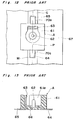
- a connector of a surface mounting type there has been employed, for example, a connector A having a construction as shown in Figs. 12 to 15, and arranged to be coupled with a mating connector B provided with a housing 83, and a socket 82 connected to an inner conductor 81, etc. as illustrated in Fig. 16.
- the connector A includes a case 61 formed with a recess 61a and an inner contact 62 to be fitted into the socket 82 of the connector B and a connector outer conductor 63 provided in said recess 61a, with an inner contact terminal 64 connected with said inner contact 62, and an outer conductor terminal 65 connected with the connector outer conductor 63 being led out from a fixing surface 66 provided at a bottom wall of the case 61 so as to confront a circuit substrate 67 (Figs. 14 and 15).
- a fixing surface 66 provided at a bottom wall of the case 61 so as to confront a circuit substrate 67 (Figs. 14 and 15).
- the connector A by soldering the inner contact terminal 64 and the outer conductor terminal 65, respectively onto a microstrip line M and a grounding pattern G provided on the circuit substrate 67, the connector A is actually mounted on said substrate 67 through electrical and mechanical connection therewith.
- the solder protruding from the soldering surfaces 70 between the connector A and the substrate 67 is indicated at Numeral 70a.
- the connector A is connected and fixed on the circuit substrate 67 at the soldering surfaces 70, since the soldering area is small, and moreover, the connector A is soldered only at two portions, i.e. at the inner contact terminal 64 and the outer conductor terminal 65 (Fig. 12), the fixing surface 66 of the case 61 is raised or floating without contacting the circuit substrate 67 at opposite sides of a line P connecting the inner contact terminal 64 and the outer conductor terminal 65, and therefore, if a prying force in a direction indicated by an arrow X or Y (Fig. 14) is applied during connection with or removal from the mating connector B, there is a possibility that the connector A is undesirably separated from the circuit substrate 67, while a sufficient reliability can not be achieved with respect to the electrical connection thereof.
- an essential object of the present invention is to provide a connector which has a sufficient connecting strength with respect to a substrate, and can be readily fixed onto the substrate in a proper posture without undesirable inclination, etc. during actual mounting.
- Another object of the present invention is to provide a connector of the above described type and a connecting arrangement for the connector, in which height of the connector may be reduced, with sufficiently strong mechanical and electrical connections, while undesirable increase of reflection due to faulty impedance matching is not easily produced.
- a further object of the present invention is to provide a coaxial connector of a chip type, in which characteristic impedance is adapted to be constant over the entire unit through reduction of portions with mismatching.
- a coaxial connector which includes a central conductor and an outer conductor disposed in an insulated state around said central conductor, and a plate-like connecting piece having said central conductor extending upwardly from a forward end portion of said connecting piece.
- the connecting piece has a circular shape at the forward end portion thereof, and a belt-like shape at a base end portion thereof, with part of the circular shape at the forward end portion farthest from the base end portion side being cut off in an arcuate shape.
- the arcuate portion is arranged in its cut off chord length to be equal to a width of the belt-like portion in the vicinity of said circular portion.
- the connecting piece since the part of the circular shape at the forward end portion of the connecting piece is cut off in the arcuate shape, and the arcuate portion is arranged in its cut off chord length to be equal to the width of the belt-like portion in the vicinity of the circular portion, the connecting piece may be equivalently regarded as a belt-like member defined in its width from the forward end to the base portion, with the arcuate protrusions provided at the opposite sides thereof.
- the protrusions may be embedded in resin in the similar manner as in the conventional practice so as to be utilized for fixing of the forward end portion. Therefore, when the protrusions are fixed in the mold resin, even if coupling with or disengagement from the coaxial connector at the jack side is repeatedly effected, matching may be achieved over the entire unit in a state where falling off is prevented.
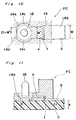
- a plug side connector C to be mounted on a circuit substrate or the like, which includes a case 1 formed therein with a recess 2, an inner contact 3 of a circular columnar shape provided at a central portion of the recess 2, and a partially cylindrical or arcuate connector outer conductor 4 formed by curving a flat plate-like conductor and provided at part of an inner periphery of said recess 2. Adjacent to the upper edge of the connector outer conductor 4, another recess or groove 4a is formed in a circumferential direction thereof. Onto a bottom face 5 of the case 1 forming a fixing surface confronting a substrate D (Fig.
- an inner contact terminal 6 connected with the inner contact 3 and an outer conductor terminal 7 connected with the connector outer conductor 4 are led out. Furthermore, as is most clearly shown in Fig. 4, there are also formed two fixing terminals 14 and 15 on the fixing surface 5 of the case 1.
- the inner contact terminal 6, the outer conductor terminal 7, and the at least two fixing terminals 14 and 15 are respectively disposed so that substantial portions thereof are positioned in regions divided into a first quadrant 16, a second quadrant 17, a third quadrant 18 and a fourth quadrant 19 by lines Q and R, with a central portion of the fixing surface 5 set as an original point.
- the plug connector C is actually mounted on the substrate D.
- the connector C thus mounted are stable, since the inner contact terminal 6, outer conductor terminal 7 and the fixing terminals 14 and 15 are disposed so that the substantial portions thereof are respectively located in all of the four regions defined by the first to fourth quadrants of the fixing surface, and is sufficiently strong even against a prying force applied thereto, thereby providing a positive connection both mechanically and electrically.
- the substantial portion of at least one terminal has only to be disposed in each of the quadrants, and the kinds of the terminals to be disposed in the respective quadrants are not limited, while one terminal may be disposed to bridge the respective quadrants.
- the connector C since the terminals are so disposed that the substantial portion of at least one terminal is located in each of the four regions defined by the first, second, third and fourth quadrants, thereby to connect the respective terminal onto the substrate for fixing, the area at the soldering portion is enlarged for improved bonding strength, while owing to the fact that the fixing terminals are properly positioned, the connector may be mounted on the substrate in a proper attitude, and thus, strong connection which can fully cope with even a stress to pry out the connector, may be achieved.
- Figs. 6 to 8 related to an application of the first embodiment as described so far.
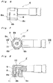
- a jack side connector E as a mating connector to be connected with the plug side connector C described so far.
- the jack side connector E includes a housing 8 as an outer conductor provided with a cylindrical connecting portion 8a for connection with the plug side connector C, and a three-split type center socket 11 as an inner contact connected with an inner conductor 10, and held in an insulated state by an insulating material 9 within the connecting portion 8a.
- the above connecting portion 8a is formed with three slits 8b extending generally in a parallel relation in an axial direction at intervals of 120° so as to provide proper resiliency, while an annular protrusion 8c to be engaged with the groove 4a formed in the connector outer conductor 4 of the plug side connector C referred to earlier is formed, adjacent to the forward edge of said connecting portion 8a.
- the connecting portion 8a of the housing 8 is applied with hardening to provide elasticity required for achieving sufficiently strong connection with the connector outer conductor 4. subsequently, description will be given on the connection between the plug side connector C and the jack side connector E.
- the annular protrusion 8c formed adjacent to the forward edge of the cylindrical connecting portion 8a of the jack side connector E is brought into engagement with the corresponding recess or the groove 4a of the partially cylindrical connector outer conductor 4 of the plug side connector C.
- the protrusion 8c of the connecting portion 8a formed with the slits 8b is thus pressed against the inner wall of the groove 4a by the resiliency thereof for positive connection therebetween.
- the inner contact 3 of the plug connector C is fitted into the three-split center socket 11 of the jack side connector E, and the center socket 11 of the connector E fixedly grasps the inner contact 3 of the connector C for coupling therebetween.
- the present invention may also be applied to connectors and connecting construction thereof in which the inner conductors are of multi-cores.
- the plug side connector makes it possible to achieve positive connection in the case where the outer conductor of the mating connector is of the cylindrical configuration, and moreover, since it is not intended to hold the housing by the resiliency of the connector outer conductor, the connector outer conductor may be reduced in its height for compact size. Furthermore, since the connector outer conductor is not required to have elasticity, it becomes possible to place the connector in a reflow furnace for improved workability.
- the jack side connector has a sufficient resiliency at the connecting portion of the housing, and thus, is improved in the holding force for holding the mating connector.
- the connector connecting construction of the present invention is advantageous in that, since the contact area between the connector outer conductor and the mating connector is increased, concentration of electric current is alleviated for reduction of VSWR (voltage standing wave ratio). Additionally, since sufficiently strong mechanical and electrical connection can be achieved, even when a prying force is applied to the mating connector, there is no possibility that electrical discontinuity takes place due to breakage of the electrical connection, etc.
- the jack side coaxial connector FE has the construction generally similar to that of the connector E of Figs. 6,7 and 8, and includes a housing 8' having an outer conductor 8a' formed with split grooves 8b' and a socket-like central conductor 11', with a coaxial cable CB being connected thereto as shown.
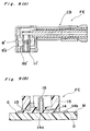
- the plug side coaxial connector FC as shown in Fig. 9(B) includes a central conductor 16 and an outer conductor 13 disposed in an insulated state around the central conductor 16 so as to partially surround said central conductor 16, and a plate-like connecting piece 14 provided in a manner as describe hereinbelow.
- the connecting piece 14 has a forward end portion 14a in a circular shape provided with the central conductor 16 extending upwardly therefrom and a base end portion 14b connected thereto.
- the central conductor 16 is formed to extend upwardly from the forward end portion 14a of the connecting piece 14, with part of the base end portion 14b and the outer conductor 13, and the central conductor 16 being exposed form a molding resin 15 as shown in Fig. 9(B). Fixing of such a coaxial plug side connector FC onto the circuit board D is effected by soldering the under surface of the outer conductor 13 and the base end portion 14b of the connecting piece 14, respectively onto the grounding pattern G and the strip line M formed on the circuit board D.
- the base end portion 14b is formed with a small width portion a at its side leading to the forward end portion 14a, and a large width portion b at the side opposite thereto, with a stepped or folded portion f being formed at the portion between said small width portion a and large width portion b so that said small width portion a is higher than said large width portion b (Fig. 11).
- chord length l at the cut off portion 14d, the width W of the large width portion b, the width W' of the small width portion a are so defined in dimensions as to achieve matching over the entire connecting piece 14, and the dimensions for the widths W and W' are determined based on the height between the undersurface of the substrate D and the large width portion b or the small width portion a and dielectric constants therebetween, with the cut off chord length l being set to be equal to the width W' of the small width portion a. subsequently, calculations with respect to the dimensions for the widths W and W' and the chord length l will be explained.
- the widths W and W' will be calculated.
- the width w is calculated, when a characteristic impedance Zo to be matched is determined, based on such impedance Zo, a height h from the undersurface of the circuit substrate D up to the large width portion b, and dielectric constant ⁇ r for the portion with the height h, i.e. the substrate D, and equations (1) and (3) given below, while through employment of equations (2) and (3) instead of the equations (1) and (3), two sets of values are to be computed.
- the other width value W' is calculated in the similar manner by setting a height h' from the undersurface of the substrate D up to the small width portion a as the height h, and also, by using as the dielectric constant ⁇ r, a dielectric constant ⁇ r' in which the nature of a molding resin 15 present therebetween and made of a material different from that of the wiring substrate D of ceramics, alumina, etc. is taken into consideration, and then, the value l is set to be equal to the value W' thus obtained.
- the connecting piece 14 is prepared so as to satisfy the dimensions W,W' and l thus obtained, the portion ranging from the narrow portion a of the base end portion 14b to the forward end portion 14a may be regarded equivalently as the belt-like portion with a predetermined width defined by W' having protrusions 14c at opposite sides thereof (Fig. 10).
- the width of the base end portion 14b of the connecting piece 14 is varied on the way, the present invention is not limited in its application to such an arrangement alone, but may be similarly applied, for example, to a case where the base end portion 14b is set to be constant in width over its entire length, or where its width is altered in more than three levels at more than two places on the way.
- the connecting piece since the forward end portion of the connecting piece is formed into a circular shape cut in an arcuate shape at its one portion, with the cut off chord length at said cut off portion being made equal to the with of the portion connected with the forward end of the base end portion, the connecting piece may be regarded equivalently as an belt-like member restricted in its width and having the arcuate protrusions at its opposite sides, and when the protrusions are fixed in the mold, even if coupling or disengagement with respect to the jack side coaxial connector is repeatedly effected, matching may be achieved on the whole in the state where falling off of said connector is advantageously prevented. Accordingly, for example, in the case where the connector of the present invention is mounted on a wiring substrate made of alumina, VSWR (voltage standing wave ratio) may be limited below 1.2 at 1.09 during 2GHz.
Landscapes
- Coupling Device And Connection With Printed Circuit (AREA)
Applications Claiming Priority (10)
| Application Number | Priority Date | Filing Date | Title |
|---|---|---|---|
| JP112618/89U | 1989-09-25 | ||
| JP11261889U | 1989-09-25 | ||
| JP112619/89U | 1989-09-25 | ||
| JP11261889U JPH0350780U (de) | 1989-09-25 | 1989-09-25 | |
| JP1989112619U JPH0743976Y2 (ja) | 1989-09-25 | 1989-09-25 | コネクタの接続構造 |
| JP11261989U | 1989-09-25 | ||
| JP124649/89U | 1989-10-25 | ||
| JP12464989U | 1989-10-25 | ||
| JP1989124649U JPH0724791Y2 (ja) | 1989-10-25 | 1989-10-25 | 同軸コネクタ |
| EP90117495A EP0419938B1 (de) | 1989-09-25 | 1990-09-11 | Steckverbinder |
Related Parent Applications (2)
| Application Number | Title | Priority Date | Filing Date |
|---|---|---|---|
| EP90117495.3 Division | 1990-09-11 | ||
| EP90117495A Division EP0419938B1 (de) | 1989-09-25 | 1990-09-11 | Steckverbinder |
Publications (3)
| Publication Number | Publication Date |
|---|---|
| EP0696089A2 true EP0696089A2 (de) | 1996-02-07 |
| EP0696089A3 EP0696089A3 (de) | 1996-10-30 |
| EP0696089B1 EP0696089B1 (de) | 2002-04-10 |
Family
ID=27312294
Family Applications (2)
| Application Number | Title | Priority Date | Filing Date |
|---|---|---|---|
| EP90117495A Expired - Lifetime EP0419938B1 (de) | 1989-09-25 | 1990-09-11 | Steckverbinder |
| EP95116056A Expired - Lifetime EP0696089B1 (de) | 1989-09-25 | 1990-09-11 | Steckverbinder |
Family Applications Before (1)
| Application Number | Title | Priority Date | Filing Date |
|---|---|---|---|
| EP90117495A Expired - Lifetime EP0419938B1 (de) | 1989-09-25 | 1990-09-11 | Steckverbinder |
Country Status (3)
| Country | Link |
|---|---|
| US (1) | US5078621A (de) |
| EP (2) | EP0419938B1 (de) |
| DE (2) | DE69029241T2 (de) |
Cited By (1)
| Publication number | Priority date | Publication date | Assignee | Title |
|---|---|---|---|---|
| TWI648929B (zh) * | 2016-10-14 | 2019-01-21 | 日商日本壓著端子製造股份有限公司 | 同軸連接器之安裝構造 |
Families Citing this family (30)
| Publication number | Priority date | Publication date | Assignee | Title |
|---|---|---|---|---|
| US6026311A (en) * | 1993-05-28 | 2000-02-15 | Superconductor Technologies, Inc. | High temperature superconducting structures and methods for high Q, reduced intermodulation resonators and filters |
| US7231238B2 (en) | 1989-01-13 | 2007-06-12 | Superconductor Technologies, Inc. | High temperature spiral snake superconducting resonator having wider runs with higher current density |
| FR2677816B1 (fr) | 1991-06-17 | 1995-04-28 | Radiall Sa | Connecteur coaxial pour le raccordement d'un cable coaxial a une carte imprimee de circuit electronique. |
| EP0545289B1 (de) * | 1991-11-30 | 1997-03-05 | Murata Manufacturing Co., Ltd. | Koaxialleiter/Mikrostreifenleitungsübergang |
| JPH07135053A (ja) * | 1993-11-08 | 1995-05-23 | Murata Mfg Co Ltd | 同軸コネクタ及び同軸コネクタの実装構造 |
| JP3246141B2 (ja) * | 1993-11-18 | 2002-01-15 | 株式会社村田製作所 | 誘電体共振器装置 |
| JP3298279B2 (ja) * | 1993-12-24 | 2002-07-02 | 株式会社村田製作所 | 誘電体共振器装置、その結合係数調整方法及びその製造装置 |
| DE69428509T2 (de) * | 1993-12-28 | 2002-05-16 | Murata Mfg. Co., Ltd. | TM-Zweifachmodusresonator und -filter |
| US6074217A (en) * | 1995-05-25 | 2000-06-13 | Murata Manufacturing Co., Ltd. | Coaxial connector receptacle |
| US5597323A (en) * | 1995-08-07 | 1997-01-28 | The Whitaker Corporation | RF connector jack and plug assembly |
| DE19536276A1 (de) * | 1995-09-28 | 1997-04-03 | Siemens Ag | Einrichtung zum Anschluß eines Koaxialverbinders an einer Leiterplatte in SM-Technik |
| US5718592A (en) * | 1995-11-16 | 1998-02-17 | The Whitaker Corporation | Surface mountable electrical connector assembley |
| USD400170S (en) | 1996-06-13 | 1998-10-27 | Smk Corporation | Coaxial connector |
| JP3269436B2 (ja) * | 1997-09-19 | 2002-03-25 | 株式会社村田製作所 | インサート樹脂成形品の製造方法 |
| AU2783000A (en) † | 1999-05-18 | 2000-12-05 | Keith Louis Eichmann | A plug for connection to an rca or phono type socket |
| US6224421B1 (en) | 2000-02-29 | 2001-05-01 | Palco Connector, Inc. | Multi-part connector |
| FR2818448B1 (fr) * | 2000-12-18 | 2006-02-03 | Sagem | Connecteur de puissance pour carte a circuit imprime |
| USD457496S1 (en) | 2001-07-16 | 2002-05-21 | Hon Hai Precision Ind. Co., Ltd. | Cable end connector |
| JP2003163517A (ja) | 2001-11-28 | 2003-06-06 | Alps Electric Co Ltd | 誘電体共振装置 |
| US6533610B1 (en) * | 2001-12-24 | 2003-03-18 | Hon Hai Precision Ind. Co., Ltd. | Low-profile RF connector assembly |
| US20030222732A1 (en) * | 2002-05-29 | 2003-12-04 | Superconductor Technologies, Inc. | Narrow-band filters with zig-zag hairpin resonator |
| US6700459B2 (en) * | 2002-05-29 | 2004-03-02 | Superconductor Technologies, Inc. | Dual-mode bandpass filter with direct capacitive couplings and far-field suppression structures |
| JP3090812U (ja) * | 2002-06-18 | 2002-12-26 | アルプス電気株式会社 | 高周波モジュール |
| JP3761501B2 (ja) * | 2002-07-31 | 2006-03-29 | 本多通信工業株式会社 | 同軸コネクタ及びそれが実装されるグランドパッド |
| JP3834309B2 (ja) * | 2002-12-26 | 2006-10-18 | ヒロセ電機株式会社 | 同軸電気コネクタ |
| JP2005251746A (ja) | 2004-03-02 | 2005-09-15 | Tyco Electronics Amp Gmbh | 超小型プラグ・ソケットコネクタ |
| TWI401851B (zh) * | 2008-01-30 | 2013-07-11 | Harumoto Prec Co Ltd | Cable connector assembly method |
| JP5051796B2 (ja) * | 2010-04-20 | 2012-10-17 | 日本航空電子工業株式会社 | コネクタ |
| CN202111264U (zh) * | 2011-03-25 | 2012-01-11 | 富士康(昆山)电脑接插件有限公司 | 射频连接器 |
| JP6588403B2 (ja) * | 2016-08-09 | 2019-10-09 | ヒロセ電機株式会社 | 同軸コネクタ |
Family Cites Families (9)
| Publication number | Priority date | Publication date | Assignee | Title |
|---|---|---|---|---|
| GB1111347A (en) * | 1966-03-15 | 1968-04-24 | Dereham Engineering Ltd | Improved co-axial plug and socket coupling |
| US3601776A (en) * | 1969-05-20 | 1971-08-24 | Symbolic Displays Inc | Electrical connectors |
| US4453796A (en) * | 1982-06-21 | 1984-06-12 | Amp Incorporated | Coaxial connector plug |
| US4603926A (en) * | 1983-12-29 | 1986-08-05 | Rca Corporation | Connector for joining microstrip transmission lines |
| US4795991A (en) * | 1986-01-13 | 1989-01-03 | Murata Manufacturing Co., Ltd. | Inlet type noise filter directly mounted to a PC board |
| JPS62285378A (ja) * | 1986-06-04 | 1987-12-11 | ヒロセ電機株式会社 | 雌形同軸コネクタとその製造方法 |
| US4795352A (en) * | 1988-02-01 | 1989-01-03 | Amp Incorporated | Microcoaxial connector family |
| US4846711A (en) * | 1988-08-09 | 1989-07-11 | Amp Incorporated | Coaxial connector in a housing block |
| EP0370833B1 (de) * | 1988-11-25 | 1995-04-19 | Molex Incorporated | Kreisförmiger Miniatur-Din-Verbinder |
-
1990
- 1990-09-11 DE DE69029241T patent/DE69029241T2/de not_active Expired - Lifetime
- 1990-09-11 EP EP90117495A patent/EP0419938B1/de not_active Expired - Lifetime
- 1990-09-11 DE DE69033945T patent/DE69033945T2/de not_active Expired - Lifetime
- 1990-09-11 EP EP95116056A patent/EP0696089B1/de not_active Expired - Lifetime
- 1990-09-14 US US07/582,614 patent/US5078621A/en not_active Expired - Lifetime
Non-Patent Citations (1)
| Title |
|---|
| None |
Cited By (1)
| Publication number | Priority date | Publication date | Assignee | Title |
|---|---|---|---|---|
| TWI648929B (zh) * | 2016-10-14 | 2019-01-21 | 日商日本壓著端子製造股份有限公司 | 同軸連接器之安裝構造 |
Also Published As
| Publication number | Publication date |
|---|---|
| DE69029241T2 (de) | 1997-04-30 |
| DE69033945D1 (de) | 2002-05-16 |
| EP0419938A2 (de) | 1991-04-03 |
| EP0419938B1 (de) | 1996-11-27 |
| EP0419938A3 (en) | 1993-02-03 |
| DE69033945T2 (de) | 2002-10-10 |
| US5078621A (en) | 1992-01-07 |
| DE69029241D1 (de) | 1997-01-09 |
| EP0696089B1 (de) | 2002-04-10 |
| EP0696089A3 (de) | 1996-10-30 |
Similar Documents
| Publication | Publication Date | Title |
|---|---|---|
| EP0419938B1 (de) | Steckverbinder | |
| KR950007430B1 (ko) | 저 프로파일 전기 접속기 | |
| US4487464A (en) | Electrical socket connector construction | |
| US5498167A (en) | Board to board electrical connectors | |
| EP0567007B1 (de) | Elektrischer Verbinder zur Oberflächenmontage | |
| EP0146242B1 (de) | Elektrischer Verbinder für einen Chipträger | |
| US6607400B1 (en) | Low profile RF connector assembly | |
| US5558540A (en) | Multi-connector assembly | |
| US5580280A (en) | Filtered electrical connector | |
| US4143342A (en) | Micro-circuit arrangements | |
| JPH0418436B2 (de) | ||
| US6478586B1 (en) | Electrical connector having conductive terminals that are provided with a dielectric coating | |
| EP0454977A1 (de) | Elektrischer Steckverbinder mit in eine Isolatorplatte eingebetteten Kontaktstreifen für Leiterplatten | |
| US5964594A (en) | Electrical connector | |
| EP0109297B1 (de) | Elektrische Kontaktorgane und Zusammenbau elektrischer Verbinder | |
| CA2025095C (en) | Coaxial pin connector having an array of conductive hollow cylindrical structures | |
| EP0928047B1 (de) | Elektrischer Steckverbinder für Halbleiterbauelemente | |
| US4842527A (en) | Contact assembly for interconnecting circuit board and a coaxial connector | |
| US6338633B1 (en) | Electrical connector with improved contacts | |
| US6109932A (en) | Three-dimensional electrical interconnection system | |
| JP3824352B2 (ja) | 電気コネクタ | |
| TWI907207B (zh) | 懸浮連接器及其組裝方式 | |
| JPS6353869A (ja) | サ−フェスマウントコネクタ | |
| KR102679519B1 (ko) | 리셉터클 커넥터 | |
| WO1995032605A1 (en) | Printed circuit board socket |
Legal Events
| Date | Code | Title | Description |
|---|---|---|---|
| PUAI | Public reference made under article 153(3) epc to a published international application that has entered the european phase |
Free format text: ORIGINAL CODE: 0009012 |
|
| 17P | Request for examination filed |
Effective date: 19951012 |
|
| AC | Divisional application: reference to earlier application |
Ref document number: 419938 Country of ref document: EP |
|
| AK | Designated contracting states |
Kind code of ref document: A2 Designated state(s): DE GB SE |
|
| PUAL | Search report despatched |
Free format text: ORIGINAL CODE: 0009013 |
|
| AK | Designated contracting states |
Kind code of ref document: A3 Designated state(s): DE GB SE |
|
| 17Q | First examination report despatched |
Effective date: 19980826 |
|
| GRAG | Despatch of communication of intention to grant |
Free format text: ORIGINAL CODE: EPIDOS AGRA |
|
| GRAG | Despatch of communication of intention to grant |
Free format text: ORIGINAL CODE: EPIDOS AGRA |
|
| GRAH | Despatch of communication of intention to grant a patent |
Free format text: ORIGINAL CODE: EPIDOS IGRA |
|
| GRAH | Despatch of communication of intention to grant a patent |
Free format text: ORIGINAL CODE: EPIDOS IGRA |
|
| REG | Reference to a national code |
Ref country code: GB Ref legal event code: IF02 |
|
| GRAA | (expected) grant |
Free format text: ORIGINAL CODE: 0009210 |
|
| AC | Divisional application: reference to earlier application |
Ref document number: 419938 Country of ref document: EP |
|
| AK | Designated contracting states |
Kind code of ref document: B1 Designated state(s): DE GB SE |
|
| RIC1 | Information provided on ipc code assigned before grant |
Free format text: 7H 01R 13/646 A |
|
| REF | Corresponds to: |
Ref document number: 69033945 Country of ref document: DE Date of ref document: 20020516 |
|
| PLBE | No opposition filed within time limit |
Free format text: ORIGINAL CODE: 0009261 |
|
| STAA | Information on the status of an ep patent application or granted ep patent |
Free format text: STATUS: NO OPPOSITION FILED WITHIN TIME LIMIT |
|
| 26N | No opposition filed |
Effective date: 20030113 |
|
| PGFP | Annual fee paid to national office [announced via postgrant information from national office to epo] |
Ref country code: SE Payment date: 20090910 Year of fee payment: 20 Ref country code: GB Payment date: 20090909 Year of fee payment: 20 |
|
| PGFP | Annual fee paid to national office [announced via postgrant information from national office to epo] |
Ref country code: DE Payment date: 20090903 Year of fee payment: 20 |
|
| REG | Reference to a national code |
Ref country code: GB Ref legal event code: PE20 Expiry date: 20100910 |
|
| EUG | Se: european patent has lapsed | ||
| PG25 | Lapsed in a contracting state [announced via postgrant information from national office to epo] |
Ref country code: GB Free format text: LAPSE BECAUSE OF EXPIRATION OF PROTECTION Effective date: 20100910 |
|
| PG25 | Lapsed in a contracting state [announced via postgrant information from national office to epo] |
Ref country code: DE Free format text: LAPSE BECAUSE OF EXPIRATION OF PROTECTION Effective date: 20100911 |