EP0695006B1 - Méthode de production d'un composé laser à semi-conducteur - Google Patents
Méthode de production d'un composé laser à semi-conducteur Download PDFInfo
- Publication number
- EP0695006B1 EP0695006B1 EP95115775A EP95115775A EP0695006B1 EP 0695006 B1 EP0695006 B1 EP 0695006B1 EP 95115775 A EP95115775 A EP 95115775A EP 95115775 A EP95115775 A EP 95115775A EP 0695006 B1 EP0695006 B1 EP 0695006B1
- Authority
- EP
- European Patent Office
- Prior art keywords
- layer
- etching stop
- gaas
- gainp
- stop layer
- Prior art date
- Legal status (The legal status is an assumption and is not a legal conclusion. Google has not performed a legal analysis and makes no representation as to the accuracy of the status listed.)
- Expired - Lifetime
Links
- 239000004065 semiconductor Substances 0.000 title claims description 85
- 238000004519 manufacturing process Methods 0.000 title description 19
- 150000001875 compounds Chemical class 0.000 title description 9
- 229910001218 Gallium arsenide Inorganic materials 0.000 claims description 120
- 238000005530 etching Methods 0.000 claims description 93
- 239000000758 substrate Substances 0.000 claims description 89
- 230000003287 optical effect Effects 0.000 claims description 55
- 238000010521 absorption reaction Methods 0.000 claims description 52
- 239000013078 crystal Substances 0.000 claims description 44
- 238000000034 method Methods 0.000 claims description 37
- 229910000980 Aluminium gallium arsenide Inorganic materials 0.000 claims description 33
- 125000005842 heteroatom Chemical group 0.000 claims description 31
- 229910052738 indium Inorganic materials 0.000 claims description 27
- 230000008859 change Effects 0.000 claims description 4
- 238000010438 heat treatment Methods 0.000 claims description 2
- 230000001678 irradiating effect Effects 0.000 claims description 2
- 238000001451 molecular beam epitaxy Methods 0.000 description 45
- 229910052698 phosphorus Inorganic materials 0.000 description 26
- 238000001704 evaporation Methods 0.000 description 17
- 230000008020 evaporation Effects 0.000 description 16
- 230000010355 oscillation Effects 0.000 description 13
- 239000012535 impurity Substances 0.000 description 9
- 230000005855 radiation Effects 0.000 description 9
- 230000000052 comparative effect Effects 0.000 description 8
- 230000006866 deterioration Effects 0.000 description 7
- QVGXLLKOCUKJST-UHFFFAOYSA-N atomic oxygen Chemical compound [O] QVGXLLKOCUKJST-UHFFFAOYSA-N 0.000 description 6
- 230000015572 biosynthetic process Effects 0.000 description 6
- 229910052760 oxygen Inorganic materials 0.000 description 6
- 239000001301 oxygen Substances 0.000 description 6
- 229910052581 Si3N4 Inorganic materials 0.000 description 5
- 229910052733 gallium Inorganic materials 0.000 description 5
- HQVNEWCFYHHQES-UHFFFAOYSA-N silicon nitride Chemical compound N12[Si]34N5[Si]62N3[Si]51N64 HQVNEWCFYHHQES-UHFFFAOYSA-N 0.000 description 5
- 238000009413 insulation Methods 0.000 description 4
- 238000011109 contamination Methods 0.000 description 3
- 239000000203 mixture Substances 0.000 description 3
- 229910000530 Gallium indium arsenide Inorganic materials 0.000 description 2
- VYPSYNLAJGMNEJ-UHFFFAOYSA-N Silicium dioxide Chemical compound O=[Si]=O VYPSYNLAJGMNEJ-UHFFFAOYSA-N 0.000 description 2
- 229910052782 aluminium Inorganic materials 0.000 description 2
- 229910052785 arsenic Inorganic materials 0.000 description 2
- 230000008901 benefit Effects 0.000 description 2
- 238000005229 chemical vapour deposition Methods 0.000 description 2
- 230000000694 effects Effects 0.000 description 2
- 239000000463 material Substances 0.000 description 2
- 229910052814 silicon oxide Inorganic materials 0.000 description 2
- 230000003466 anti-cipated effect Effects 0.000 description 1
- 238000009792 diffusion process Methods 0.000 description 1
- 230000010365 information processing Effects 0.000 description 1
- 238000004020 luminiscence type Methods 0.000 description 1
- 239000002184 metal Substances 0.000 description 1
- 229910052751 metal Inorganic materials 0.000 description 1
- 238000012986 modification Methods 0.000 description 1
- 230000004048 modification Effects 0.000 description 1
- 238000001259 photo etching Methods 0.000 description 1
- 238000005424 photoluminescence Methods 0.000 description 1
- 230000008569 process Effects 0.000 description 1
- 230000009467 reduction Effects 0.000 description 1
- 230000035945 sensitivity Effects 0.000 description 1
- 238000009751 slip forming Methods 0.000 description 1
Images


Classifications
-
- H—ELECTRICITY
- H01—ELECTRIC ELEMENTS
- H01S—DEVICES USING THE PROCESS OF LIGHT AMPLIFICATION BY STIMULATED EMISSION OF RADIATION [LASER] TO AMPLIFY OR GENERATE LIGHT; DEVICES USING STIMULATED EMISSION OF ELECTROMAGNETIC RADIATION IN WAVE RANGES OTHER THAN OPTICAL
- H01S5/00—Semiconductor lasers
- H01S5/30—Structure or shape of the active region; Materials used for the active region
- H01S5/32—Structure or shape of the active region; Materials used for the active region comprising PN junctions, e.g. hetero- or double- heterostructures
- H01S5/323—Structure or shape of the active region; Materials used for the active region comprising PN junctions, e.g. hetero- or double- heterostructures in AIIIBV compounds, e.g. AlGaAs-laser, InP-based laser
- H01S5/32308—Structure or shape of the active region; Materials used for the active region comprising PN junctions, e.g. hetero- or double- heterostructures in AIIIBV compounds, e.g. AlGaAs-laser, InP-based laser emitting light at a wavelength less than 900 nm
- H01S5/32325—Structure or shape of the active region; Materials used for the active region comprising PN junctions, e.g. hetero- or double- heterostructures in AIIIBV compounds, e.g. AlGaAs-laser, InP-based laser emitting light at a wavelength less than 900 nm red laser based on InGaP
-
- H—ELECTRICITY
- H01—ELECTRIC ELEMENTS
- H01L—SEMICONDUCTOR DEVICES NOT COVERED BY CLASS H10
- H01L21/00—Processes or apparatus adapted for the manufacture or treatment of semiconductor or solid state devices or of parts thereof
- H01L21/02—Manufacture or treatment of semiconductor devices or of parts thereof
- H01L21/02104—Forming layers
- H01L21/02365—Forming inorganic semiconducting materials on a substrate
- H01L21/02367—Substrates
- H01L21/0237—Materials
- H01L21/02387—Group 13/15 materials
- H01L21/02395—Arsenides
-
- H—ELECTRICITY
- H01—ELECTRIC ELEMENTS
- H01L—SEMICONDUCTOR DEVICES NOT COVERED BY CLASS H10
- H01L21/00—Processes or apparatus adapted for the manufacture or treatment of semiconductor or solid state devices or of parts thereof
- H01L21/02—Manufacture or treatment of semiconductor devices or of parts thereof
- H01L21/02104—Forming layers
- H01L21/02365—Forming inorganic semiconducting materials on a substrate
- H01L21/02436—Intermediate layers between substrates and deposited layers
- H01L21/02439—Materials
- H01L21/02455—Group 13/15 materials
- H01L21/02461—Phosphides
-
- H—ELECTRICITY
- H01—ELECTRIC ELEMENTS
- H01L—SEMICONDUCTOR DEVICES NOT COVERED BY CLASS H10
- H01L21/00—Processes or apparatus adapted for the manufacture or treatment of semiconductor or solid state devices or of parts thereof
- H01L21/02—Manufacture or treatment of semiconductor devices or of parts thereof
- H01L21/02104—Forming layers
- H01L21/02365—Forming inorganic semiconducting materials on a substrate
- H01L21/02436—Intermediate layers between substrates and deposited layers
- H01L21/02439—Materials
- H01L21/02455—Group 13/15 materials
- H01L21/02463—Arsenides
-
- H—ELECTRICITY
- H01—ELECTRIC ELEMENTS
- H01L—SEMICONDUCTOR DEVICES NOT COVERED BY CLASS H10
- H01L21/00—Processes or apparatus adapted for the manufacture or treatment of semiconductor or solid state devices or of parts thereof
- H01L21/02—Manufacture or treatment of semiconductor devices or of parts thereof
- H01L21/02104—Forming layers
- H01L21/02365—Forming inorganic semiconducting materials on a substrate
- H01L21/02436—Intermediate layers between substrates and deposited layers
- H01L21/02494—Structure
- H01L21/02496—Layer structure
- H01L21/02505—Layer structure consisting of more than two layers
-
- H—ELECTRICITY
- H01—ELECTRIC ELEMENTS
- H01L—SEMICONDUCTOR DEVICES NOT COVERED BY CLASS H10
- H01L21/00—Processes or apparatus adapted for the manufacture or treatment of semiconductor or solid state devices or of parts thereof
- H01L21/02—Manufacture or treatment of semiconductor devices or of parts thereof
- H01L21/02104—Forming layers
- H01L21/02365—Forming inorganic semiconducting materials on a substrate
- H01L21/02518—Deposited layers
- H01L21/02521—Materials
- H01L21/02538—Group 13/15 materials
- H01L21/02546—Arsenides
-
- H—ELECTRICITY
- H01—ELECTRIC ELEMENTS
- H01L—SEMICONDUCTOR DEVICES NOT COVERED BY CLASS H10
- H01L21/00—Processes or apparatus adapted for the manufacture or treatment of semiconductor or solid state devices or of parts thereof
- H01L21/02—Manufacture or treatment of semiconductor devices or of parts thereof
- H01L21/02104—Forming layers
- H01L21/02365—Forming inorganic semiconducting materials on a substrate
- H01L21/02612—Formation types
- H01L21/02617—Deposition types
- H01L21/02631—Physical deposition at reduced pressure, e.g. MBE, sputtering, evaporation
-
- H—ELECTRICITY
- H01—ELECTRIC ELEMENTS
- H01L—SEMICONDUCTOR DEVICES NOT COVERED BY CLASS H10
- H01L21/00—Processes or apparatus adapted for the manufacture or treatment of semiconductor or solid state devices or of parts thereof
- H01L21/02—Manufacture or treatment of semiconductor devices or of parts thereof
- H01L21/02104—Forming layers
- H01L21/02365—Forming inorganic semiconducting materials on a substrate
- H01L21/02656—Special treatments
- H01L21/02658—Pretreatments
-
- H—ELECTRICITY
- H01—ELECTRIC ELEMENTS
- H01L—SEMICONDUCTOR DEVICES NOT COVERED BY CLASS H10
- H01L31/00—Semiconductor devices sensitive to infrared radiation, light, electromagnetic radiation of shorter wavelength or corpuscular radiation and specially adapted either for the conversion of the energy of such radiation into electrical energy or for the control of electrical energy by such radiation; Processes or apparatus specially adapted for the manufacture or treatment thereof or of parts thereof; Details thereof
- H01L31/08—Semiconductor devices sensitive to infrared radiation, light, electromagnetic radiation of shorter wavelength or corpuscular radiation and specially adapted either for the conversion of the energy of such radiation into electrical energy or for the control of electrical energy by such radiation; Processes or apparatus specially adapted for the manufacture or treatment thereof or of parts thereof; Details thereof in which radiation controls flow of current through the device, e.g. photoresistors
- H01L31/10—Semiconductor devices sensitive to infrared radiation, light, electromagnetic radiation of shorter wavelength or corpuscular radiation and specially adapted either for the conversion of the energy of such radiation into electrical energy or for the control of electrical energy by such radiation; Processes or apparatus specially adapted for the manufacture or treatment thereof or of parts thereof; Details thereof in which radiation controls flow of current through the device, e.g. photoresistors characterised by potential barriers, e.g. phototransistors
- H01L31/101—Devices sensitive to infrared, visible or ultraviolet radiation
- H01L31/102—Devices sensitive to infrared, visible or ultraviolet radiation characterised by only one potential barrier
- H01L31/105—Devices sensitive to infrared, visible or ultraviolet radiation characterised by only one potential barrier the potential barrier being of the PIN type
-
- H—ELECTRICITY
- H01—ELECTRIC ELEMENTS
- H01L—SEMICONDUCTOR DEVICES NOT COVERED BY CLASS H10
- H01L31/00—Semiconductor devices sensitive to infrared radiation, light, electromagnetic radiation of shorter wavelength or corpuscular radiation and specially adapted either for the conversion of the energy of such radiation into electrical energy or for the control of electrical energy by such radiation; Processes or apparatus specially adapted for the manufacture or treatment thereof or of parts thereof; Details thereof
- H01L31/18—Processes or apparatus specially adapted for the manufacture or treatment of these devices or of parts thereof
- H01L31/184—Processes or apparatus specially adapted for the manufacture or treatment of these devices or of parts thereof the active layers comprising only AIIIBV compounds, e.g. GaAs, InP
- H01L31/1844—Processes or apparatus specially adapted for the manufacture or treatment of these devices or of parts thereof the active layers comprising only AIIIBV compounds, e.g. GaAs, InP comprising ternary or quaternary compounds, e.g. Ga Al As, In Ga As P
-
- H—ELECTRICITY
- H01—ELECTRIC ELEMENTS
- H01L—SEMICONDUCTOR DEVICES NOT COVERED BY CLASS H10
- H01L33/00—Semiconductor devices having potential barriers specially adapted for light emission; Processes or apparatus specially adapted for the manufacture or treatment thereof or of parts thereof; Details thereof
- H01L33/005—Processes
- H01L33/0062—Processes for devices with an active region comprising only III-V compounds
-
- H—ELECTRICITY
- H01—ELECTRIC ELEMENTS
- H01S—DEVICES USING THE PROCESS OF LIGHT AMPLIFICATION BY STIMULATED EMISSION OF RADIATION [LASER] TO AMPLIFY OR GENERATE LIGHT; DEVICES USING STIMULATED EMISSION OF ELECTROMAGNETIC RADIATION IN WAVE RANGES OTHER THAN OPTICAL
- H01S5/00—Semiconductor lasers
- H01S5/20—Structure or shape of the semiconductor body to guide the optical wave ; Confining structures perpendicular to the optical axis, e.g. index or gain guiding, stripe geometry, broad area lasers, gain tailoring, transverse or lateral reflectors, special cladding structures, MQW barrier reflection layers
- H01S5/22—Structure or shape of the semiconductor body to guide the optical wave ; Confining structures perpendicular to the optical axis, e.g. index or gain guiding, stripe geometry, broad area lasers, gain tailoring, transverse or lateral reflectors, special cladding structures, MQW barrier reflection layers having a ridge or stripe structure
- H01S5/223—Buried stripe structure
- H01S5/2231—Buried stripe structure with inner confining structure only between the active layer and the upper electrode
-
- H—ELECTRICITY
- H01—ELECTRIC ELEMENTS
- H01S—DEVICES USING THE PROCESS OF LIGHT AMPLIFICATION BY STIMULATED EMISSION OF RADIATION [LASER] TO AMPLIFY OR GENERATE LIGHT; DEVICES USING STIMULATED EMISSION OF ELECTROMAGNETIC RADIATION IN WAVE RANGES OTHER THAN OPTICAL
- H01S2304/00—Special growth methods for semiconductor lasers
- H01S2304/02—MBE
-
- H—ELECTRICITY
- H01—ELECTRIC ELEMENTS
- H01S—DEVICES USING THE PROCESS OF LIGHT AMPLIFICATION BY STIMULATED EMISSION OF RADIATION [LASER] TO AMPLIFY OR GENERATE LIGHT; DEVICES USING STIMULATED EMISSION OF ELECTROMAGNETIC RADIATION IN WAVE RANGES OTHER THAN OPTICAL
- H01S5/00—Semiconductor lasers
- H01S5/04—Processes or apparatus for excitation, e.g. pumping, e.g. by electron beams
- H01S5/042—Electrical excitation ; Circuits therefor
- H01S5/0421—Electrical excitation ; Circuits therefor characterised by the semiconducting contacting layers
-
- H—ELECTRICITY
- H01—ELECTRIC ELEMENTS
- H01S—DEVICES USING THE PROCESS OF LIGHT AMPLIFICATION BY STIMULATED EMISSION OF RADIATION [LASER] TO AMPLIFY OR GENERATE LIGHT; DEVICES USING STIMULATED EMISSION OF ELECTROMAGNETIC RADIATION IN WAVE RANGES OTHER THAN OPTICAL
- H01S5/00—Semiconductor lasers
- H01S5/20—Structure or shape of the semiconductor body to guide the optical wave ; Confining structures perpendicular to the optical axis, e.g. index or gain guiding, stripe geometry, broad area lasers, gain tailoring, transverse or lateral reflectors, special cladding structures, MQW barrier reflection layers
- H01S5/2054—Methods of obtaining the confinement
- H01S5/2081—Methods of obtaining the confinement using special etching techniques
- H01S5/209—Methods of obtaining the confinement using special etching techniques special etch stop layers
-
- H—ELECTRICITY
- H01—ELECTRIC ELEMENTS
- H01S—DEVICES USING THE PROCESS OF LIGHT AMPLIFICATION BY STIMULATED EMISSION OF RADIATION [LASER] TO AMPLIFY OR GENERATE LIGHT; DEVICES USING STIMULATED EMISSION OF ELECTROMAGNETIC RADIATION IN WAVE RANGES OTHER THAN OPTICAL
- H01S5/00—Semiconductor lasers
- H01S5/30—Structure or shape of the active region; Materials used for the active region
- H01S5/32—Structure or shape of the active region; Materials used for the active region comprising PN junctions, e.g. hetero- or double- heterostructures
- H01S5/3211—Structure or shape of the active region; Materials used for the active region comprising PN junctions, e.g. hetero- or double- heterostructures characterised by special cladding layers, e.g. details on band-discontinuities
-
- Y—GENERAL TAGGING OF NEW TECHNOLOGICAL DEVELOPMENTS; GENERAL TAGGING OF CROSS-SECTIONAL TECHNOLOGIES SPANNING OVER SEVERAL SECTIONS OF THE IPC; TECHNICAL SUBJECTS COVERED BY FORMER USPC CROSS-REFERENCE ART COLLECTIONS [XRACs] AND DIGESTS
- Y02—TECHNOLOGIES OR APPLICATIONS FOR MITIGATION OR ADAPTATION AGAINST CLIMATE CHANGE
- Y02E—REDUCTION OF GREENHOUSE GAS [GHG] EMISSIONS, RELATED TO ENERGY GENERATION, TRANSMISSION OR DISTRIBUTION
- Y02E10/00—Energy generation through renewable energy sources
- Y02E10/50—Photovoltaic [PV] energy
- Y02E10/544—Solar cells from Group III-V materials
-
- Y—GENERAL TAGGING OF NEW TECHNOLOGICAL DEVELOPMENTS; GENERAL TAGGING OF CROSS-SECTIONAL TECHNOLOGIES SPANNING OVER SEVERAL SECTIONS OF THE IPC; TECHNICAL SUBJECTS COVERED BY FORMER USPC CROSS-REFERENCE ART COLLECTIONS [XRACs] AND DIGESTS
- Y02—TECHNOLOGIES OR APPLICATIONS FOR MITIGATION OR ADAPTATION AGAINST CLIMATE CHANGE
- Y02P—CLIMATE CHANGE MITIGATION TECHNOLOGIES IN THE PRODUCTION OR PROCESSING OF GOODS
- Y02P70/00—Climate change mitigation technologies in the production process for final industrial or consumer products
- Y02P70/50—Manufacturing or production processes characterised by the final manufactured product
-
- Y—GENERAL TAGGING OF NEW TECHNOLOGICAL DEVELOPMENTS; GENERAL TAGGING OF CROSS-SECTIONAL TECHNOLOGIES SPANNING OVER SEVERAL SECTIONS OF THE IPC; TECHNICAL SUBJECTS COVERED BY FORMER USPC CROSS-REFERENCE ART COLLECTIONS [XRACs] AND DIGESTS
- Y10—TECHNICAL SUBJECTS COVERED BY FORMER USPC
- Y10S—TECHNICAL SUBJECTS COVERED BY FORMER USPC CROSS-REFERENCE ART COLLECTIONS [XRACs] AND DIGESTS
- Y10S148/00—Metal treatment
- Y10S148/095—Laser devices
Definitions
- the present invention relates to a method for producing a compound semiconductor device such as the semiconductor laser device and a light emitting diode (LED). More particularly, the present invention relates to a semi-conductor laser device having an excellent temperature property allowing continuous oscillation of visible light beams at room temperature, and to a method for producing a compound semiconductor device in which a semiconductor layer of a III-V group compound is formed on a GaAs substrate with high crystallinity.
- a semiconductor laser device capable of oscillating light beams in the range of short wavelengths.
- an (Al Y Ga 1-Y ) 0.5 In 0.5 P crystal (0 ⁇ Y ⁇ 1) which lattice-matches a GaAs substrate has called attention in industries as a material for a visible light beam semiconductor laser capable of radiating light beams having a wavelength of the 600 nm band.
- the (Al Y Ga 1-Y ) 0.5 In 0.5 P (0 ⁇ Y ⁇ 1) is hereinafter referred to as AlGaInP unless otherwise specified.
- MBE molecular beam epitaxy
- MOCVD metal organic chemical vapor deposition
- Figure 8 is a sectional view of a conventional AlGaInP group visible light semiconductor laser device produced by the MBE method.
- a first conductivity type GaAs buffer layer 72, a first conductivity type GaInP buffer layer 73, a first conductivity type AlGaInP clad layer 74, a GaInP active layer 75, a second conductivity type AlGaInP second clad layer 76 and a second conductivity type GaInP layer 90 are formed on a first conductivity type GaAs substrate 71 in such a manner that one layer is grown on another in this order by the MBE method.
- an insulation silicon nitride film 91 which has a 10 ⁇ m wide stripe groove extending to reach the second conductivity type GaInP layer 90.
- Electrodes 85 and 84 are formed on the insulation silicon nitride film 91 and on the back surface of the substrate 71, respectively.
- the semiconductor laser device shown in Figure 8 is a gain guided semiconductor laser device in which current is confined by the insulation silicon nitride film 91 having the stripe groove.
- This semiconductor laser device has an oscillation threshold level of 93 mA and can continuously oscillate visible light beams at room temperature.
- This type of the semiconductor laser device can not effectively diffuse heat generated in the active layer at the time of oscillation due to the low thermal conductivity of the AlGaInP crystal.
- the maximum temperature for continuous oscillation is as low as 35°C.
- a semiconductor laser device having not only a structure of effective heat emission but also a double hetero structure composed of AlGaInP crystal layers lattice-matched with a GaAs substrate will be produced if an AlGaAs crystal layer with comparatively high thermal conductivity and effective heat emission can be formed on the AlGaInP crystal layers by the MBE method.
- the AlGaAs crystal layer with high crystallinity may not be formed on the AlGaInP crystal layers lattice-matched with the GaAs substrate by the MBE method if the surface of the AlGaInP crystal layer is contaminated by impurities.
- the molecular beam radiation must be switched from P to As.
- the above contamination occurs at the time when the layer growth is temporarily stopped for this switching after the growth of the AlGaInP crystal layers is completed.
- impurities such as oxygen and steam in the atmosphere inside a MBE apparatus attach themselves to the surface of the crystal layer on which the growth is temporarily stopped.
- the temperature of the substrate must be raised to about 620°C or higher.
- In and P in the AlGaInP layers actively evaporate, causing to deteriorate the surface of the AlGaInP crystal layers. It is not possible to grow the AlGaAs crystal layer with high crystallinity on the deteriorated surface of the AlGaInP crystal layers.
- the semiconductor laser device having the AlGaInP crystal layers grown by the MBE method is normally of a gain-guided type as shown in Figure 8.
- the horizontal transverse mode of laser beams can not be fully controlled. Therefore, the development of an index-guided semiconductor laser device which can stabilize the horizontal transverse mode of laser beams is required also for the semiconductor laser device having AlGaInP crystals.
- Figure 9 is a sectional view of a conventional index-guided semiconductor laser device.
- a first conductivity type GaAs buffer layer 72, a first conductivity type AlGaInP first clad layer 74, a GaInP active layer 75, a second conductivity type AlGaInP second clad layer 76, a second conductivity type GaAs layer 78 and a second conductivity type InGaAs layer 100 are formed on a first conductivity type GaAs substrate 71 in such a manner that one layer is grown on another in this order by the MBE method.
- the GaInP active layer 75, the second conductivity type AlGaInP second clad layer 76, the second conductivity type GaAs layer 78 and the second conductivity type InGaAs layer 100 are etched to form a 10 ⁇ m wide ridge. This ridged surface is covered with a silicon oxide layer 101 except the top portion thereof. Electrodes 85 and 84 are then formed over the top ridged surface and on the back surface of the substrate 71, respectively.
- the semiconductor laser device of this structure is disadvantageous in that heat generated in the active layer 75 is not efficiently emitted outside the device due to the presence of recesses on the ridged surface formed by etching, as a result preventing continuous oscillation at room temperature.
- JP-A-63 104 493 on which the preamble of claim 3 is based, discloses a semiconductor laser device comprising: a GaAs substrate; a double hetero structure formed on the GaAs substrate and composed of AlGaInP crystal layers which lattice-match with the GaAs substrate; an optical absorption layer provided over the double hetero structure, a stripe groove extending through the optical absorption layer; and an AlGaAs layer disposed over the optical absorption layer, the band gap energy of the AlGaAs layer being greater than the energy of a photon generated within the double hetero structure.
- a method of producing a semiconductor laser device comprising the steps of: forming on a GaAs substrate a double hetero structure composed of AlGaInP crystal layers which lattice-match the GaAs substrate; forming a GaInP etching stop layer on the double hetero structure; forming an optical absorption layer for absorbing light generated in the active layer so as to stabilise the horizontal transverse mode on the GaInP etching stop layer; forming a stripe groove in the optical absorption layer so as to reach the etching stop layer; radiating As molecular beams on the GaInP etching stop layer inside the stripe groove in a MBE apparatus while heating the layered substrate to a temperature at which In and P in the GaInP etching stop layer evaporate so as to change the portion of the GaInP etching stop layer at and near its upper surface, onto which the As molecular beams were radiated, into a GaAs layer of a thickness cf
- the method further comprises the step of forming a second GaInP etching stop layer on the optical absorption layer, and forming the stripe groove by etching selectively the second GaInP etching stop layer and the optical absorption layer to reach the first GaInP etching stop layer; wherein the second etching stop layer is irradiated during the step of irradiating with As molecular beams so as to change the portion of the second GaInP etching stop layer at and near its upper surface, on which the As molecular beams were radiated, into a GaAs layer of a thickness of several molecules; and wherein the AlGaAs layer is formed on the GaAs layer.
- a semiconductor laser device comprising: a GaAs substrate; a double hetero structure formed on the GaAs substrate and composed of AlGaInP crystal layers which lattice-match the GaAs substrate; an optical absorption layer for absorbing light generated in the active layer so as to stabilise the horizontal transverse mode provided over the double hetero structure, a stripe groove extending through the optical absorption layer; and an AlGaAs layer disposed over the optical absorption layer, the band gap energy of the AlGaAs layer being greater than the energy of a photon generated within the double hetero structure; the laser device further comprising a GaInP etching stop layer formed on the double hetero structure, the optical absorption layer being formed on the GaInP etching stop layer and the stripe groove extending through the optical absorption layer to reach the GaInP etching stop layer, the portion of said GaInP etching stop layer under said stripe groove at and near the upper surface of said GaInP etching
- a second GaInP etching stop layer is formed on the optical absorption layer.
- the method for producing the compound semiconductor device according to the present invention can provide a high quality compound semiconductor device having the Al X Ga 1-X As crystal layer of high crystallinity formed on the GaInP crystal layer.
- the surface of the GaInP etching stop layer is purified in the MBE apparatus and the thermally stable GaAs layer is formed thereon before the AlGaAs layer is formed.
- the method of the present invention can present a visible light semiconductor laser device which can reduce optical absorption loss at the stripe groove and have a low threshold current.
- the semiconductor laser device includes the AlGaAs layer having relatively high thermal conductivity, which enables heat generated inside the double hetero structure comprising AlGaInP to be efficiently diffused outside the semiconductor laser device. Further, the semiconductor laser device of this invention, which is of the index-guided having the stripe groove inside, is provided with an excellent temperature property, allowing continuous oscillation of visible light beams of the unified horizontal transverse mode at room temperature.
- the GaInP etching stop layer does not include an active Al, which can prevent the layer from being easily contaminated.
- the invention described herein lakes possible the objectives of (1) providing a method for producing a high quality compound semiconductor device in which an Al X Ga 1-X As crystal layer of high crystallinity is easily formed on a deteriorated surface of an (Al Y Ga 1-Y ) 0.5 In 0.5 P crystal layer, and (2) providing a semiconductor laser device having a structure of presenting excellent heat diffusion and capable of continuously oscillating visible light beams at room temperature.
- a method of producing a light emitting device such as a light emitting diode is described as follows.
- a GaAs buffer layer 12 and an (Al 0.7 Ga 0.3 ) 0.5 In 0.5 P layer 14 are formed on a GaAs substrate 11 in such a manner that one layer is grown on another in this order by the MBE method.
- the substrate temperature at this stage is 510°C.
- This Al 0.7 Ga 0.3 As layer 15 is thermally stable at a temperature below about 680°C, seldom causing evaporation of the composing elements thereof.
- the evaporation of In and P from the layer 14 that is normally active at around 620°C is avoided by being covered with the Al 0.7 Ga 0.3 As layer 15 of a thickness of several molecules.
- deterioration of the layer 14 which is caused by In and P evaporation and which is most eminent at a temperature around 580°C or higher can be prevented even at a temperature as high as 620°C.
- an Al 0.4 Ga 0.6 As layer 16 is grown on the Al 0.7 Ga 0.3 As layer 15 as shown in Figure 1(c).
- the growth of the Al 0.4 Ga 0.6 As layer 16 is made by the normal MBE method in which Al and Ga molecular beams in addition to the As molecular beams are radiated on the layered substrate.
- the substrate temperature is 620°C. A light emitting device is thus produced.
- the efficiency of the light emitting device produced by the above described method was tested by comparing the photoluminescence of the Al 0.4 Ga 0.6 As layer 16 with that of the same layer of a light emitting device produced as a comparative example by a method in which the above second step of radiating As molecular beams while raising the substrate temperature to 620°C is excluded from the above-described method.
- the result was that the luminescence intensity of the light emitting device of this example was several times as large as that of the light emitting device of the comparative example, indicating that the crystallinity of the Al 0.4 Ga 0.6 As layer 16 of this example are superior to that of the same layer of the comparative example.
- Al 0.4 Ga 0.6 As layer 16 having high crystallinity can be obtained by the method is that, as mentioned above, the formation of the Al 0.7 Ga 0.3 As layer 15 can protect the (Al 0.7 Ga 0.3 ) 0.5 In 0.5 P layer 14 from deterioration caused by evaporation of In and P therein.
- a GaAs buffer layer 12 and a GaInP layer 13 are formed on a GaAs substrate 11 in such a manner that one layer is grown on another in this order by the MBE method.
- the substrate temperature at this stage is in the range of 450°C and 570°C.
- the layered substrate is taken out of the MBE apparatus for observation of the surface of the grown crystal surface, and returned to the MBE apparatus.
- the substrate temperature is raised to 620°C. This condition is maintained for several minutes.
- This thin GaAs layer 17 is thermally stable at a temperature below about 680°C, seldom causing evaporation of the composing elements thereof.
- the evaporation of In and P from the GaInP layer 13 which is normally active at around 620°C is avoided by being covered by the GaAs layer 17 of a thickness of several molecules.
- deterioration of the GaInP layer 13 which is caused by In and P and which is most eminent at a temperature around 580°C or higher can be prevented even at a temperature as high as 620°C.
- an Al 0.7 Ga 0.3 As layer 18 is grown on the GaAs layer 17 as shown in Figure 2(c).
- the growth of the Al 0.7 Ga 0.3 As layer 18 is made by the normal MBE method in which Al and Ga molecular beams in addition to the As molecular beams are radiated on the layered substrate.
- the substrate temperature is 690°C.
- the thus formed AlGaAs layer 18 has showed the same high crystallinity as the AlGaAs layer 16 of Example 1.
- a first conductivity type GaAs buffer layer 2 As shown in Figure 3(a), a first conductivity type GaAs buffer layer 2, a first conductivity type GaInP buffer layer 3, a first conductivity type AlGaInP clad layer 4, a GaInP active layer 5, a second conductivity type AlGaInP second clad layer 6 and a second conductivity type GaInP layer 7 are formed on a first conductivity type GaAs substrate 1 in such a manner that one layer is grown on another in this order by the MBE method.
- the growth of each layer is made inside the MBE apparatus using P as the molecular beam source by the normal MBE method.
- the substrate temperature at this stage is 510°C, and the thickness of the second conductivity type GaInP layer 7 is 10 nm.
- the layered substrate is taken out of the MBE apparatus and entered into another MBE apparatus using As as the molecular beam source. Then, As molecular beams are radiated on the second conductivity type GaInP layer 7, while the substrate temperature is raised to 620°C. This condition is maintained for several minutes.
- a second conductivity type GaAs cap layer 9 is grown on the GaAs layer 8 by the MBE method. Then, an insulation silicon nitride film 21 is grown on the cap layer 9 by the plasma-activated CVD method. By photo etching of the silicon nitride film 21 is formed a 10 ⁇ m wide stripe groove extending therethrough to reach the second conductivity type GaAs cap layer 9.
- electrodes 23 and 22 are formed on the top surface of the thus formed layers and on the back surface of the substrate 1, respectively, to produce a gain guided semiconductor laser device as shown in Figure 3(c).
- the semiconductor laser device produced as described above is provided with the second conductivity type GaAs cap layer 9 including GaAs which has higher thermal conductivity than GaInP, allowing heat generated in the active layer 5 to be efficiently diffused outside the semiconductor laser device.
- the semiconductor laser device of this example can show an excellent temperature property, compared with the one shown in Figure 8, enabling continuous oscillation of 670 nm wavelength light beams at room temperature.
- a first conductivity type GaInP buffer layer 3, a GaInP active layer 5 and a second conductivity type GaInP layer 7 are formed on a first conductivity type GaAs substrate 1 in such a manner that one layer is grown on another in this order by the MBE method.
- the growth of each layer is made inside the MBE apparatus using P as the molecular beam source by the normal MBE method.
- the layered substrate is taken out of the MBE apparatus and entered into another MBE apparatus using As as the molecular beam source. Then, As molecular beams are radiated on the second conductivity type GaInP layer 7, while the substrate temperature is raised to 620°C. This condition is maintained for several minutes.
- a second conductivity type GaAs layer 9 is grown on the GaAs layer 8. Then, electrodes 23 and 22 are formed on the top surface of the second conductivity type GaAs layer 9 and on the back surface of the substrate 1, respectively.
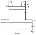
- a predetermined portion of the electrode 23 and the second conductivity type GaAs layer 9 are etched to reach the surface of the GaAs layer 8 so as to form a light-receiving portion of the photodiode.
- predetermined portions of the electrode 23, the second conductivity type GaAs layer 9, the GaAs layer 8, the GaInP layer 7, the GaInP active layer 5 and the first conductivity type GaInP buffer layer 3 are etched to produce the pin-type photodiode as shown in Figure 4.
- the sensitivity of the thus produced pin-type photodiode proved to be superior to that of a pin-type photodiode produced in the same method except excluding the step of radiating As molecular beams on the layer 7 and raising the substrate temperature to 620°C. This is because, according to the method of Example 4, formation of the surface state is reduced even on the surface where the layer growth is temporarily stopped.
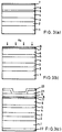
- Figure 5(d) is a sectional view of one example of the semiconductor laser device.
- the semiconductor laser device comprises a first conductivity type GaAs buffer layer 32, a first conductivity type GaInP buffer layer 33, a first conductivity type AlGaInP clad layer 34, a GaInP active layer 35, a second conductivity type AlGaInP clad layer 36, an (Al 0.7 Ga 0.3 ) 0.5 In 0.5 P first etching stop layer 37, a GaAs optical absorption layer 38 and an (Al 0.4 Ga 0.6 ) 0.5 In 0.5 P second etching stop layer 39 formed on a first conductivity type GaAs substrate 31 in this order.
- a stripe groove (5 pm width) is formed through the (Al 0.4 Ga 0.6 ) 0.5 In 0.5 P second etching stop layer 39 and the GaAs optical absorption layer 38 to reach the (Al 0.7 Ga 0.3 ) 0.5 In 0.5 P first etching stop layer 37.
- An Al 0.7 Ga 0.3 As layer 40 of a thickness of several molecules is formed on the surface of the first etching stop layer 37 exposed inside the stripe groove. Also, a Al 0.4 Ga 0.6 As layer 46 of a thickness of several molecules is formed on the surface of the second etching stop layer 39.
- a second conductivity type Al 0.7 Ga 0.3 As regrowing clad layer 41 is formed over the GaAs layer 38, the Al 0.7 Ga 0.3 As layer 40 and the Al 0.4 Ga 0.6 As layer 46 in such a manner that the stripe groove is filled up.
- the first conductivity type AlGaInP clad layer 34, the GaInP active layer 35 and the second conductivity type AlGaInP clad layer 36 constitute a double hetero structure, and therefore most light beams generated inside the active layer 35 are confined within this double hetero structure.
- the band gap energy in the GaAs layer 38 positioned on the both sides of the stripe groove is smaller than the energy of light beams generated in the active layer 35. Therefore, the GaAs layer 38 comparatively easily absorbs the light beams.
- the Al 0.7 Ga 0.3 As regrowing clad layer 41 is made to have a sufficiently large band gap and a sufficiently small refractive index required to confine the light beams generated in the active layer 35 within the double hetero structure. This results in producing an effective refractive index difference between the inside and the outside of the stripe groove formed above the double hetero structure, and thus the horizontal transverse mode of laser beams is unified.
- a second conductivity type GaAs cap layer 42 is formed on the second conductivity type Al 0.7 Ga 0.3 As regrowing clad layer 41, and electrodes 45 and 44 are formed on the surface of the second conductivity type GaAs cap layer 42 and on the back surface of the substrate 31, respectively.
- the first conductivity type GaAs buffer layer 32, the first conductivity type GaInP buffer layer 33, the first conductivity type AlGaInP clad layer 34, the GaInP active layer 35, the second conductivity type AlGaInP clad layer 36, the (Al 0.7 Ga 0.3 ) 0.5 In 0.5 P first etching stop layer 37, the GaAs optical absorption layer 38 and the (Al 0.4 Ga 0.6 ) 0.5 In 0.5 P second etching stop layer 39 are formed on the first conductivity type GaAs substrate 31 in such a manner that one layer is continuously grown on another in this order by the MBE method.
- the substrate temperature at this stage is in the range of about 480°C and about 570°C.
- the substrate 31 should not be moved outside the MBE apparatus to in order to keep the growing layers clean.
- the total thickness of the second conductivity type AlGaInP second clad layer 36 and the second conductivity type (Al 0.7 Ga 0.3 ) 0.5 In 0.5 P first etching stop layer 37 is as small as about 200 nm so that light beams generated in the active layer 35 can be transmitted to the GaAs optical absorption layer 38.
- the layered substrate is taken out of the MBE apparatus. Some portions of the (Al 0.4 Ga 0.6 ) 0.5 In 0.5 P second etching stop layer 39 and the GaAs optical absorption layer 38 are selectively etched using a photo mask 43 to form a stripe groove extending to reach the (Al 0.7 Ga 0.3 ) 0.5 In 0.5 P first etching stop layer 37 ( Figure 5(b)).
- impurities such as oxygen and steam in the atmosphere attach and contaminate the surface of the (Al 0.7 Ga 0.3 ) 0.5 In 0.5 P second conductivity type first etching stop layer 37.
- the contaminated surface of the layer 37 deteriorates the crystallinity of other layers to be grown thereon.
- the layered substrate is returned to the MBE apparatus where the layer 37 and the layer 39 are exposed to a sufficient amount of As molecular beams while the substrate temperature is raised to 620°C. The condition is maintained for several minutes.
- the Al 0.7 Ga 0.3 As layer 40 and the Al 0.4 Ga 0.6 As layer 46 formed in this step are thermally stable at a temperature below about 680°C, seldom causing evaporation of the composing elements. Thus, the evaporation of In and P from these layers 37 and 39 which is normally active at around 620°C can be avoided by being covered with these thin layers 40 and 46.
- the substrate temperature at radiation of As molecular beams is not limited to 620°C but can be about 580°C or higher at which In evaporates to form the Al 0.7 Ga 0.3 As layer 40 and the Al 0.4 Ga 0.6 As layer 46. P also evaporates in the temperature range where In evaporates. Therefore, both In and P are replaced with As under radiation of a sufficient amount of As molecular beams to form the layer 40 and the layer 46. At this time, in order to maintain the layer 40 and the layer 46 stable throughout the above stage, the substrate temperature is preferably about 680°C or lower.
- the second conductivity type Al 0.7 Ga 0.3 As regrowing clad layer 41 and the second conductivity type GaAs cap layer 42 are grown on the top surface of the layered substrate in such a manner that the stripe groove is filled up.
- the (Al 0.7 Ga 0.3 ) 0.5 In 0.5 P etching stop layer 37 and the (Al 0.4 Ga 0.6 ) 0.5 In 0.5 P etching stop layer 39 are significantly deteriorated caused by the evaporation of In and P therein at the temperature required to grow the second conductivity type regrowing clad layer 41.
- this deterioration can be avoided since these layers 37 and 39 are covered with the thermally stable Al 0.7 Ga 0.3 As layer 40 and Al 0.4 Ga 0.6 As layer 46, respectively.
- the Al 0.7 Ga 0.3 As regrowing clad layer 41 is formed to have a band gap energy greater than the energy of light beams generated in the active layer 35 by adjusting the Al content in the layer.
- the light beams generated in the active layer 35 can thus be confined within the double hetero structure.
- Electrodes 45 and 44 are formed on the top surface of the layered structure and on the back surface of the substrate 31, respectively, to produce the index guided semiconductor laser device as shown in Figure 5(d).
- the semiconductor laser device of this example comprising the double hetero structure including the AlGaInP crystal layers can continuously radiate light beams of a wavelength of 670 nm at room temperature.
- the index-guided semiconductor laser device having a stripe groove inside the device can radiate the laser beams of the unified horizontal transverse mode.
- the semiconductor laser device of this example is provided with the second conductivity type AlGaAs regrowing clad layer 41 including AlGaAs which has relatively high thermal conductivity, allowing heat generated in the active layer 35 to be efficiently diffused outside the semiconductor laser device.
- the semiconductor laser device of this example can show an excellent temperature property compared with the one shown in Figure 8.
- the (Al 0.7 Ga 0.3 ) 0.5 In 0.5 P layer 37 and the (Al 0.4 Ga 0.6 ) 0.5 In 0.5 P layer 39 were used as the etching stop layers.
- other composition ratio of AlGaInP than the above can also be used to form an AlGaInP etching stop layer which lattice-matches the substrate. This means that the lattice-matching with the substrate is possible for an etching stop layer formed of AlGalnP with an extensive variation of the composition ratio thereof, compared with, for example, AlGaAs.
- reduction of luminous efficiency caused by the failure in lattice-matching on the bottom portion of the stripe groove can be avoided, and laser beams of high optical output can be produced.
- the AlGaAs layer formed on the surface of the AlGaInP layer is not liable to be contaminated by impurities such as oxygen compared with, for example, an AlAs layer not including Ga.
- a semiconductor laser device was produced by the same method as described above but excluding the step of radiating As molecular beams and raising the substrate temperature to 620°C.
- the threshold current increased and therefore continuous oscillation at room temperature was not possible. This is because the surface of the second conductivity type AlGaInP first etching stop layer 37 was not purified and failed to grow a high quality AlGaAs regrowing clad layer 41 thereon.
- the Al 0.7 Ga 0.3 As layer 40 and the Al 0.4 Ga 0.6 As layer 46 being thin layers with a thickness of several molecules, do not give direct optical and electrical effects onto the properties of the semiconductor laser device.
- the semiconductor laser device of this example is provided with the(Al 0.4 Ga 0.6 ) 0.5 In 0.5 P layer as the second etching stop layer formed on the optical absorption layer 38.
- the crystallinity of the part of the AlGaAs regrowing layer 41 located above the optical absorption layer 38 then shows the same excellence as that of the part thereof grown above the stripe groove.
- the light beams generated in the active layer 35 are seldom transmitted into the part of the layer 41 located above the optical absorption layer 38, and therefore, a semiconductor laser device without the second etching stop layer 39 can obtain the same stable oscillation at room temperature as that of Example 5.
- Figure 6(d) is a sectional view of another example of a semiconductor laser device.
- the main differences between this example and Example 5 shown in Figure 5(d) are that in this example the (Al 0.4 Ga 0.6 ) 0.5 In 0.5 P layer is not formed on the optical absorption layer 38 and that on AlAs layer 49 is formed instead of the Al 0.7 Ga 0.3 As layer 40 of Example 5 on the etching stop layer in the bottom portion of the stripe groove.
- a first conductivity type GaAs buffer layer 32, a first conductivity type GaInP buffer layer 33, a first conductivity type AlGaInP first clad layer 34, a GaInP active layer 35, a second conductivity type AlGaInP second clad layer 36, an (Al 0.7 Ga 0.3 ) 0.5 In 0.5 P etching stop layer 37 and a GaAs optical absorption layer 38 are formed on a first conductivity type GaAs substrate 31 in such a manner that one layer is grown on another in this order by the MBE method.
- the total thickness of the second conductivity type AlGaInP second clad layer 36 and the second conductivity type (Al 0.7 Ga 0.3 ) 0.5 In 0.5 P etching stop layer 37 is as small as about 250 nm so that light beams generated in the active layer 35 can be transmitted to the GaAs optical absorption layer 38.
- the GaAs optical absorption layer 38 is selectively etched using a photo mask 43 to form a stripe groove with the depth not to reach the (Al 0.7 Ga 0.3 ) 0.5 In 0.5 P etching stop layer 37 ( Figure 6(b)), remaining an about 100 nm thick GaAs layer between the bottom surface of the stripe groove and the top surface of the etching stop layer 37.
- the layered substrate is returned to the MBE apparatus where the layered substrate 31 covered with the GaAs layer is exposed to a sufficient amount of As molecular beams while the substrate temperature is raised to 720°C. The condition is maintained for several minutes.
- the GaAs remaining in the bottom portion of the stripe groove evaporates, and Ga, In and P present near the surface of the resultantly exposed (Al 0.7 Ga 0.3 ) 0.5 In 0.5 P etching stop layer 37 are replaced with As in the As molecular beams, changing the portions near the surface of the layer 37 to an AlAs layer 49 of a thickness of several molecules ( Figure 6(c)).
- This thin AlAs layer 49 is thermally stable at about 720°C, not causing eminent evaporation of the composing elements. Thus, the evaporation of In and P from (Al 0.7 Ga 0.3 ) 0.5 In 0.5 P etching stop layer 37 which is normally active at around 720°C is avoided by being covered with this AlAs layer 49.
- the substrate temperature during the above step was 720°C, but in order to form the AlAs layer 49 it may be about 680°C or higher at which Ga and As evaporate. In and P also evaporate in the temperature range where Ga and As evaporate. Therefore, Ga, In and P present in the exposed portion of the (Al 0.7 Ga 0.3 ) 0.5 In 0.5 P layer 37 are replaced with As under radiation of a sufficient amount of As molecular beams to form the AlAs layer 49. At this time, in order to maintain the stability of the AlAs layer 49 throughout the above stage, the substrate temperature is preferably about 740°C or lower.
- the surface of the (Al 0.7 Ga 0.3 ) 0.5 In 0.5 P layer 37 is not exposed to the atmosphere, preventing it from being contaminated. Also, the surface of the GaAs layer contaminated by the exposition to the atmosphere can be purified by evaporating near the surface of the GaAs layer in the MBE apparatus.
- the AlAs layer 49 can prevent deterioration of the (Al 0.7 Ga 0.3 ) 0.5 In 0.5 P layer 37 caused by the evaporation of In and P which is normally active at a temperature about 580°C or higher.
- a second conductivity type Al 0.7 Ga 0.3 As regrowing clad layer 41 and a second conductivity type GaAs cap layer 42 are formed on the top surface of the layered substrate 31 in this order.
- the Al contain in the Al 0.7 Ga 0.3 As regrowing clad layer 41 is determined so that the refractive index is low enough to confine the light beams generated in the active layer 35 within the same layer 35.
- Electrodes 45 and 44 are formed on the top face of the multi-layered structure and on the back surface of the substrate 31, respectively, to produce the index-guided semiconductor laser device as shown in Figure 6(d).
- Figure 7(d) is a sectional view of a semiconductor laser device according to the present invention.
- the semiconductor laser device comprises a first conductivity type GaAs buffer layer 52, a first conductivity type GaInP buffer layer 53, a first conductivity type AlGaInP first clad layer 54, a GaInP active layer 55, a second conductivity type AlGaInP second clad layer 56 (150 nm thickness), a GaInP first etching stop layer 57 (7 nm thickness), a GaAs optical absorption layer 58 and a GaInP second etching stop layer 59 formed on a first conductivity type GaAs substrate 51 in this order.
- the first conductivity type AlGaInP first clad layer 54, the GaInP active layer 55 and the second conductivity type AlGaInP second clad layer 56 constitute a double hetero structure.
- a stripe groove (5 ⁇ m width) is formed through the GaInP second etching stop layer 59 and the GaAs optical absorption layer 58 to reach the surface of the GaInP first etching stop layer 57.
- a second conductivity type Al 0.7 Ga 0.3 As regrowing clad layer 61 is formed over the layered structure in such a manner that the stripe groove is filled up.
- the Al content in the Al 0.7 Ga 0.3 As regrowing clad layer 61 is determined so that the refractive index is low enough (about 3.3) to confine the light beams generated in the active layer 55 within the double hetero structure.
- the thermal conductivity of this regrowing clad layer 61 is about 0.1 W/cm ⁇ deg.
- Electrodes 65 and 64 are formed on the top surface of the cap layer 62 and the back surface of the substrate 51, respectively.
- the first conductivity type GaAs buffer layer 52, the first conductivity type GaInP buffer layer 53, the first conductivity type AlGaInP first clad layer 54, the GaInP active layer 55, the second conductivity type AlGaInP second clad layer 56, the GaInP first etching stop layer 57, the GaAs optical absorption layer 58 and the GaInP second etching stop layer 59 are formed on the first conductivity type GaAs substrate 51 in such a manner that one layer is grown on another in this order.
- the substrate temperature at growing the layers is in the range of about 450°C and about 570°C.
- the substrate 51 should not be moved outside the MBE apparatus in order to keep the growing layers clean.
- the thickness of the second conductivity type AlGaInP second clad layer 56 is as small as about 150 nm so that light beams generated in the active layer 55 can be transmitted to the GaAs optical absorption layer 58.
- impurities such as oxygen and steam in the atmosphere attach the surface of the GaInP first etching stop layer 57.
- the GaInP layers 57 and 59 are exposed to a sufficient amount of As molecular beams so as to purify the surfaces thereof while the substrate temperature is raised to 620°C. The condition is maintained for several minutes.
- the GaAs layer 60 is thermally stable seldom causing evaporation of composing elements at a temperature below about 680°C.
- the substrate temperature at the stage of forming the GaAs layer 60 is not limited to 620°C but can be about 580°C or higher at which In evaporates to form the GaAs layer 60. P also evaporates in the temperature range where In evaporates. Therefore, both In and P are replaced with As under radiation of a sufficient amount of As molecular beams to form the GaAs layer 60. At this time, in order to maintain the stability of the GaAs layer 60 throughout the above stage, the substrate temperature is preferably about 680°C or lower.
- the GaAs layer 60 by forming the GaAs layer 60, the deterioration of the GaInP layers 57 and 59 caused by evaporation of In and P therein which is especially eminent at a temperature of about 580°C or higher can be avoided at a temperature of about 680°C.
- a second conductivity type Al 0.7 Ga 0.3 As regrowing clad layer 61 and a second conductivity type GaAs cap layer 62 are grown on the top surface of the layered substrate in such a manner that the stripe groove is filled up.
- the GaAs layers 57 and 59 are significantly deteriorated caused by the evaporation of In and P therein at the temperature required to grow the Al 0.7 Ga 0.3 As regrowing clad layer 61. In this example, however, this deterioration can be avoided since these layers 57 and 59 are covered with the thermally stable GaAs layer 60.
- the Al 0.7 Ga 0.3 As regrowing clad layer 61 is formed to have a band gap energy (2.1 eV) greater than the energy of light beams (about 1.9 eV) generated in the active layer 55 by adjusting the Al content in the layer.
- the light beams generated in the active layer 55 can thus be confined within the double hetero structure.
- the band gap energy of the GaAs layer 58 having the stripe groove therethrough is smaller than the energy of light beams generated in the active layer 55, which light beams are therefore easily absorbed by the GaAs layer 58.
- the refractive indexes between the inside and the outside of the stripe groove located above the double hetero structure is produced, and thus the horizontal transverse mode of laser beams is unified.
- Electrodes 65 and 64 are formed on the top surface of the multi-layered structure and on the back surface of the substrate 51 to produce the index-guided semiconductor laser device as shown in Figure 7(d).
- the semiconductor laser device of this example can continuously radiate 670 nm wavelength light beams at room temperature, wherein the horizontal transverse mode of laser beams is unified.
- the GaAs layer 60 being a thin layer of a thickness of several molecules, does not directly give optical and electrical effects onto the properties of the semiconductor laser device.
- the semiconductor laser device of this example is provided with the second conductivity type AlGaAs regrowing clad layer 61 including AlGaAs which has relatively high thermal conductivity, allowing heat generated in the active layer 55 to be efficiently diffused outside the semiconductor laser device.
- the semiconductor laser device of this example can show an excellent temperature property compared with the one shown in Figure 8.
- a semiconductor laser device was produced by the same producing method described above but excluding the step of radiating As molecular beams and raising the substrate temperature to 620°C.
- the threshold current increased and continuous oscillation at room temperature was not possible. This is because the surface of the second conductivity type GaInP first etching stop layer 57 was not purified, failing in growing a high quality AlGaAs regrowing clad layer thereon.
- the semiconductor laser device of this example is provided with the GaInP layer as the second etching stop layer 59 formed on the GaAs layer 60.
- the crystallinity of the part of the AlGaAs regrowing layer 61 located above the optical absorption layer 58 then shows the same excellence as that of the part thereof grown above the stripe groove where the optical absorption layer 58 is removed.
- the light beams generated in the active layer 55 are seldom transmitted into the part of the layer 61 located above the optical absorption layer 58, and, therefore, a semiconductor laser device without the second etching stop layer 59 can obtain the same stable oscillation at room temperature as that of Example 7.
- the threshold current slightly increases. It is preferable therefore to also provide the GaInP second etching stop layer 59 on the optical absorption layer 58 so as to obtain a semiconductor laser device capable of stably oscillating at room temperature with the low threshold current.
- the GaInP first etching stop layer 57 of this example is 7 nm thick. It was found that a semiconductor laser device having the layer of a thickness of 20 nm failed to stably oscillate at room temperature. The reason is that when the thickness of the GaInP first etching stop layer 57 is large compared with the de Broglie wavelength, the optical absorption of the layer 57 increases, which increases the waveguide loss and therefore raises the threshold current.
- the thickness of the GaInP first etching stop layer 57 must be smaller than the electronic de Broglie wavelength. Practically, the thickness is preferably in the range of about 3 nm and about 15 nm.
- the band gap energy of the GaInP first etching stop layer 57 can be made greater than that of the active layer 55 by forming a quantum state in the layer 57, so as to reduce the optical absorption.
- the GaInP layer used as the etching stop layers which does not include the active Al has an advantage of being less contaminated by oxygen, steam and the like than the AlGaInP layer. Therefore, the semiconductor laser device of this example which has the GaInP etching stop layers disposed above the double hetero structure including AlGaInP layers is advantageous in being less contaminated during the producing process and also being capable of continuously oscillating visible light beams at room temperature.
- a layer made of GaAs was used as the optical absorption layer 58, but other materials which easily absorb the light beams generated in the active layer 55 such as AlGaAs may also be used.
- the double hetero structure are composed of the first conductivity type AlGaInP first clad layer, the GaInP active layer and the second conductivity type AlGaInP second clad layer.
- the structure may be formed of semiconductor layers of other compositions of the AlGaInP group: for example, layers formed of an AlInP three element mixed crystal as the first and the second clad layers, a layer formed of an AlGaInP four element mixed crystal as the active layer, or a layer having the quantum well structure or the superlattice structure can be used.
- An SCH structure can also be formed by providing between the clad layers and the active layer a guide which is small in gain and absorption loss.
Landscapes
- Engineering & Computer Science (AREA)
- Physics & Mathematics (AREA)
- Condensed Matter Physics & Semiconductors (AREA)
- General Physics & Mathematics (AREA)
- Microelectronics & Electronic Packaging (AREA)
- Computer Hardware Design (AREA)
- Power Engineering (AREA)
- Manufacturing & Machinery (AREA)
- Electromagnetism (AREA)
- Optics & Photonics (AREA)
- Geometry (AREA)
- Chemical & Material Sciences (AREA)
- Materials Engineering (AREA)
- Semiconductor Lasers (AREA)
- Physical Deposition Of Substances That Are Components Of Semiconductor Devices (AREA)
Claims (4)
- Procédé de production d'un dispositif laser à semiconducteur, comprenant les étapes :de formation sur un substrat de GaAs (51) d'une double hétérojonction composée de couches de cristaux de AlGaInP (53, 54, 55, 56) dont le réseau cristallin correspond à celui du substrat de GaAs;de formation d'une couche de GaInP d'arrêt d'attaque chimique (57) sur la double hétérojonction;de formation d'une couche d'absorption optique (58) destinée à absorber une lumière générée dans la couche active afin de stabiliser le mode transversal horizontal, sur la couche de GaInP d'arrêt d'attaque chimique;de formation d'une rainure en bande dans la couche d'absorption optique afin d'atteindra la couche d'arrêt d'attaque chimique (57);d'irradiation par des faisceaux de molécules de As de la couche de GaInP d'arrêt d'attaque chimique à l'intérieur de la rainure en bande dans un appareil de MBE, tandis que le substrat sur lequel sont formées les couches est chauffé jusqu'à une température à laquelle In et P de la couche de GaInP d'arrêt d'attaque chimique s'évaporent afin de transformer la partie de la couche de GaInP d'arrêt d'attaque chimique, située au niveau et à proximité de la surface supérieure de celle-ci qui a été irradiée par les faisceaux de molécules de As, en une couche de GaAs (60) ayant une épaisseur de plusieurs molécules; etde formation d'une couche de AlGaAs (61) sur la couche de GaAs et sur la couche d'absorption optique dans l'appareil de MBE, la couche de AlGaAs ayant une énergie de la bande interdite supérieure à l'énergie d'un photon généré à l'intérieur de la double hétérojonction.
- Méthode de production d'un dispositif laser à semiconducteur selon la revendication 1 et comprenant, en outre, l'étape de formation d'une seconde couche de GaInP d'arrêt d'attaque chimique (59) sur la couche d'absorption optique (58), et de formation de la rainure en bande par une attaque chimique sélective de la seconde couche de GaInP d'arrêt d'attaque chimique (69) et de la couche d'absorption optique (58) pour atteindra la première couche de GaInP d'arrêt d'attaque chimique (57); la seconde couche d'arrêt d'attaque chimique (59) étant irradiée pendant l'étape d'irradiation par des faisceaux de molécules de As afin que sa partie située au niveau et à proximité de sa surface supérieure qui a été irradiée par les faisceaux de molécules de As, soit transformée en une couche de GaAs (60) ayant une épaisseur de plusieurs molécules; et la couche de AlGaAs (61) étant formée sur la couche de GaAs (60).
- Dispositif laser à semiconducteur comprenant :un substrat de GaAs (51);une double hétérojonction formée sur le substrat de GaAs et composée de couches de cristaux de AlGaInP (53, 54, 55, 56) dont le réseau cristallin correspond à celui du substrat de GaAs;une couche d'absorption optique (58) destinée à absorber une lumière générée dans la couche active afin de stabiliser le mode transversal horizontal, et prévue sur la double hétérojonction, une rainure en bande s'étendant à travers la couche d'absorption optique; etune couche de AlGaAs (61) disposée sur la couche d'absorption optique et dans la rainure en bande, l'énergie de la bande interdite de la couche de AlGaAs étant supérieure à l'énergie d'un photon généré à l'intérieur de la double hétérojonction;le dispositif laser étant caractérisé en ce qu'il comprend, en outre, une couche de GaInP d'arrêt d'attaque chimique (57) formée sur la double hétérojonction, la couche d'absorption optique (58) étant formée sur la couche de GaInP d'arrêt d'attaque chimique et la rainure en bande s'étendant à travers la couche d'absorption optique pour atteindra la couche de GaInP d'arrêt d'attaque chimique, la partie de ladite couche de GaInP d'arrêt d'attaque chimique, située sous ladite rainure en bande au niveau et à proximité de la surface supérieure de ladite couche de GaInP d'arrêt d'attaque chimique, étant transformée en une couche de GaAs; et en ce que l'épaisseur de la couche de GaInP d'arrêt d'attaque chimique se situe dans la plage de 3 nm à 15 nm.
- Dispositif laser à semiconducteur selon la revendication 3, dans lequel une seconde couche de GaInP d'arrêt d'attaque chimique (59) est formée sur la couche d'absorption optique (58).
Priority Applications (1)
| Application Number | Priority Date | Filing Date | Title |
|---|---|---|---|
| EP97105580A EP0785603B1 (fr) | 1990-05-09 | 1991-05-09 | Dispositif laser à semiconducteur et méthode de fabrication |
Applications Claiming Priority (7)
| Application Number | Priority Date | Filing Date | Title |
|---|---|---|---|
| JP2120858A JP2537295B2 (ja) | 1990-05-09 | 1990-05-09 | 半導体レ―ザ素子及びその製造方法 |
| JP120858/90 | 1990-05-09 | ||
| JP129914/90 | 1990-05-18 | ||
| JP2129916A JP2533962B2 (ja) | 1990-05-18 | 1990-05-18 | 半導体レ―ザ素子及びその製造方法 |
| JP2129914A JPH0828326B2 (ja) | 1990-05-18 | 1990-05-18 | 化合物半導体層の製造方法 |
| JP129916/90 | 1990-05-18 | ||
| EP91304161A EP0456485B1 (fr) | 1990-05-09 | 1991-05-09 | Méthode de production d'un composant à semi-conducteur |
Related Parent Applications (2)
| Application Number | Title | Priority Date | Filing Date |
|---|---|---|---|
| EP91304161.2 Division | 1991-05-09 | ||
| EP91304161A Division EP0456485B1 (fr) | 1990-05-09 | 1991-05-09 | Méthode de production d'un composant à semi-conducteur |
Related Child Applications (1)
| Application Number | Title | Priority Date | Filing Date |
|---|---|---|---|
| EP97105580A Division EP0785603B1 (fr) | 1990-05-09 | 1991-05-09 | Dispositif laser à semiconducteur et méthode de fabrication |
Publications (2)
| Publication Number | Publication Date |
|---|---|
| EP0695006A1 EP0695006A1 (fr) | 1996-01-31 |
| EP0695006B1 true EP0695006B1 (fr) | 1998-03-04 |
Family
ID=27314128
Family Applications (3)
| Application Number | Title | Priority Date | Filing Date |
|---|---|---|---|
| EP95115775A Expired - Lifetime EP0695006B1 (fr) | 1990-05-09 | 1991-05-09 | Méthode de production d'un composé laser à semi-conducteur |
| EP91304161A Expired - Lifetime EP0456485B1 (fr) | 1990-05-09 | 1991-05-09 | Méthode de production d'un composant à semi-conducteur |
| EP97105580A Expired - Lifetime EP0785603B1 (fr) | 1990-05-09 | 1991-05-09 | Dispositif laser à semiconducteur et méthode de fabrication |
Family Applications After (2)
| Application Number | Title | Priority Date | Filing Date |
|---|---|---|---|
| EP91304161A Expired - Lifetime EP0456485B1 (fr) | 1990-05-09 | 1991-05-09 | Méthode de production d'un composant à semi-conducteur |
| EP97105580A Expired - Lifetime EP0785603B1 (fr) | 1990-05-09 | 1991-05-09 | Dispositif laser à semiconducteur et méthode de fabrication |
Country Status (3)
| Country | Link |
|---|---|
| US (2) | US5255279A (fr) |
| EP (3) | EP0695006B1 (fr) |
| DE (3) | DE69133230T2 (fr) |
Families Citing this family (14)
| Publication number | Priority date | Publication date | Assignee | Title |
|---|---|---|---|---|
| JP2706369B2 (ja) * | 1990-11-26 | 1998-01-28 | シャープ株式会社 | 化合物半導体の成長方法及び半導体レーザの製造方法 |
| JP2708992B2 (ja) * | 1991-12-20 | 1998-02-04 | シャープ株式会社 | AlGaInP系半導体発光装置の製造方法 |
| JPH07162089A (ja) * | 1993-12-13 | 1995-06-23 | Mitsubishi Electric Corp | 可視光レーザダイオード及びその製造方法 |
| TW291585B (fr) * | 1994-07-04 | 1996-11-21 | Mitsubishi Chem Corp | |
| US5656539A (en) * | 1994-07-25 | 1997-08-12 | Mitsubishi Denki Kabushiki Kaisha | Method of fabricating a semiconductor laser |
| US5656829A (en) * | 1994-08-30 | 1997-08-12 | Showa Denko K.K. | Semiconductor light emitting diode |
| US5787104A (en) * | 1995-01-19 | 1998-07-28 | Matsushita Electric Industrial Co., Ltd. | Semiconductor light emitting element and method for fabricating the same |
| JP3373386B2 (ja) * | 1997-03-19 | 2003-02-04 | 富士通株式会社 | 半導体装置及びその製造方法 |
| US6888175B1 (en) | 1998-05-29 | 2005-05-03 | Massachusetts Institute Of Technology | Compound semiconductor structure with lattice and polarity matched heteroepitaxial layers |
| US6803603B1 (en) * | 1999-06-23 | 2004-10-12 | Kabushiki Kaisha Toshiba | Semiconductor light-emitting element |
| CN1324719C (zh) * | 2004-04-01 | 2007-07-04 | 光磊科技股份有限公司 | 一种发光二极管 |
| FR2876841B1 (fr) * | 2004-10-19 | 2007-04-13 | Commissariat Energie Atomique | Procede de realisation de multicouches sur un substrat |
| US8692286B2 (en) * | 2007-12-14 | 2014-04-08 | Philips Lumileds Lighing Company LLC | Light emitting device with bonded interface |
| WO2009120044A2 (fr) * | 2008-03-27 | 2009-10-01 | Song June O | Élément électroluminescent et procédé de production correspondant |
Family Cites Families (15)
| Publication number | Priority date | Publication date | Assignee | Title |
|---|---|---|---|---|
| US4493142A (en) * | 1982-05-07 | 1985-01-15 | At&T Bell Laboratories | III-V Based semiconductor devices and a process for fabrication |
| JPS60192380A (ja) * | 1984-03-13 | 1985-09-30 | Mitsubishi Electric Corp | 半導体レ−ザ装置 |
| DE3683521D1 (de) * | 1985-04-02 | 1992-03-05 | Fujitsu Ltd | Thermisches aetzen eines verbindungshalbleiters. |
| JPH0728084B2 (ja) * | 1985-07-26 | 1995-03-29 | ソニー株式会社 | 半導体レーザー |
| JPS63104493A (ja) * | 1986-10-22 | 1988-05-09 | Nec Corp | 半導体レ−ザ素子 |
| US5068204A (en) * | 1987-03-27 | 1991-11-26 | Misawa Co. Ltd. | Method of manufacturing a light emitting element |
| JPS63284878A (ja) * | 1987-04-30 | 1988-11-22 | シーメンス、アクチエンゲゼルシヤフト | 埋込み活性層をもつレーザダイオードの製造方法 |
| JPS6437869A (en) * | 1987-08-03 | 1989-02-08 | Sanyo Electric Co | Solid-state image sensing device |
| JPS6437871A (en) * | 1987-08-04 | 1989-02-08 | Seiko Epson Corp | Solid-state image sensor |
| JPS6437873A (en) * | 1987-08-04 | 1989-02-08 | Hitachi Ltd | Semiconductor device and manufacture thereof |
| JPS6437870A (en) * | 1987-08-04 | 1989-02-08 | Seiko Epson Corp | Solid-state image sensing device and manufacture thereof |
| JPH01134985A (ja) * | 1987-11-19 | 1989-05-26 | Mitsubishi Electric Corp | 半導体レーザ装置 |
| JPH0828554B2 (ja) * | 1989-10-20 | 1996-03-21 | 三菱電機株式会社 | 半導体レーザ及びその製造方法 |
| US5058120A (en) * | 1990-02-28 | 1991-10-15 | Kabushiki Kaisha Toshiba | Visible light emitting semiconductor laser with inverse mesa-shaped groove section |
| JPH0513881A (ja) * | 1990-11-28 | 1993-01-22 | Matsushita Electric Ind Co Ltd | 半導体レーザの製造方法 |
-
1991
- 1991-05-09 DE DE69133230T patent/DE69133230T2/de not_active Expired - Fee Related
- 1991-05-09 DE DE69120865T patent/DE69120865T2/de not_active Expired - Fee Related
- 1991-05-09 DE DE69129047T patent/DE69129047T2/de not_active Expired - Fee Related
- 1991-05-09 EP EP95115775A patent/EP0695006B1/fr not_active Expired - Lifetime
- 1991-05-09 US US07/698,001 patent/US5255279A/en not_active Expired - Lifetime
- 1991-05-09 EP EP91304161A patent/EP0456485B1/fr not_active Expired - Lifetime
- 1991-05-09 EP EP97105580A patent/EP0785603B1/fr not_active Expired - Lifetime
-
1993
- 1993-06-21 US US08/080,004 patent/US5360762A/en not_active Expired - Lifetime
Also Published As
| Publication number | Publication date |
|---|---|
| DE69129047D1 (de) | 1998-04-09 |
| DE69120865T2 (de) | 1997-01-23 |
| US5255279A (en) | 1993-10-19 |
| DE69133230T2 (de) | 2003-12-11 |
| EP0785603B1 (fr) | 2003-04-02 |
| EP0456485A3 (en) | 1992-04-15 |
| EP0785603A2 (fr) | 1997-07-23 |
| EP0456485A2 (fr) | 1991-11-13 |
| EP0695006A1 (fr) | 1996-01-31 |
| US5360762A (en) | 1994-11-01 |
| EP0456485B1 (fr) | 1996-07-17 |
| DE69120865D1 (de) | 1996-08-22 |
| DE69129047T2 (de) | 1998-09-03 |
| DE69133230D1 (de) | 2003-05-08 |
| EP0785603A3 (fr) | 1997-11-26 |
Similar Documents
| Publication | Publication Date | Title |
|---|---|---|
| US6563851B1 (en) | Laser diode having an active layer containing N and operable in a 0.6 μm wavelength band | |
| US6590919B1 (en) | Nitride group compound semiconductor laser device and method for producing the same | |
| EP0695006B1 (fr) | Méthode de production d'un composé laser à semi-conducteur | |
| US7384479B2 (en) | Laser diode having an active layer containing N and operable in a 0.6 μm wavelength | |
| JPH06302906A (ja) | 半導体レーザ及びその製造方法 | |
| JP3585817B2 (ja) | レーザダイオードおよびその製造方法 | |
| EP1006629A2 (fr) | Dispositif émetteur de lumière à semi-conducteur composé | |
| US7088755B2 (en) | Nitride-base semiconductor laser device | |
| US6055257A (en) | Quantum cascade laser | |
| US5588016A (en) | Semiconductor laser device | |
| US5270246A (en) | Manufacturing method of semiconductor multi-layer film and semiconductor laser | |
| US6884291B1 (en) | Laser diode having an active layer containing N and operable in a 0.6 μm wavelength band | |
| EP0915542B1 (fr) | Laser à semiconducteur avec des couches de blocage du courant améliorées et méthode de fabrication | |
| JP2624881B2 (ja) | 半導体レーザ素子およびその製造方法 | |
| JP2003008147A (ja) | 半導体レーザ素子及びその製造方法 | |
| EP1035624B1 (fr) | Laser à semiconducteur et méthode de fabrication | |
| JP2909144B2 (ja) | 半導体レーザ装置及びその製造方法 | |
| JP2533962B2 (ja) | 半導体レ―ザ素子及びその製造方法 | |
| JP4192293B2 (ja) | AlGaAs系半導体レーザの製造方法、AlGaAs系半導体装置の製造方法および化合物半導体の成長方法 | |
| JP2664794B2 (ja) | 半導体レーザ素子の製造方法 | |
| JP2780625B2 (ja) | 半導体レーザの製造方法 | |
| KR100363240B1 (ko) | 반도체 레이저 다이오드 및 그 제조방법 | |
| JP2537295B2 (ja) | 半導体レ―ザ素子及びその製造方法 | |
| JPS6016488A (ja) | 半導体レ−ザ装置 | |
| JPH0669593A (ja) | 半導体レーザ装置 |
Legal Events
| Date | Code | Title | Description |
|---|---|---|---|
| PUAI | Public reference made under article 153(3) epc to a published international application that has entered the european phase |
Free format text: ORIGINAL CODE: 0009012 |
|
| 17P | Request for examination filed |
Effective date: 19951019 |
|
| AC | Divisional application: reference to earlier application |
Ref document number: 456485 Country of ref document: EP |
|
| AK | Designated contracting states |
Kind code of ref document: A1 Designated state(s): DE FR GB |
|
| 17Q | First examination report despatched |
Effective date: 19960607 |
|
| GRAG | Despatch of communication of intention to grant |
Free format text: ORIGINAL CODE: EPIDOS AGRA |
|
| RIN1 | Information on inventor provided before grant (corrected) |
Inventor name: MATSUI, SADAYOSHI Inventor name: SUYAMA, TAKAHIRO Inventor name: TSUNODA, ATSUO Inventor name: HOSODA, MASAHIRO Inventor name: TAKAHASHI, KOSEI |
|
| GRAG | Despatch of communication of intention to grant |
Free format text: ORIGINAL CODE: EPIDOS AGRA |
|
| GRAG | Despatch of communication of intention to grant |
Free format text: ORIGINAL CODE: EPIDOS AGRA |
|
| GRAH | Despatch of communication of intention to grant a patent |
Free format text: ORIGINAL CODE: EPIDOS IGRA |
|
| GRAH | Despatch of communication of intention to grant a patent |
Free format text: ORIGINAL CODE: EPIDOS IGRA |
|
| GRAA | (expected) grant |
Free format text: ORIGINAL CODE: 0009210 |
|
| AC | Divisional application: reference to earlier application |
Ref document number: 456485 Country of ref document: EP |
|
| AK | Designated contracting states |
Kind code of ref document: B1 Designated state(s): DE FR GB |
|
| XX | Miscellaneous (additional remarks) |
Free format text: TEILANMELDUNG 97105580.1 EINGEREICHT AM 04/04/97. |
|
| REF | Corresponds to: |
Ref document number: 69129047 Country of ref document: DE Date of ref document: 19980409 |
|
| ET | Fr: translation filed | ||
| PLBE | No opposition filed within time limit |
Free format text: ORIGINAL CODE: 0009261 |
|
| STAA | Information on the status of an ep patent application or granted ep patent |
Free format text: STATUS: NO OPPOSITION FILED WITHIN TIME LIMIT |
|
| 26N | No opposition filed | ||
| PGFP | Annual fee paid to national office [announced via postgrant information from national office to epo] |
Ref country code: DE Payment date: 20010430 Year of fee payment: 11 |
|
| PGFP | Annual fee paid to national office [announced via postgrant information from national office to epo] |
Ref country code: GB Payment date: 20010509 Year of fee payment: 11 |
|
| PGFP | Annual fee paid to national office [announced via postgrant information from national office to epo] |
Ref country code: FR Payment date: 20010518 Year of fee payment: 11 |
|
| REG | Reference to a national code |
Ref country code: GB Ref legal event code: IF02 |
|
| PG25 | Lapsed in a contracting state [announced via postgrant information from national office to epo] |
Ref country code: GB Free format text: LAPSE BECAUSE OF NON-PAYMENT OF DUE FEES Effective date: 20020509 |
|
| PG25 | Lapsed in a contracting state [announced via postgrant information from national office to epo] |
Ref country code: DE Free format text: LAPSE BECAUSE OF NON-PAYMENT OF DUE FEES Effective date: 20021203 |
|
| GBPC | Gb: european patent ceased through non-payment of renewal fee |
Effective date: 20020509 |
|
| PG25 | Lapsed in a contracting state [announced via postgrant information from national office to epo] |
Ref country code: FR Free format text: LAPSE BECAUSE OF NON-PAYMENT OF DUE FEES Effective date: 20030131 |
|
| REG | Reference to a national code |
Ref country code: FR Ref legal event code: ST |