EP0689374B1 - Elektronikmodul - Google Patents
Elektronikmodul Download PDFInfo
- Publication number
- EP0689374B1 EP0689374B1 EP95106186A EP95106186A EP0689374B1 EP 0689374 B1 EP0689374 B1 EP 0689374B1 EP 95106186 A EP95106186 A EP 95106186A EP 95106186 A EP95106186 A EP 95106186A EP 0689374 B1 EP0689374 B1 EP 0689374B1
- Authority
- EP
- European Patent Office
- Prior art keywords
- cover
- circuit board
- electronic module
- components
- cooling
- Prior art date
- Legal status (The legal status is an assumption and is not a legal conclusion. Google has not performed a legal analysis and makes no representation as to the accuracy of the status listed.)
- Expired - Lifetime
Links
Images

Classifications
-
- B—PERFORMING OPERATIONS; TRANSPORTING
- B60—VEHICLES IN GENERAL
- B60R—VEHICLES, VEHICLE FITTINGS, OR VEHICLE PARTS, NOT OTHERWISE PROVIDED FOR
- B60R16/00—Electric or fluid circuits specially adapted for vehicles and not otherwise provided for; Arrangement of elements of electric or fluid circuits specially adapted for vehicles and not otherwise provided for
- B60R16/02—Electric or fluid circuits specially adapted for vehicles and not otherwise provided for; Arrangement of elements of electric or fluid circuits specially adapted for vehicles and not otherwise provided for electric constitutive elements
- B60R16/023—Electric or fluid circuits specially adapted for vehicles and not otherwise provided for; Arrangement of elements of electric or fluid circuits specially adapted for vehicles and not otherwise provided for electric constitutive elements for transmission of signals between vehicle parts or subsystems
- B60R16/0239—Electronic boxes
-
- H—ELECTRICITY
- H05—ELECTRIC TECHNIQUES NOT OTHERWISE PROVIDED FOR
- H05K—PRINTED CIRCUITS; CASINGS OR CONSTRUCTIONAL DETAILS OF ELECTRIC APPARATUS; MANUFACTURE OF ASSEMBLAGES OF ELECTRICAL COMPONENTS
- H05K3/00—Apparatus or processes for manufacturing printed circuits
- H05K3/30—Assembling printed circuits with electric components, e.g. with resistors
- H05K3/32—Assembling printed circuits with electric components, e.g. with resistors electrically connecting electric components or wires to printed circuits
- H05K3/34—Assembling printed circuits with electric components, e.g. with resistors electrically connecting electric components or wires to printed circuits by soldering
- H05K3/3405—Edge mounted components, e.g. terminals
-
- H—ELECTRICITY
- H05—ELECTRIC TECHNIQUES NOT OTHERWISE PROVIDED FOR
- H05K—PRINTED CIRCUITS; CASINGS OR CONSTRUCTIONAL DETAILS OF ELECTRIC APPARATUS; MANUFACTURE OF ASSEMBLAGES OF ELECTRICAL COMPONENTS
- H05K5/00—Casings, cabinets or drawers for electric apparatus
- H05K5/0026—Casings, cabinets or drawers for electric apparatus provided with connectors and printed circuit boards [PCB], e.g. automotive electronic control units
- H05K5/0039—Casings, cabinets or drawers for electric apparatus provided with connectors and printed circuit boards [PCB], e.g. automotive electronic control units having a tubular housing wherein the PCB is inserted longitudinally
-
- H—ELECTRICITY
- H05—ELECTRIC TECHNIQUES NOT OTHERWISE PROVIDED FOR
- H05K—PRINTED CIRCUITS; CASINGS OR CONSTRUCTIONAL DETAILS OF ELECTRIC APPARATUS; MANUFACTURE OF ASSEMBLAGES OF ELECTRICAL COMPONENTS
- H05K1/00—Printed circuits
- H05K1/02—Details
- H05K1/0201—Thermal arrangements, e.g. for cooling, heating or preventing overheating
- H05K1/0203—Cooling of mounted components
-
- H—ELECTRICITY
- H05—ELECTRIC TECHNIQUES NOT OTHERWISE PROVIDED FOR
- H05K—PRINTED CIRCUITS; CASINGS OR CONSTRUCTIONAL DETAILS OF ELECTRIC APPARATUS; MANUFACTURE OF ASSEMBLAGES OF ELECTRICAL COMPONENTS
- H05K2201/00—Indexing scheme relating to printed circuits covered by H05K1/00
- H05K2201/10—Details of components or other objects attached to or integrated in a printed circuit board
- H05K2201/10007—Types of components
- H05K2201/10166—Transistor
-
- H—ELECTRICITY
- H05—ELECTRIC TECHNIQUES NOT OTHERWISE PROVIDED FOR
- H05K—PRINTED CIRCUITS; CASINGS OR CONSTRUCTIONAL DETAILS OF ELECTRIC APPARATUS; MANUFACTURE OF ASSEMBLAGES OF ELECTRICAL COMPONENTS
- H05K2201/00—Indexing scheme relating to printed circuits covered by H05K1/00
- H05K2201/10—Details of components or other objects attached to or integrated in a printed circuit board
- H05K2201/10007—Types of components
- H05K2201/10189—Non-printed connector
-
- H—ELECTRICITY
- H05—ELECTRIC TECHNIQUES NOT OTHERWISE PROVIDED FOR
- H05K—PRINTED CIRCUITS; CASINGS OR CONSTRUCTIONAL DETAILS OF ELECTRIC APPARATUS; MANUFACTURE OF ASSEMBLAGES OF ELECTRICAL COMPONENTS
- H05K2201/00—Indexing scheme relating to printed circuits covered by H05K1/00
- H05K2201/20—Details of printed circuits not provided for in H05K2201/01 - H05K2201/10
- H05K2201/2018—Presence of a frame in a printed circuit or printed circuit assembly
-
- H—ELECTRICITY
- H05—ELECTRIC TECHNIQUES NOT OTHERWISE PROVIDED FOR
- H05K—PRINTED CIRCUITS; CASINGS OR CONSTRUCTIONAL DETAILS OF ELECTRIC APPARATUS; MANUFACTURE OF ASSEMBLAGES OF ELECTRICAL COMPONENTS
- H05K3/00—Apparatus or processes for manufacturing printed circuits
- H05K3/30—Assembling printed circuits with electric components, e.g. with resistors
- H05K3/32—Assembling printed circuits with electric components, e.g. with resistors electrically connecting electric components or wires to printed circuits
- H05K3/34—Assembling printed circuits with electric components, e.g. with resistors electrically connecting electric components or wires to printed circuits by soldering
- H05K3/3465—Application of solder
- H05K3/3468—Application of molten solder, e.g. dip soldering
Definitions
- the invention relates to an electronic module according to the preamble of claim 1.
- Such an electronic module is due to the ABS / ASR-C electronics from WABCO Westinghouse Vehicle brakes known. With the previously known However, the problem arises that device to its Manufacturing requires several process steps are. In a first step, the Printed circuit board with components and the cooling element stocked. This is followed by a second process step in which the printed circuit board in the solder bath is soldered. In a third step the lid is attached to the circuit board and the heat-conducting connection between the cooling element and lid made.
- the invention is therefore based on the object an electronic module of the type mentioned above to further develop that the manufacture is simplified and is cheaper.
- An advantage of the invention is that the Cover with others before soldering Components are attached to the circuit board can. This leads to a separate assembly step for attaching the lid to the Printed circuit board after the solder bath is omitted.
- the invention is in a circuit board, at least one of the components as a heat-generating power component is formed and a cooling element for cooling the power component that Cooling element formed in one piece with the lid.
- This development of the invention has the advantage on that the heat conduction between the heat-generating Power component on the one hand and the Cooling element on the other hand and finally the heat emitting Lid is significantly improved. If on the other hand, the cooling element and the lid as separate Components are formed, it happens when attaching the cooling element to the lid unavoidable minimal air gaps that represent high heat transfer resistances and Heat dissipation between the cooling frame and lid significantly affect.
- the lid has recesses for receiving at least of a connector, the connector connectable on the outside of the cover and Inside the cover with the conductor tracks of the circuit board connected is.
- the lid, the circuit board and the im Cover picked connector by means of at least a connecting element penetrating all these parts connected with each other.
- the invention and the further developments described the invention can be particularly advantageous also use in motor vehicles. This in particular because in motor vehicles the space constraints for electronic modules are and in these cramped conditions a comparatively high power loss of the power components must be dissipated.
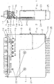
- FIG. 1 shows a side view of a housing pot (1) with internal pushing and holding elements (2), one with at least one is relatively strong heating power component (3) assembled circuit board (4) and a cover (5).
- the housing pot (1) is designed as a cuboid hollow body made of thermally conductive Material, especially metal, formed.
- the cover (5) is used as a heat sink in FIG. 3 shown recesses (9) to the circuit board (4) are directionally open on one side, designed, in the connector shown in Fig. 3 (8) are adjustable.
- the connector (8) can be attached to the cover (5).
- the lid (5) has shown in Fig. 2 Molded on the outside of the cover and on the inside of the cover Cooling elements (10) and (11) made of thermally conductive materials.
- the cover (5) with the fitted connectors (8) is load-bearing on a component Side surface (12) of the circuit board (4) on in Fig. 2 shown lid-side edge portion (13) put on and fastened.
- the attachment can be done in such a way that the cover (5), the fitted connector (8) and with Power components (3) printed circuit board (4) connected by means of one or more screws (14) being, with one screw all mentioned Penetrates parts. That is, the lid (5) that Connector (8) and the circuit board (4) with the same screws (14) connected.
- the cover (5) has a parallel to the printed circuit board (4) which is penetrated by the screw (14). This screwing of the parts mentioned into one Assembly (3, 4, 5, 8, 14) brings assembly advantages.
- the connector (8) and the circuit board (4) can also be used that penetrate the parts mentioned.
- press-in pins such.
- B. Grooved pins or pen-like spring elements such as Adapter sleeves or spiral dowel pins called. at Use of pin-like connecting elements can the cover (5), the connector (8) and the circuit board (4) with its complete Equipped with the help of the pen-like Connection element to a structural unit (3, 4, 5, 8, 14) and the structural unit (3, 4, 5, 8, 14) can then be passed over the solder bath become.
- solderable pin-like connecting element on the other hand, by soldering firmly with the solderable bath Side surface (18) of the board (4) connected become.
- a special modification of pin-like connecting elements can consist in on the cover (5) on the circuit board facing side in one piece with the cover Mold the pin as a pin.
- This pin serves to connect the cover of the connector (8) and the circuit board (4) a unit (3, 4, 5, 8, 14), which then like described above, in the solder bath by soldering with the board (4) can be connected.
- the connectors (8) are on the outside of the cover connectable and inside the cover via contact connections (15) on conductor tracks of the circuit board (4) connected.
- a close contact between the contact surfaces a cooling element (11) and a power component (3) can by the tension of a bracket (16), which comprises both elements (3) and (11) be what the heat dissipation from the Power components (3) promotes.
- the power components (3) are mostly transistors, but also resistors and Voltage regulators and other components can generate a high level of heat loss when electricity is passed through. Even microprocessors that are not directly using Contact can be cooled, generate heat loss and contribute to the build-up of heat.
- the on the lid-side edge portion (13) on the Front edge (17) of the circuit board (4) performed Attachment of the cover (5) to the power components load-bearing side surface (12) of the circuit board (4) without overhang of the cover (5) to the opposite side that can be soldered (18) of the circuit board (4) allows the assembly (3, 4, 5, 8, 14) in an advantageous manner to lead over a wave solder bath.
- Auxiliary bracket for pre-fixing the Power components are dispensed with. It does not apply also those required for the auxiliary brackets Assembly steps.
- the bracket (16) improves the Fixation by causing the Power components (3) flat and without an air gap touch the cooling element (11) on the inside of the cover.
- the housing pot (1) contains the inside of the in Fig. 2 shown narrow side walls (20) and (21) thrust guide and holding elements (2) z. B. designed in the form of guide channels could be.
- the housing pot (1) contains the inside of the in Fig. 2 shown narrow side walls (20) and (21) thrust guide and holding elements (2) z. B. designed in the form of guide channels could be.
- an opening (6) remains between the solderable side surface (18) of the circuit board (4) and the broad side wall (23), the either stay open or by a simple one Auxiliary cover (7) can be covered.
- This additional auxiliary cover does not have to be made of heat-conducting Material exist and does not have to other functions such as holding (fixing etc.) fulfill.
- the auxiliary cover can be considered a simple one Aperture to be executed and after assembly the assembly (3, 4, 5, 8, 14) with the housing pot (1) are placed on the opening (6).
- cooling elements (25) available on the housing pot (1) outside the Molded bottom wall (19) of the housing pot (1) are.
- the cooling elements designed as cooling fins (25) advantageously support the Reduction of the heat build-up in the housing pot in particular when there are several electronic modules in the vehicle are closely packed, and between them or on their wide side walls no convection is possible.
- the housing pot (1) made of a simple, non-heat conductive material (e.g. plastic) and it does not have to Have more cooling elements (25).
- the cover (5) can be die-cast be produced as a die-cast part.
Landscapes
- Engineering & Computer Science (AREA)
- Microelectronics & Electronic Packaging (AREA)
- Manufacturing & Machinery (AREA)
- Mechanical Engineering (AREA)
- Cooling Or The Like Of Electrical Apparatus (AREA)
- Casings For Electric Apparatus (AREA)
- Mounting Of Printed Circuit Boards And The Like (AREA)
Description
- Fig. 1
- ein erfindungsgemäßes Elektronikmodul in Seitenansicht mit Teilschnitt
- Fig. 2
- das Elektronikmodul nach Fig. 1 in der Draufsicht mit Teilschnitt und
- Fig. 3
- die Perspektivansicht des Elektronikmoduls nach Fig. 1.
- 1
- Gehäusetopf
- 2
- Schubführungs- und Halteelement
- 3
- Leistungsbauteil
- 4
- Leiterplatte
- 5
- Deckel
- 6
- Öffnung
- 7
- Hilfsabdeckung
- 8
- Anschlußstecker
- 9
- Aussparung
- 10
- Kühlelement, deckelaußenseitig
- 11
- Kühlelement, deckelinnenseitig
- 12
- bestückte Seitenfläche
- 13
- deckelseitiger Randabschnitt
- 14
- Schraube
- 15
- Kontaktanschluß
- 16
- Klammer
- 17
- Stirnkante
- 18
- lötbadfähige Seitenfläche
- 19
- Bodenwand
- 20
- schmalflächige Seitenwand
- 21
- schmalflächige Seitenwand
- 22
- Schraubverbindung
- 23
- breitflächige Seitenwand
- 24
- breitflächige Seitenwand
- 25
- Kühlelement, bodenwandaußenseitig
Claims (5)
- Elektronikmodul mit einem Gehäusetopf (1) zur Aufnahme mindestens einer mit Bauteilen bestückten Leiterplatte (4) und einem Deckel (5), mit folgenden Merkmalen:dadurch gekennzeichnet, daß der Deckel (5) nicht über die Lötseite (18) der Leiterplatte (4) hinausragt.a) der Gehäusetopf (1) ist als einseitig offen gestalteter, quaderförmiger Hohlkörper ausgebildet,b) der Deckel (5) ist mit der Leiterplatte (4) an deren deckelseitigem Randabschnitt (13) verbunden,
- Elektronikmodul nach Patentanspruch 1 für eine Leiterplatte (4), bei der wenigstens eines der Bauteile als wärmeerzeugendes Leistungsbauteil (3) ausgebildet ist und die ein Kühlelement (10, 11) zur Kühlung des Leistungsbauteils (3) trägt,
dadurch gekennzeichnet, daß das Kühlelement (10, 11) einstückig mit dem Deckel (5) ausgebildet ist. - Elektronikmodul nach Patentanspruch 1 oder 2,
dadurch gekennzeichnet, daß der Deckel (5) Aussparungen (9) zur Aufnahme wenigstens eines Anschlußsteckers (8) aufweist und daß der Anschlußstecker (8) deckelaußenseitig anschlußfähig und deckelinnenseitig mit den Leiterbahnen der Leiterplatte (4) verbunden ist. - Elektronikmodul nach Patentanspruch 3,
dadurch gekennzeichnet, daß der Deckel (5), die Leiterplatte (4) und der im Deckel (5) aufgenommene Anschlußstecker (8) mindestens mittels wenigstens eines alle genannten Teile durchdringenden Verbindungselementes (14) verbunden sind. - Elektronikmodul nach wenigstens einem der vorhergehenden Patentansprüche,
dadurch gekennzeichnet, daß der Deckel (5) als ein Druckgußteil ausgebildet ist.
Applications Claiming Priority (2)
| Application Number | Priority Date | Filing Date | Title |
|---|---|---|---|
| DE4422113 | 1994-06-24 | ||
| DE4422113A DE4422113C2 (de) | 1994-06-24 | 1994-06-24 | Elektronikmodul |
Publications (4)
| Publication Number | Publication Date |
|---|---|
| EP0689374A2 EP0689374A2 (de) | 1995-12-27 |
| EP0689374A3 EP0689374A3 (de) | 1997-11-05 |
| EP0689374B1 true EP0689374B1 (de) | 2003-03-05 |
| EP0689374B2 EP0689374B2 (de) | 2009-07-29 |
Family
ID=6521399
Family Applications (1)
| Application Number | Title | Priority Date | Filing Date |
|---|---|---|---|
| EP95106186A Expired - Lifetime EP0689374B2 (de) | 1994-06-24 | 1995-04-26 | Elektronikmodul |
Country Status (4)
| Country | Link |
|---|---|
| US (1) | US5712765A (de) |
| EP (1) | EP0689374B2 (de) |
| JP (1) | JP3790933B2 (de) |
| DE (2) | DE4422113C2 (de) |
Families Citing this family (22)
| Publication number | Priority date | Publication date | Assignee | Title |
|---|---|---|---|---|
| JP2954902B2 (ja) * | 1997-05-29 | 1999-09-27 | ファナック株式会社 | 制御用電子機器を内蔵した制御装置 |
| JP3248480B2 (ja) * | 1998-01-22 | 2002-01-21 | 住友電装株式会社 | 配電ボックス |
| DE19830227A1 (de) | 1998-07-07 | 2000-01-13 | Trw Automotive Electron & Comp | Gehäuse für eine Elektronik-Einheit, insbesondere für ein Airbag-Steuergerät |
| DE19911990A1 (de) * | 1999-03-17 | 2000-09-28 | Trw Automotive Electron & Comp | Metallgehäuse, insbesondere für ein Airbag-Steuergerät |
| DE19911989C2 (de) * | 1999-03-17 | 2003-04-24 | Trw Automotive Electron & Comp | Metallgehäuse |
| DE19941690C2 (de) | 1999-09-01 | 2001-12-06 | Siemens Ag | Steuergerät und Lötverfahren |
| JP3958589B2 (ja) * | 2002-01-23 | 2007-08-15 | 株式会社オートネットワーク技術研究所 | 電気接続箱 |
| JP4211580B2 (ja) * | 2003-11-18 | 2009-01-21 | 株式会社デンソー | 電子装置の筐体構造 |
| US7082034B2 (en) * | 2004-04-01 | 2006-07-25 | Bose Corporation | Circuit cooling |
| US6977337B1 (en) | 2004-06-16 | 2005-12-20 | Visteon Global Technologies, Inc. | Electronic assembly packaging |
| US7190589B2 (en) * | 2004-10-19 | 2007-03-13 | Cinch Connectors, Inc. | Electronic control enclosure |
| US7479020B2 (en) * | 2004-11-22 | 2009-01-20 | Visteon Global Technologies, Inc. | Electronic control module having an internal electric ground |
| CN2792121Y (zh) * | 2005-04-15 | 2006-06-28 | 鸿富锦精密工业(深圳)有限公司 | 主机板遮蔽架及具主机板遮蔽架的电子设备 |
| JP4694514B2 (ja) * | 2007-02-08 | 2011-06-08 | トヨタ自動車株式会社 | 半導体素子の冷却構造 |
| DE102007025957A1 (de) * | 2007-06-04 | 2008-12-11 | Robert Bosch Gmbh | Verfahren und Vorrichtung zum Festlegen eines eine elektrische Schaltung oder dergleichen aufweisenden Flächensubstrats in einer Einbauposition |
| US8238349B2 (en) * | 2008-06-18 | 2012-08-07 | Altera Canada Co. | Method of accessing stored information in multi-framed data transmissions |
| DE102009054767A1 (de) * | 2009-12-16 | 2011-06-22 | Robert Bosch GmbH, 70469 | Abschlusselement für ein Gehäuse |
| DE102012204145A1 (de) * | 2012-03-16 | 2013-09-19 | Continental Automotive Gmbh | Gehäuseblende zur Aufnahme von Steckermodulen |
| US9049811B2 (en) | 2012-11-29 | 2015-06-02 | Bose Corporation | Circuit cooling |
| JP6194868B2 (ja) * | 2014-09-18 | 2017-09-13 | 株式会社オートネットワーク技術研究所 | 電気接続箱 |
| JP6537700B2 (ja) * | 2016-03-04 | 2019-07-03 | 三菱電機株式会社 | 電装品モジュール及び空気調和機の室外機 |
| DE102019205715A1 (de) * | 2019-04-18 | 2020-10-22 | Robert Bosch Gmbh | Gehäuse zur Aufnahme von wärmeerzeugenden Bauteilen und Verwendung des Gehäuses |
Family Cites Families (28)
| Publication number | Priority date | Publication date | Assignee | Title |
|---|---|---|---|---|
| DE2546334C2 (de) * | 1975-10-16 | 1984-10-11 | Robert Bosch Gmbh, 7000 Stuttgart | Elektronisches Steuergerät |
| DE7709621U1 (de) * | 1977-03-26 | 1977-07-07 | Robert Bosch Gmbh, 7000 Stuttgart | Elektronisches Steuergerät |
| DE3041546C2 (de) * | 1980-11-04 | 1983-11-03 | Siemens AG, 1000 Berlin und 8000 München | Gehäuse zur Unterbringung mehrerer Baugruppen der Nachrichtentechnik |
| US4441140A (en) * | 1980-11-20 | 1984-04-03 | Raytheon Company | Printed circuit board holder |
| DE3225627C2 (de) * | 1982-07-08 | 1984-08-09 | Siemens AG, 1000 Berlin und 8000 München | Flachgehäuse für ein Funkgerät |
| DE3310477A1 (de) * | 1982-07-17 | 1984-01-19 | Robert Bosch Gmbh, 7000 Stuttgart | Elektrisches geraet, insbesondere schalt- und steuergeraet fuer kraftfahrzeuge |
| DE8318781U1 (de) * | 1983-06-29 | 1984-07-12 | Triumph-Adler Aktiengesellschaft für Büro- und Informationstechnik, 8500 Nürnberg | Gehäuse für ein elektronisches Steuergerät, insbesondere für Kraftfahrzeuge |
| US4546407A (en) * | 1983-10-31 | 1985-10-08 | Salvatore Benenati | Heat exchanging electronic module housing |
| US4557225A (en) * | 1984-01-18 | 1985-12-10 | Mikuni Kogyo Kabushiki Kaisha | Combined housing and heat sink for electronic engine control system components |
| US4516189A (en) * | 1984-02-29 | 1985-05-07 | Johnson Service Company | Control apparatus having modular construction |
| US4707726A (en) * | 1985-04-29 | 1987-11-17 | United Technologies Automotive, Inc. | Heat sink mounting arrangement for a semiconductor |
| SE460008B (sv) * | 1987-11-04 | 1989-08-28 | Saab Scania Ab | Kylkropp foer ett elektriskt kretskort samt anvaendning daerav |
| US4899255A (en) * | 1988-07-25 | 1990-02-06 | Motorola Inc. | Heat sink clip and assembly and method of manufacture |
| DE3833146A1 (de) † | 1988-09-29 | 1989-03-02 | Siemens Ag | Verfahren zur herstellung eines steuergeraetes |
| DE3835178C2 (de) * | 1988-10-15 | 1997-03-06 | Hella Kg Hueck & Co | Elektrisches Gerät |
| DE8814387U1 (de) * | 1988-10-27 | 1989-02-02 | Phönix Elektrizitätsgesellschaft H. Knümann GmbH & Co KG, 4933 Blomberg | Elektronikgehäuse |
| DE3841893A1 (de) * | 1988-12-13 | 1990-06-21 | Reinshagen Kabelwerk Gmbh | Lastschaltmodul fuer kraftfahrzeuge |
| DE3927755C2 (de) * | 1989-08-23 | 1997-09-11 | Sel Alcatel Ag | Wärmeableitvorrichtung für elektrische Bauelemente |
| DE4037603A1 (de) * | 1989-11-28 | 1991-05-29 | Telefunken Electronic Gmbh | Gehaeuse fuer den einbau in kraftfahrzeuge |
| DE4035526A1 (de) * | 1990-11-08 | 1992-05-14 | Bosch Gmbh Robert | Elektrisches geraet, insbesondere schalt- und steuergeraet fuer kraftfahrzeuge, und verfahren zur herstellung |
| DE4106453C1 (de) * | 1991-02-28 | 1992-08-06 | Siemens Ag, 8000 Muenchen, De | |
| DE4121545A1 (de) * | 1991-06-28 | 1993-01-07 | Hella Kg Hueck & Co | Elektrisches geraet, insbesondere fuer ein kraftfahrzeug |
| DE9111118U1 (de) * | 1991-09-07 | 1991-10-17 | Hella KG Hueck & Co, 4780 Lippstadt | Steuergerät für Kraftfahrzeuge |
| DE4212369C2 (de) * | 1992-04-13 | 1997-12-11 | Siemens Ag | Steuergerät |
| DE4242944C2 (de) * | 1992-12-18 | 2002-04-25 | Bosch Gmbh Robert | Elektrisches Steuergerät |
| US5388995A (en) * | 1993-06-11 | 1995-02-14 | The Whitaker Corporation | EMI/RFI protective cable interface for high density junction box |
| US5343361A (en) * | 1993-06-11 | 1994-08-30 | The Whitaker Corporation | Thermal junction for card edges in a card cage and ground clip therefor |
| US5426567A (en) * | 1993-10-15 | 1995-06-20 | General Motors Corporation | Electronic module package and mounting having diagonally disposed guide pins and threaded rods |
-
1994
- 1994-06-24 DE DE4422113A patent/DE4422113C2/de not_active Revoked
-
1995
- 1995-04-26 EP EP95106186A patent/EP0689374B2/de not_active Expired - Lifetime
- 1995-04-26 DE DE59510572T patent/DE59510572D1/de not_active Expired - Lifetime
- 1995-06-22 JP JP18966095A patent/JP3790933B2/ja not_active Expired - Lifetime
- 1995-06-23 US US08/494,355 patent/US5712765A/en not_active Expired - Lifetime
Also Published As
| Publication number | Publication date |
|---|---|
| EP0689374B2 (de) | 2009-07-29 |
| US5712765A (en) | 1998-01-27 |
| DE59510572D1 (de) | 2003-04-10 |
| EP0689374A2 (de) | 1995-12-27 |
| DE4422113C2 (de) | 2003-07-31 |
| JPH0818251A (ja) | 1996-01-19 |
| JP3790933B2 (ja) | 2006-06-28 |
| EP0689374A3 (de) | 1997-11-05 |
| DE4422113A1 (de) | 1996-01-04 |
Similar Documents
| Publication | Publication Date | Title |
|---|---|---|
| EP0689374B2 (de) | Elektronikmodul | |
| EP0558712B1 (de) | Elektrisches gerät, insbesondere schalt- und steuergerät für kraftfahrzeuge | |
| DE10056832B4 (de) | Halbleiterbauteil-Moduleinheit | |
| DE112015003987B4 (de) | Schaltungsbaugruppe, elektrischer Verteiler und Herstellungsverfahren für eine Schaltungsbaugruppe | |
| DE3906973C2 (de) | ||
| DE4232048C2 (de) | Elektronisches Steuergerät | |
| EP0588793B1 (de) | Gehäuse für kfz-elektronik | |
| DE102007057533B4 (de) | Kühlkörper, Verfahren zur Herstellung eines Kühlkörpers und Leiterplatte mit Kühlkörper | |
| DE69828871T2 (de) | Kühlkörpermontageanordnung für oberflächenmontierte elektronische packungen | |
| DE4242944C2 (de) | Elektrisches Steuergerät | |
| EP2043412B1 (de) | Stromschiene mit Wärmeableitung | |
| EP1831055B1 (de) | Steuermodul | |
| DE2603575C2 (de) | Einsteckmodul für eine elektronische Einrichtung | |
| DE112015005727T5 (de) | Schaltungsanordnung und elektrischer Verteiler | |
| DE4222838C2 (de) | Elektrisches Gerät, insbesondere Schalt- und Steuergerät für Kraftfahrzeuge | |
| DE4218112B4 (de) | Elektrisches Gerät, insbesondere Schalt- und Steuergerät für Kraftfahrzeuge | |
| DE112015004024T5 (de) | Schaltungsbaugruppe und elektrischer Verteiler | |
| DE10108767A1 (de) | Elektronische Steuereinheit mit flexiblen Drähten, welche ein Verbindungsglied mit einer Leiterplatte verbinden | |
| DE4332115B4 (de) | Anordnung zur Kühlung mindestens einen Kühlkörper aufweisenden Leiterplatte | |
| DE102006039260B4 (de) | Kühlanordnung, Elektronikmodul und Audioverstärker | |
| EP0526466B1 (de) | Elektrisches schalt- und steuergerät, insbesondere für kraftfahrzeuge | |
| DE102008015785B4 (de) | Elektroniksubstrat-Montagestruktur | |
| DE4118398C2 (de) | Elektronik-Baugruppe mit Metallgehäuse | |
| EP0652694B1 (de) | Steuergerät für ein Kraftfahrzeug | |
| DE19805492C2 (de) | Leiterplatte |
Legal Events
| Date | Code | Title | Description |
|---|---|---|---|
| PUAI | Public reference made under article 153(3) epc to a published international application that has entered the european phase |
Free format text: ORIGINAL CODE: 0009012 |
|
| AK | Designated contracting states |
Kind code of ref document: A2 Designated state(s): DE FR IT SE |
|
| PUAL | Search report despatched |
Free format text: ORIGINAL CODE: 0009013 |
|
| AK | Designated contracting states |
Kind code of ref document: A3 Designated state(s): DE FR IT SE |
|
| 17P | Request for examination filed |
Effective date: 19970925 |
|
| RAP1 | Party data changed (applicant data changed or rights of an application transferred) |
Owner name: WABCO GMBH & CO. OHG |
|
| GRAH | Despatch of communication of intention to grant a patent |
Free format text: ORIGINAL CODE: EPIDOS IGRA |
|
| GRAH | Despatch of communication of intention to grant a patent |
Free format text: ORIGINAL CODE: EPIDOS IGRA |
|
| GRAA | (expected) grant |
Free format text: ORIGINAL CODE: 0009210 |
|
| AK | Designated contracting states |
Designated state(s): DE FR IT SE |
|
| REF | Corresponds to: |
Ref document number: 59510572 Country of ref document: DE Date of ref document: 20030410 Kind code of ref document: P |
|
| ET | Fr: translation filed | ||
| PLBI | Opposition filed |
Free format text: ORIGINAL CODE: 0009260 |
|
| PLAX | Notice of opposition and request to file observation + time limit sent |
Free format text: ORIGINAL CODE: EPIDOSNOBS2 |
|
| 26 | Opposition filed |
Opponent name: SIEMENS AGCT IP SV Effective date: 20031204 |
|
| PLBB | Reply of patent proprietor to notice(s) of opposition received |
Free format text: ORIGINAL CODE: EPIDOSNOBS3 |
|
| RAP2 | Party data changed (patent owner data changed or rights of a patent transferred) |
Owner name: WABCO GMBH |
|
| PLAB | Opposition data, opponent's data or that of the opponent's representative modified |
Free format text: ORIGINAL CODE: 0009299OPPO |
|
| PUAH | Patent maintained in amended form |
Free format text: ORIGINAL CODE: 0009272 |
|
| STAA | Information on the status of an ep patent application or granted ep patent |
Free format text: STATUS: PATENT MAINTAINED AS AMENDED |
|
| 27A | Patent maintained in amended form |
Effective date: 20090729 |
|
| AK | Designated contracting states |
Kind code of ref document: B2 Designated state(s): DE FR IT SE |
|
| REG | Reference to a national code |
Ref country code: SE Ref legal event code: RPEO |
|
| PGFP | Annual fee paid to national office [announced via postgrant information from national office to epo] |
Ref country code: FR Payment date: 20140425 Year of fee payment: 20 Ref country code: DE Payment date: 20140430 Year of fee payment: 20 Ref country code: IT Payment date: 20140415 Year of fee payment: 20 Ref country code: SE Payment date: 20140415 Year of fee payment: 20 |
|
| REG | Reference to a national code |
Ref country code: DE Ref legal event code: R071 Ref document number: 59510572 Country of ref document: DE |
|
| REG | Reference to a national code |
Ref country code: SE Ref legal event code: EUG |