EP0674995A2 - Substrat für Tintenstrahlkopf, Tintenstrahlkopf, Tintenstrahlschreiber und Tintenstrahlgerät - Google Patents
Substrat für Tintenstrahlkopf, Tintenstrahlkopf, Tintenstrahlschreiber und Tintenstrahlgerät Download PDFInfo
- Publication number
- EP0674995A2 EP0674995A2 EP95104550A EP95104550A EP0674995A2 EP 0674995 A2 EP0674995 A2 EP 0674995A2 EP 95104550 A EP95104550 A EP 95104550A EP 95104550 A EP95104550 A EP 95104550A EP 0674995 A2 EP0674995 A2 EP 0674995A2
- Authority
- EP
- European Patent Office
- Prior art keywords
- ink jet
- jet head
- heat generating
- layer
- generating portion
- Prior art date
- Legal status (The legal status is an assumption and is not a legal conclusion. Google has not performed a legal analysis and makes no representation as to the accuracy of the status listed.)
- Granted
Links
- 239000000758 substrate Substances 0.000 title claims abstract description 90
- 229910052751 metal Inorganic materials 0.000 claims abstract description 50
- 239000002184 metal Substances 0.000 claims abstract description 50
- 238000002844 melting Methods 0.000 claims abstract description 32
- 230000008018 melting Effects 0.000 claims abstract description 32
- 238000007599 discharging Methods 0.000 claims abstract description 23
- 239000010410 layer Substances 0.000 claims description 352
- 229910045601 alloy Inorganic materials 0.000 claims description 30
- 239000000956 alloy Substances 0.000 claims description 30
- 229910052750 molybdenum Inorganic materials 0.000 claims description 11
- 229910052715 tantalum Inorganic materials 0.000 claims description 11
- 229910052721 tungsten Inorganic materials 0.000 claims description 11
- 229910021364 Al-Si alloy Inorganic materials 0.000 claims description 9
- 229910018182 Al—Cu Inorganic materials 0.000 claims description 9
- 229910052804 chromium Inorganic materials 0.000 claims description 9
- 229910052719 titanium Inorganic materials 0.000 claims description 9
- 239000011241 protective layer Substances 0.000 claims description 7
- VYPSYNLAJGMNEJ-UHFFFAOYSA-N Silicium dioxide Chemical compound O=[Si]=O VYPSYNLAJGMNEJ-UHFFFAOYSA-N 0.000 claims description 6
- 229910052814 silicon oxide Inorganic materials 0.000 claims description 6
- 229910052782 aluminium Inorganic materials 0.000 claims description 4
- 150000002739 metals Chemical class 0.000 claims description 4
- 229910052581 Si3N4 Inorganic materials 0.000 claims description 3
- 229910052802 copper Inorganic materials 0.000 claims description 3
- HQVNEWCFYHHQES-UHFFFAOYSA-N silicon nitride Chemical compound N12[Si]34N5[Si]62N3[Si]51N64 HQVNEWCFYHHQES-UHFFFAOYSA-N 0.000 claims description 3
- 238000004544 sputter deposition Methods 0.000 description 28
- XKRFYHLGVUSROY-UHFFFAOYSA-N Argon Chemical compound [Ar] XKRFYHLGVUSROY-UHFFFAOYSA-N 0.000 description 24
- 239000007772 electrode material Substances 0.000 description 24
- 238000001312 dry etching Methods 0.000 description 23
- 229920002492 poly(sulfone) Polymers 0.000 description 23
- 239000000463 material Substances 0.000 description 17
- 238000000034 method Methods 0.000 description 17
- 230000035882 stress Effects 0.000 description 17
- 230000005587 bubbling Effects 0.000 description 13
- 238000005530 etching Methods 0.000 description 13
- 229910052786 argon Inorganic materials 0.000 description 12
- 238000000059 patterning Methods 0.000 description 12
- 230000008569 process Effects 0.000 description 12
- 230000000694 effects Effects 0.000 description 10
- 230000000052 comparative effect Effects 0.000 description 8
- 229910000599 Cr alloy Inorganic materials 0.000 description 7
- 229910004349 Ti-Al Inorganic materials 0.000 description 7
- 229910004692 Ti—Al Inorganic materials 0.000 description 7
- 229910011214 Ti—Mo Inorganic materials 0.000 description 7
- 239000010408 film Substances 0.000 description 7
- 229910001362 Ta alloys Inorganic materials 0.000 description 6
- 230000015572 biosynthetic process Effects 0.000 description 5
- 238000010276 construction Methods 0.000 description 4
- 229910021421 monocrystalline silicon Inorganic materials 0.000 description 3
- ZOKXTWBITQBERF-UHFFFAOYSA-N Molybdenum Chemical compound [Mo] ZOKXTWBITQBERF-UHFFFAOYSA-N 0.000 description 2
- 239000004744 fabric Substances 0.000 description 2
- 239000007789 gas Substances 0.000 description 2
- 239000012535 impurity Substances 0.000 description 2
- 238000004519 manufacturing process Methods 0.000 description 2
- 230000005499 meniscus Effects 0.000 description 2
- 239000011733 molybdenum Substances 0.000 description 2
- 238000005268 plasma chemical vapour deposition Methods 0.000 description 2
- GUVRBAGPIYLISA-UHFFFAOYSA-N tantalum atom Chemical compound [Ta] GUVRBAGPIYLISA-UHFFFAOYSA-N 0.000 description 2
- WFKWXMTUELFFGS-UHFFFAOYSA-N tungsten Chemical compound [W] WFKWXMTUELFFGS-UHFFFAOYSA-N 0.000 description 2
- 239000010937 tungsten Substances 0.000 description 2
- DDFHBQSCUXNBSA-UHFFFAOYSA-N 5-(5-carboxythiophen-2-yl)thiophene-2-carboxylic acid Chemical compound S1C(C(=O)O)=CC=C1C1=CC=C(C(O)=O)S1 DDFHBQSCUXNBSA-UHFFFAOYSA-N 0.000 description 1
- 229910015844 BCl3 Inorganic materials 0.000 description 1
- 230000002411 adverse Effects 0.000 description 1
- XAGFODPZIPBFFR-UHFFFAOYSA-N aluminium Chemical compound [Al] XAGFODPZIPBFFR-UHFFFAOYSA-N 0.000 description 1
- 230000005540 biological transmission Effects 0.000 description 1
- 238000009835 boiling Methods 0.000 description 1
- 230000008859 change Effects 0.000 description 1
- 238000004140 cleaning Methods 0.000 description 1
- 230000007797 corrosion Effects 0.000 description 1
- 238000005260 corrosion Methods 0.000 description 1
- 238000009792 diffusion process Methods 0.000 description 1
- 238000011156 evaluation Methods 0.000 description 1
- 238000010438 heat treatment Methods 0.000 description 1
- 230000010365 information processing Effects 0.000 description 1
- 229910010272 inorganic material Inorganic materials 0.000 description 1
- 239000011147 inorganic material Substances 0.000 description 1
- 239000007788 liquid Substances 0.000 description 1
- 239000007769 metal material Substances 0.000 description 1
- 230000003647 oxidation Effects 0.000 description 1
- 238000007254 oxidation reaction Methods 0.000 description 1
- 239000012466 permeate Substances 0.000 description 1
- 239000002985 plastic film Substances 0.000 description 1
- 238000003825 pressing Methods 0.000 description 1
- 230000000644 propagated effect Effects 0.000 description 1
- 230000009467 reduction Effects 0.000 description 1
- 239000004065 semiconductor Substances 0.000 description 1
- 239000002356 single layer Substances 0.000 description 1
- MZLGASXMSKOWSE-UHFFFAOYSA-N tantalum nitride Chemical compound [Ta]#N MZLGASXMSKOWSE-UHFFFAOYSA-N 0.000 description 1
- 239000004753 textile Substances 0.000 description 1
- 230000008646 thermal stress Effects 0.000 description 1
- 239000010409 thin film Substances 0.000 description 1
- FAQYAMRNWDIXMY-UHFFFAOYSA-N trichloroborane Chemical compound ClB(Cl)Cl FAQYAMRNWDIXMY-UHFFFAOYSA-N 0.000 description 1
Images


Classifications
-
- B—PERFORMING OPERATIONS; TRANSPORTING
- B41—PRINTING; LINING MACHINES; TYPEWRITERS; STAMPS
- B41J—TYPEWRITERS; SELECTIVE PRINTING MECHANISMS, i.e. MECHANISMS PRINTING OTHERWISE THAN FROM A FORME; CORRECTION OF TYPOGRAPHICAL ERRORS
- B41J2/00—Typewriters or selective printing mechanisms characterised by the printing or marking process for which they are designed
- B41J2/005—Typewriters or selective printing mechanisms characterised by the printing or marking process for which they are designed characterised by bringing liquid or particles selectively into contact with a printing material
- B41J2/01—Ink jet
- B41J2/135—Nozzles
- B41J2/16—Production of nozzles
- B41J2/1621—Manufacturing processes
- B41J2/164—Manufacturing processes thin film formation
- B41J2/1646—Manufacturing processes thin film formation thin film formation by sputtering
-
- B—PERFORMING OPERATIONS; TRANSPORTING
- B41—PRINTING; LINING MACHINES; TYPEWRITERS; STAMPS
- B41J—TYPEWRITERS; SELECTIVE PRINTING MECHANISMS, i.e. MECHANISMS PRINTING OTHERWISE THAN FROM A FORME; CORRECTION OF TYPOGRAPHICAL ERRORS
- B41J2/00—Typewriters or selective printing mechanisms characterised by the printing or marking process for which they are designed
- B41J2/005—Typewriters or selective printing mechanisms characterised by the printing or marking process for which they are designed characterised by bringing liquid or particles selectively into contact with a printing material
- B41J2/01—Ink jet
- B41J2/135—Nozzles
- B41J2/14—Structure thereof only for on-demand ink jet heads
- B41J2/14016—Structure of bubble jet print heads
- B41J2/14088—Structure of heating means
- B41J2/14112—Resistive element
- B41J2/14129—Layer structure
-
- B—PERFORMING OPERATIONS; TRANSPORTING
- B41—PRINTING; LINING MACHINES; TYPEWRITERS; STAMPS
- B41J—TYPEWRITERS; SELECTIVE PRINTING MECHANISMS, i.e. MECHANISMS PRINTING OTHERWISE THAN FROM A FORME; CORRECTION OF TYPOGRAPHICAL ERRORS
- B41J2/00—Typewriters or selective printing mechanisms characterised by the printing or marking process for which they are designed
- B41J2/005—Typewriters or selective printing mechanisms characterised by the printing or marking process for which they are designed characterised by bringing liquid or particles selectively into contact with a printing material
- B41J2/01—Ink jet
- B41J2/135—Nozzles
- B41J2/16—Production of nozzles
- B41J2/1601—Production of bubble jet print heads
- B41J2/1604—Production of bubble jet print heads of the edge shooter type
-
- B—PERFORMING OPERATIONS; TRANSPORTING
- B41—PRINTING; LINING MACHINES; TYPEWRITERS; STAMPS
- B41J—TYPEWRITERS; SELECTIVE PRINTING MECHANISMS, i.e. MECHANISMS PRINTING OTHERWISE THAN FROM A FORME; CORRECTION OF TYPOGRAPHICAL ERRORS
- B41J2/00—Typewriters or selective printing mechanisms characterised by the printing or marking process for which they are designed
- B41J2/005—Typewriters or selective printing mechanisms characterised by the printing or marking process for which they are designed characterised by bringing liquid or particles selectively into contact with a printing material
- B41J2/01—Ink jet
- B41J2/135—Nozzles
- B41J2/16—Production of nozzles
- B41J2/1621—Manufacturing processes
- B41J2/1623—Manufacturing processes bonding and adhesion
-
- B—PERFORMING OPERATIONS; TRANSPORTING
- B41—PRINTING; LINING MACHINES; TYPEWRITERS; STAMPS
- B41J—TYPEWRITERS; SELECTIVE PRINTING MECHANISMS, i.e. MECHANISMS PRINTING OTHERWISE THAN FROM A FORME; CORRECTION OF TYPOGRAPHICAL ERRORS
- B41J2/00—Typewriters or selective printing mechanisms characterised by the printing or marking process for which they are designed
- B41J2/005—Typewriters or selective printing mechanisms characterised by the printing or marking process for which they are designed characterised by bringing liquid or particles selectively into contact with a printing material
- B41J2/01—Ink jet
- B41J2/135—Nozzles
- B41J2/16—Production of nozzles
- B41J2/1621—Manufacturing processes
- B41J2/1626—Manufacturing processes etching
- B41J2/1628—Manufacturing processes etching dry etching
-
- B—PERFORMING OPERATIONS; TRANSPORTING
- B41—PRINTING; LINING MACHINES; TYPEWRITERS; STAMPS
- B41J—TYPEWRITERS; SELECTIVE PRINTING MECHANISMS, i.e. MECHANISMS PRINTING OTHERWISE THAN FROM A FORME; CORRECTION OF TYPOGRAPHICAL ERRORS
- B41J2/00—Typewriters or selective printing mechanisms characterised by the printing or marking process for which they are designed
- B41J2/005—Typewriters or selective printing mechanisms characterised by the printing or marking process for which they are designed characterised by bringing liquid or particles selectively into contact with a printing material
- B41J2/01—Ink jet
- B41J2/135—Nozzles
- B41J2/16—Production of nozzles
- B41J2/1621—Manufacturing processes
- B41J2/164—Manufacturing processes thin film formation
- B41J2/1642—Manufacturing processes thin film formation thin film formation by CVD [chemical vapor deposition]
-
- B—PERFORMING OPERATIONS; TRANSPORTING
- B41—PRINTING; LINING MACHINES; TYPEWRITERS; STAMPS
- B41J—TYPEWRITERS; SELECTIVE PRINTING MECHANISMS, i.e. MECHANISMS PRINTING OTHERWISE THAN FROM A FORME; CORRECTION OF TYPOGRAPHICAL ERRORS
- B41J2202/00—Embodiments of or processes related to ink-jet or thermal heads
- B41J2202/01—Embodiments of or processes related to ink-jet heads
- B41J2202/03—Specific materials used
Definitions
- the present invention relates to a substrate constituting an ink jet head for recording, printing or the like (hereinafter, referred to typically as “recording") characters, symbols, images or the like (hereinafter, referred to typically as “images”) by discharging ink, functional liquid or the like (hereinafter, referred to typically as "ink”) on a record holding body including a paper sheet, a plastic sheet, a piece of cloth, and an article (hereinafter, referred to typically as "paper”); an ink jet head using the substrate; an ink jet pen including an ink reservoir for reserving ink to be supplied to the ink jet head; and an ink jet apparatus for mounting the ink jet head.
- the ink jet pen includes a cartridge form having an ink reservoir integrated with an ink jet head, and it further includes another form in which an ink jet head and an ink reservoir are separately prepared and are removably combined with each other.
- the ink jet pen is removably mounted on a mounting means such as a carriage of an apparatus main body.
- the ink jet apparatus includes a form integrally or separately provided on information processing equipment such as a word processor or a computer as an output terminal, and it further includes another form used for a copying machine in combination with information reading equipment or the like, a facsimile having an information transmitting/receiving function, a machine for performing textile printing on cloth, and the like.
- An ink jet apparatus has a feature capable of recording a highly precise image at a high speed by discharging ink from a discharge opening as small droplets at a high speed.
- an ink jet apparatus of a type in which an electrothermal converting body is used as an energy generating means for generating energy utilized for discharging ink and ink is discharged by use of a bubble generated in ink by a thermal energy produced by the electrothermal converting body, is excellent in performances such as high precision of image, high speed recording, and reduction in sizes of a head and the apparatus.
- there have been strong demands of markets towards these performances of the ink jet apparatus and to meet the demands, various attempts have been made to improve the ink jet apparatus.
- a higher density arrangement of the ink passages can be achieved, leading to a higher density arrangement of the discharge openings, thus obtaining a higher precise image.
- the higher density arrangement of the ink passages also contributes to saving in space, to thereby further reduce the size of the head.
- Examined Japanese Utility Model Publication No. HEI 6-28272 also discloses a construction in which a metal layer as a common lead electrode is provided under a heating resistor layer by way of an under-coat layer.
- a metal layer as a common lead electrode is provided under a heating resistor layer by way of an under-coat layer.
- tantalum, molybdenum, tungsten or the like are mentioned.
- the present inventors have examined the above-described ink jet heads, and found that they have undoubtedly various advantages described above, but they present the following problems; namely, the above-described ink jet heads are possibly shortened in service life contrary to the expectation or are possibly reduced in discharge performance during discharge of ink.
- the present inventors have examined, and found the fact that, for the common lead electrode made of aluminum, a stress concentration region having a projecting shape called a "hillock" is possibly formed on the surface of the common lead electrode due to the thermal effect.
- a stress concentration region having a projecting shape called a "hillock” is possibly formed on the surface of the common lead electrode due to the thermal effect.
- the temperature of a portion near the common lead electrode under the heater instantaneously reaches the melting point of a metal material constituting the common lead electrode due to a high heat energy generated by the heater.
- Such stress concentration in the common lead electrode acts to accelerate the growth of the hillock, or to generate a new hillock.
- An object of the present invention is to solve the above-described problems, and to provide a substrate constituting an ink jet head capable of prolonging service life by reducing a failure ratio, and an ink jet head using the substrate.
- Another object of the present invention is to provide a substrate constituting an ink jet head capable of continuing preferable discharge of ink for a long period of time, and an ink jet head using the substrate.
- a further object of the present invention is to provide a substrate for an ink jet head provided with a plurality of discharge openings arranged in a high density for recording a high precise image at a high speed, and an ink jet head using the substrate.
- Still a further object of the present invention is to provide a substrate for constituting an ink jet head reduced in cost by saving a space of a base member made of a relatively expensive material such as a single crystal silicon, and an ink jet head using the substrate.
- An even further object of the present invention is to provide an ink jet pen including an ink reservoir for reserving an ink to be supplied to the above-described ink jet head, and an ink jet apparatus for mounting the ink jet head.
- a substrate for an ink jet head comprising a base member and an electrothermal converting body formed on the base member, the electrothermal converting body including a resistor layer and a pair of electrode layers connected to the resistor layer wherein the resistor layer positioned between a pair of the electrode layers serves as a heat generating portion for generating thermal energy utilized for discharging ink; wherein one of a pair of the electrode layers passes under the heat generating portion; an electrode layer positioned under the heat generating portion has a multi-layer structure composed of a plurality of layers; and at least one of a plurality of the layers, being nearest to the heat generating portion, is made of a metal having a melting point of 1500°C or more at 1 atm.
- an ink jet head comprising: a substrate for an ink jet head, including a base member and an electrothermal converting body formed on the base member, the electrothermal converting body including a resistor layer and a pair of electrode layers connected to the resistor layer wherein the resistor layer positioned between a pair of the electrode layers serves as a heat generating portion for generating thermal energy utilized for discharging ink; an ink path disposed to correspond to the heat generating portion; and a discharge opening for discharging ink, which is disposed to be communicated to the ink path; wherein one of a pair of the electrode layers passes under the heat generating portion; an electrode layer positioned under the heat generating portion has a multi-layer structure composed of a plurality of layers; and at least one of a plurality of the layers, being nearest to the heat generating portion, is made of a metal having a melting point of 1500°C or more at 1 atm.
- an ink jet pen comprising: an ink jet head including: a substrate for an ink jet head which has a base member and an electrothermal converting body formed on the base member, the electrothermal converting body including a resistor layer and a pair of electrode layers connected to the resistor layer wherein the resistor layer positioned between a pair of the electrode layers serves as a heat generating portion for generating thermal energy utilized for discharging ink; an ink path disposed to correspond to the heat generating portion; and a discharge opening for discharging ink, which is disposed to be communicated to the ink path; and an ink reservoir for reserving ink to be supplied to the ink path; wherein one of a pair of the electrode layers passes under the heat generating portion; an electrode layer positioned under the heat generating portion has a multi-layer structure composed of a plurality of layers; and at least one of a plurality of the layers, being nearest to the heat generating portion, is made of
- an ink jet apparatus comprising: an ink jet head including: a substrate for an ink jet head which has a base member and an electrothermal converting body formed on the base member, the electrothermal converting body including a resistor layer and a pair of electrode layers connected to the resistor layer wherein the resistor layer positioned between a pair of the electrode layers serves as a heat generating portion for generating thermal energy utilized for discharging ink; an ink path disposed to correspond to the heat generating portion; and a discharge opening for discharging ink, which is disposed to be communicated to the ink path; and a means for mounting the ink jet head; wherein one of a pair of the electrode layers passes under the heat generating portion; an electrode layer positioned under the heat generating portion has a multi-layer structure composed of a plurality of layers; and at least one of a plurality of the layers, being nearest to the heat generating portion, is made of a metal having a melting point of 1500
- an electrode under a heater is constituted of a multi-layer structure having a plurality of layers and at least the uppermost layer thereof is formed of a high melting point metal.
- an electrode under a heater most susceptible to the heat generated by a heater is constituted of a multi-layer structure having a plurality of layers which can function complementarily to each other.
- the ones on the lower side are formed of a common electrode material having a larger electric conductivity for reducing a power loss; while at least the uppermost one is formed of a high melting point metal.
- the uppermost layer functions to diffuse the heat and to lower the thermal effect, and nevertheless the layer itself is not affected by the thermal effect. This is effective to prevent or suppress the generation of a hillock, and hence to prevent or suppress the formation of a projecting portion on a bubbling surface.
- the material for forming the electrode portion other than the high melting point metal layer according to the present invention a material commonly used as an electrode material in this field can be adopted; however, a metal having a melting point of not less than 1500°C at 1 atm is preferable.
- a metal having a melting point of not less than 1500°C at 1 atm is preferable.
- Al, Cu, Al-Si alloy and Al-Cu alloy are preferable, and Al is most preferable in the total characteristics.
- the term “metal” includes “metal element” and "alloy”, and also it includes a pure metal containing no impurity and a metal containing impurities.
- a metal having a melting point of 1500°C or more at 1 atm is preferable, and a metal having a melting point of 2500°C or more at 1 atm is most preferable.
- a metal having a melting point of 1500°C or more at 1 atm is preferable, and a metal having a melting point of 2500°C or more at 1 atm is most preferable.
- Ta, W, Cr, Ti, Mo, an alloy containing two or more metals selected from a group consisting of Ta, W, Cr, Ti, and Mo, and an alloy containing at least one metal selected from a group consisting of Ta, W, Cr, Ti and Mo are preferable.
- Ta is most preferable.
- the high melting point metal layer is preferably formed to be applied with a compressive stress for suppressing the generation of stress concentration on the electrode under the heater, thereby further preventing the generation of a hillock.
- the compressive stress applied to the high melting point metal layer is preferable in the range from 1 ⁇ 107 to 1 ⁇ 1012 dyn/cm2, more preferably, in the range from 1 ⁇ 109 to 1 ⁇ 1010 dyn/cm2.
- FIG. 1A is a schematic sectional view seen from the upper side of heaters, showing a main portion of one embodiment of an ink jet head according to the present invention.
- FIG. 1B is a schematic sectional view taken along line A-A' of the main portion of the ink jet head shown in FIG. 1A
- FIG. 1C is a schematic sectional view taken along line B-B' of the main portion of the ink jet head shown in FIG. 1A.
- the ink jet head of this embodiment is provided with a plurality of discharge openings 1101.
- An heat generating portion (heater) 1102 of an electrothermal converting body for generating energy utilized for discharging ink from each discharge opening 1101, is provided for each ink path 1108 communicated to the discharge opening 1101.
- the electrothermal converting body has a resistor layer 1103 containing the heat generating portion 1102 and an electrode for supplying electric energy to the resistor layer 1103.
- the electrode includes an individual electrode layer 1110a, a connection electrode layer 1110d, and a common lead electrode layer.
- the common lead electrode layer has a multi-layer structure including an upper electrode layer 1110c and a lower electrode layer 1110b, and which is not individually separated but is formed in a flat shape.
- the above common lead electrode layer having a multi-layer structure is formed on a base member 103 by way of a lower insulating layer 1111.
- An upper insulating layer 1112 is provided on the common lead electrode layer, and through-holes 1105 are formed to be patterned on the upper insulating layer 1112 at specified portions.
- the resistor layer 1103, individual electrode layer 1110a and the connection electrode layer 1110d are formed to be patterned on the upper insulating layer 1112.
- the connection electrode layer 1110d is connected to the common lead electrode layer by way of the resistor layer 1103 at the though-hole 1105.
- the resistor layer 1103, individual electrode layer 1110a and connection electrode layer 1110d are covered with a lower protective layer 1113 and an upper protective layer 1114.
- the substrate 104 for an ink jet head in this embodiment includes the base member 103 and the above-described various thin film layers formed on the base member 103.
- the ink jet paths 1108 are partitioned from each other by path wall members 1109.
- the end portion of the ink path 1108 on the side opposite to the discharge opening 1101 is communicated to a common ink chamber 1106.
- Ink supplied from an ink tank for reserving ink is temporarily reserved in the common ink chamber 1106.
- the ink supplied in the common ink chamber 1106 is introduced in each ink path 1108, and is held in the state that meniscus is formed at the discharge opening 1101.
- the electrothermal converting body is selectively driven for generating heat, the ink is film-boiled, to thus form a bubble. Based on the growth of such a bubble, the ink is discharged from the discharge opening 1101.
- the upper electrode layer 1110c is formed of a high melting point metal.
- the uppermost layer is made of a high melting point metal, and the high melting point metal layer functions to diffuse the heat and to lower the thermal effect and nevertheless the layer itself is not affected by the heat. Accordingly, it becomes possible to prevent or suppress the generation of a hillock, and hence to prevent or suppress the generation of a projecting portion on the bubbling surface.
- the return portions of the electrodes are made common as a wide conductive layer, voltage drop can be prevented or suppressed, as compared with the case where they are individually provided for heaters.
- the substrate for an ink jet head can be manufactured by adopting a film formation technique used in manufacture of semiconductors.
- the surface of the base member 103 made of single crystal silicon is made insulating by forming a lower insulating layer 1111 composed of a film of an inorganic material such as silicon oxide or silicon nitride on the base member 103 by using the known film formation technique.
- a film of Al or the like as the lower electrode layer and a film of a high melting point metal such as Ta as the upper electrode layer are sequentially formed on the insulating surface of the base member 103, for example by continuous sputtering, thus forming the material layers for the common lead electrode layer having a multi-layer structure.
- the high melting point metal layer is preferably formed to be applied with a compressive stress by adjusting argon pressure upon the continuous sputtering.
- a plurality of the material layers for the common lead electrode layer are simultaneously patterned, to thus form the common lead electrode layer.
- the patterning is performed in a wide and flat shape.
- the manufacture of the substrate for an ink jet head after formation of the upper insulating layer 1112 is similarly performed by using the known film formation technique.
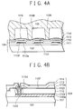
- FIG. 4A is a schematic sectional view of a main portion of another embodiment of the ink jet head, as seen from the same direction in FIG. 1A; and FIG. 4B is a schematic sectional view of the main portion shown in FIG. 4A, as seen from the same direction in FIG. 1B.
- This embodiment is different from the previous embodiment in that the electrodes under the upper insulating layer 1112 are formed not as a common conductive layer in a wide and flat shape, but as individually separated conductive layers for each heat generating portion 1102.
- Each of the electrodes has a multi-layer structure having an upper electrode layer 1110f and a lower electrode layer 1110e, and the upper electrode layer 1110f is formed of a high melting point metal.
- At least the uppermost layer (upper electrode layer 1110f) is made of a high melting point metal, and the high melting point metal layer functions to diffuse the heat and to lower the thermal effect and nevertheless the layer itself is not affected by the heat. Accordingly, it becomes possible to prevent or suppress the generation of a hillock and hence to prevent or suppress the generation of a projecting portion on the bubbling surface.
- the lower electrodes are independently disposed, the heat generated by each heat generating portion 1102 is prevented from being transmitted to the adjacent heat generating portion by way of the lower electrode. An energy loss due to the thermal diffusion through the lower electrodes can be also suppressed.
- the substrate for an ink jet head in this embodiment is manufactured by changing the pattern used in the previous embodiment in such a manner that the material layers of the electrode layers are separately and independently patterned.
- FIG. 5A is a schematic perspective view showing one embodiment of an ink jet head according to the present invention.
- FIG. 5B is a schematic sectional view taken along line C-C' of the ink jet head shown in FIG. 5A.
- the main portion of the schematic sectional view taken along line D-D' of the ink jet head shown in FIG. 5A is equivalent to that shown in FIG. 1A.
- An ink jet head 12 is so constructed that a resin-made top plate 105 is pressingly joined to a substrate 104 for an ink jet head by using an elastic member such as a spring.
- the top plate 105 includes a discharge opening plate 1104 provided with discharge openings 1101, and a path wall member 1109 integrated with the discharge opening plate 1104.
- a common ink chamber 1106 is provided in the top plate 105. Ink is supplied from an ink tank for reserving ink to the common ink chamber 1106 by way of a supply opening 107. The ink supplied to the common ink chamber 1106 is introduced into each ink path 1108, and is held in the state that meniscus is formed at the discharge opening 1101.
- the electrothermal converting body When the electrothermal converting body is driven for generating heat, a change in the state including the film-boiling of ink occurs in ink, to thus form a bubble. On the basis of the growth of the bubbles, the ink is discharged from the discharge opening 1101.
- FIG. 6 is a schematic perspective view showing a main portion of an ink jet apparatus 15 on which an ink jet pen in a cartridge form assembled with the ink jet head shown in FIGs. 5A and 5B is mounted.
- a lead screw 256 is rotated. Since a pin (not shown) engaged with a screw groove 255 of the lead screw 256 is provided on a carriage 16, the carriage 16 is reciprocated in the directions shown by the arrows "a" and "b" along with the rotation of the lead screw 256.
- Reference numeral 253 indicates a paper pressing plate, which presses a paper sheet 272 against a platen 251 in the moving direction of the carriage 16.
- Reference numeral 258 and 259 indicate a photo-coupler which acts as a home position detecting means for confirming the presence of a lever 257 of the carriage 16 in this range and switching the rotational direction of the motor 264.
- Reference numeral 11 indicates an ink jet pen of a cartridge type integrally provided with an ink tank.
- Reference numeral 265 indicates a cap for capping the ink discharge opening of the ink jet pen. The cap 265 is supported by a supporting member 270.
- Reference numeral 273 indicates a suction means for performing the suction from the ink discharge opening by way of the cap 265 and for sucking and recovering the head by way of an opening 271 of the cap 265.
- Reference numeral 266 indicates a blade for cleaning the surface on which the ink discharge opening is provided.
- Reference numeral 268 indicates a member for moving the blade 266 in the longitudinal direction. These are supported on the main body supporting plate 267.
- FIGs. 1A, 1B and 1C A plurality of substrates for ink jet heads shown in FIGs. 1A, 1B and 1C were fabricated in the following procedure.
- a 1.5 ⁇ m thick lower insulating layer 1111 made of silicon oxide was formed on a base member 103 made of single crystal silicon by thermal oxidation.
- a 5,500 ⁇ thick Al layer and a 2,000 ⁇ thick Ta layer were sequentially formed by continuous sputtering.
- the Ta layer was formed so as to be applied with a compressive stress of 5 ⁇ 109 dyn/cm2 by adjusting argon pressure upon sputtering at 1.8 Pa.
- the Al layer and Ta layer were simultaneously patterned by dry-etching using a mixed gas of BCl3(46%), Cl2(36%) and N2(18%), thus forming a lower electrode layer 1110b made of Al and an upper electrode layer 1110c made of Ta formed thereon shown in FIGs. 1B and 1C.
- a 1.4 ⁇ m thick upper insulating layer 1112 made of silicon oxide was formed by plasma CVD, and then etched using ammonium fluoride, to form contact through-holes 1105.
- a 600 ⁇ thick tantalum nitride layer was formed by sputtering, and patterned by etching, thus forming a resistor layer 1103 having a shape shown in FIG. 1.
- a 5,500 ⁇ thick pure Al layer was formed by sputtering, and patterned by etching, thus forming individual electrodes 1110a and connection electrodes 1110d shown in FIG. 1A.
- a 1.0 ⁇ m thick lower protective layer made of silicon oxide was formed by plasma CVD.
- a 2,300 ⁇ thick upper protective layer 1114 made of Ta was formed by sputtering.
- a top plate 105 made of polysulfone was pressingly joined to each of a plurality of the substrates 10 for ink jet heads thus manufactured by using a spring (not shown).
- a plurality of the ink jet heads 12 shown in FIGs. 5A and 5B were obtained.
- the arrangement density of the discharge openings 1101 was set at 16 nozzles/mm, and the number of the discharge openings 1101 was set at 128 nozzles.
- a plurality of substrates for ink jet heads shown in FIGs. 1A, 1B and 1C were manufactured in the same manner as in Example 1, except that the material of the upper electrode layer was changed from Ta to W. Namely, a 5,500 ⁇ thick Al layer and a 2,000 ⁇ thick W layer were sequentially formed by continuous sputtering. In this case, the W layer was formed so as to be applied with a compressive stress of 5 ⁇ 109 dyn/cm2 by adjusting argon pressure upon sputtering at the same value as that of Example 1. The Al layer and W layer were simultaneously patterned by dry-etching in the same manner as in Example 1, thus forming a lower electrode layer 1110b made of Al and an upper electrode layer 1110c made of W formed thereon shown in FIGs. 1B and 1C.
- a top plate 105 made of polysulfone was pressingly joined to each of a plurality of the substrates 10 for ink jet heads thus manufactured using a spring (not shown).
- a plurality of the ink jet heads 12 shown in FIGs. 5A and 5B were obtained.
- the arrangement density of the discharge openings 1101 was set at 16 nozzles/mm, and the number of the discharge openings 1101 was set at 128 nozzles.
- a plurality of substrates for ink jet heads shown in FIGs. 1A, 1B and 1C were manufactured in the same manner as in Example 1, except that the material of the upper electrode layer was changed from Ta to Cr. Namely, a 5,500 ⁇ thick Al layer and a 2,000 ⁇ thick Cr layer were sequentially formed by continuous sputtering. In this case, the Cr layer was formed so as to be applied with a compressive stress of 5 ⁇ 109 dyn/cm2 by adjusting argon pressure upon sputtering at the same value as that of Example 1. The Al layer and Cr layer were simultaneously patterned by dry-etching in the same manner as in Example 1, thus forming a lower electrode layer 1110b made of Al and an upper electrode layer 1110c made of Cr formed thereon shown in FIGs. 1B and 1C.
- a top plate 105 made of polysulfone was pressingly joined to each of a plurality of the substrates 10 for ink jet heads thus manufactured using a spring (not shown).
- a plurality of the ink jet heads 12 shown in FIGs. 5A and 5B were obtained.
- the arrangement density of the discharge openings 1101 was set at 16 nozzles/mm, and the number of the discharge openings 1101 was set at 128 nozzles.
- a plurality of substrates for ink jet heads shown in FIGs. 1A, 1B and 1C were manufactured in the same manner as in Example 1, except that the material of the upper electrode layer was changed from Ta to Ti. Namely, a 5,500 ⁇ thick Al layer and a 2,000 ⁇ thick Ti layer were sequentially formed by continuous sputtering. In this case, the Ti layer was formed so as to be applied with a compressive stress of 5 ⁇ 109 dyn/cm2 by adjusting argon pressure upon sputtering at the same value as that of Example 1. The Al layer and Ti layer were simultaneously patterned by dry-etching in the same manner as in Example 1, thus forming a lower electrode layer 1110b made of Al and an upper electrode layer 1110c made of Ti formed thereon shown in FIGs. 1B and 1C.
- a top plate 105 made of polysulfone was pressingly joined to each of a plurality of the substrates 10 for ink jet heads thus manufactured using a spring (not shown).
- a plurality of the ink jet heads 12 shown in FIGs. 5A and 5B were obtained.
- the arrangement density of the discharge openings 1101 was set at 16 nozzles/mm, and the number of the discharge openings 1101 was set at 128 nozzles.
- a plurality of substrates for ink jet heads shown in FIGs. 1A, 1B and 1C were manufactured in the same manner as in Example 1, except that the material of the upper electrode layer was changed from Ta to Mo. Namely, a 5,500 ⁇ thick Al layer and a 2,000 ⁇ thick Mo layer were sequentially formed by continuous sputtering. In this case, the Mo layer was formed so as to be applied with a compressive stress of 5 ⁇ 109 dyn/cm2 by adjusting argon pressure upon sputtering at the same value as that of Example 1. The Al layer and Mo layer were simultaneously patterned by dry-etching in the same manner as in Example 1, thus forming a lower electrode layer 1110b made of Al and an upper electrode layer 1110c made of Mo formed thereon shown in FIGs. 1B and 1C.
- a top plate 105 made of polysulfone was pressingly joined to each of a plurality of the substrates 10 for ink jet heads thus manufactured using a spring (not shown).
- a plurality of the ink jet heads 12 shown in FIGs. 5A and 5B were obtained.
- the arrangement density of the discharge openings 1101 was set at 16 nozzles/mm, and the number of the discharge openings 1101 was set at 128 nozzles.
- a plurality of substrates for ink jet heads shown in FIGs. 1A, 1B and 1C were manufactured in the same manner as in Example 1, except that the material of the upper electrode layer was changed from Ta to Ti-Mo alloy. Namely, a 5,500 ⁇ thick Al layer and a 2,000 ⁇ thick Ti-Mo alloy (Mo: 5%, the balance: Ti) layer were sequentially formed by continuous sputtering. In this case, the Ti-Mo alloy layer was formed so as to be applied with a compressive stress of 5 ⁇ 109 dyn/cm2 by adjusting argon pressure upon sputtering at the same value as that of Example 1.
- the Al layer and Ti-Mo alloy layer were simultaneously patterned by dry-etching in the same manner as in Example 1, thus forming a lower electrode layer 1110b made of Al and an upper electrode layer 1110c made of Ti-Mo alloy formed thereon shown in FIGs. 1B and 1C.
- a top plate 105 made of polysulfone was pressingly joined to each of a plurality of the substrates 10 for ink jet heads thus manufactured using a spring (not shown).
- a plurality of the ink jet heads 12 shown in FIGs. 5A and 5B were obtained.
- the arrangement density of the discharge openings 1101 was set at 16 nozzles/mm, and the number of the discharge openings 1101 was set at 128 nozzles.
- a plurality of substrates for ink jet heads shown in FIGs. 1A, 1B and 1C were manufactured in the same manner as in Example 1, except that the material of the upper electrode layer was changed from Ta to Ti-Cr alloy. Namely, a 5,500 ⁇ thick Al layer and a 2,000 ⁇ thick Ti-Cr alloy (Cr: 5%, the balance: Ti) layer were sequentially formed by continuous sputtering. In this case, the Ti-Cr alloy layer was formed so as to be applied with a compressive stress of 5 ⁇ 109 dyn/cm2 by adjusting argon pressure upon sputtering at the same value as that of Example 1.
- the Al layer and Ti-Cr alloy layer were simultaneously patterned by dry-etching in the same manner as in Example 1, thus forming a lower electrode layer 1110b made of Al and an upper electrode layer 1110c made of Ti-Cr alloy formed thereon shown in FIGs. 1B and 1C.
- a top plate 105 made of polysulfone was pressingly joined to each of a plurality of the substrates 10 for ink jet heads thus manufactured using a spring (not shown).
- a plurality of the ink jet heads 12 shown in FIGs. 5A and 5B were obtained.
- the arrangement density of the discharge openings 1101 was set at 16 nozzles/mm, and the number of the discharge openings 1101 was set at 128 nozzles.
- a plurality of substrates for ink jet heads shown in FIGs. 1A, 1B and 1C were manufactured in the same manner as in Example 1, except that the material of the upper electrode layer was changed from Ta to Ti-Al alloy. Namely, a 5,500 ⁇ thick Al layer and a 2,000 ⁇ thick Ti-Al alloy (Al : 5%, the balance: Ti) layer were sequentially formed by continuous sputtering. In this case, the Ti-Al alloy layer was formed so as to be applied with a compressive stress of 5 ⁇ 109 dyn/cm2 by adjusting argon pressure upon sputtering at the same value as that of Example 1.
- the Al layer and Ti-Al alloy layer were simultaneously patterned by dry-etching in the same manner as in Example 1, thus forming a lower electrode layer 1110b made of Al and an upper electrode layer 1110c made of Ti-Al alloy formed thereon shown in FIGs. 1B and 1C.
- a top plate 105 made of polysulfone was pressingly joined to each of a plurality of the substrates 10 for ink jet heads thus manufactured using a spring (not shown).
- a plurality of the ink jet heads 12 shown in FIGs. 5A and 5B were obtained.
- the arrangement density of the discharge openings 1101 was set at 16 nozzles/mm, and the number of the discharge openings 1101 was set at 128 nozzles.
- a plurality of substrates for ink jet heads shown in FIGs. 1A, 1B and 1C were manufactured in the same manner as in Example 1, except that the material of the lower electrode layer was changed from Al to Cu. Namely, a 5,500 ⁇ thick Cu layer and a 2,000 ⁇ thick Ta layer were sequentially formed by continuous sputtering. In this case, the Ta layer was formed so as to be applied with a compressive stress of 5 ⁇ 109 dyn/cm2 by adjusting argon pressure upon sputtering at the same value as that of Example 1. The Cu layer and Ta layer were simultaneously patterned by dry-etching in the same manner as in Example 1, thus forming a lower electrode layer 1110b made of Cu and an upper electrode layer 1110c made of Ta formed thereon shown in FIGs. 1B and 1C.
- a top plate 105 made of polysulfone was pressingly joined to each of a plurality of the substrates 10 for ink jet heads thus manufactured using a spring (not shown).
- a plurality of the ink jet heads 12 shown in FIGs. 5A and 5B were obtained.
- the arrangement density of the discharge openings 1101 was set at 16 nozzles/mm, and the number of the discharge openings 1101 was set at 128 nozzles.
- a plurality of substrates for ink jet heads shown in FIGs. 1A, 1B and 1C were manufactured in the same manner as in Example 1, except that the material of the lower electrode layer was changed from Al to Al-Si alloy. Namely, a 5,500 ⁇ thick Al-Si alloy (Si: 10%, the balance: Al) layer and a 2,000 ⁇ thick Ta layer were sequentially formed by continuous sputtering. In this case, the Ta layer was formed so as to be applied with a compressive stress of 5 ⁇ 109 dyn/cm2 by adjusting argon pressure upon sputtering at the same value as that of Example 1.
- the Al-Si alloy layer and Ta layer were simultaneously patterned by dry-etching in the same manner as in Example 1, thus forming a lower electrode layer 1110b made of Al-Si alloy and an upper electrode layer 1110c made of Ta formed thereon shown in FIGs. 1B and 1C.
- a top plate 105 made of polysulfone was pressingly joined to each of a plurality of the substrates 10 for ink jet heads thus manufactured using a spring (not shown).
- a plurality of the ink jet heads 12 shown in FIGs. 5A and 5B were obtained.
- the arrangement density of the discharge openings 1101 was set at 16 nozzles/mm, and the number of the discharge openings 1101 was set at 128 nozzles.
- a plurality of substrates for ink jet heads shown in FIGs. 1A, 1B and 1C were manufactured in the same manner as in Example 1, except that the material of the lower electrode layer was changed from Al to Al-Cu alloy. Namely, a 5,500 ⁇ thick Al-Cu alloy (Cu: 10%, the balance: Al) layer and a 2,000 ⁇ thick Ta layer were sequentially formed by continuous sputtering. In this case, the Ta layer was formed so as to be applied with a compressive stress of 5 ⁇ 109 dyn/cm2 by adjusting argon pressure upon sputtering at the same value as that of Example 1.
- the Al-Cu alloy layer and Ta layer were simultaneously patterned by dry-etching in the same manner as in Example 1, thus forming a lower electrode layer 1110b made of Al-Cu alloy and an upper electrode layer 1110c made of Ta formed thereon shown in FIGs. 1B and 1C.
- a top plate 105 made of polysulfone was pressingly joined to each of a plurality of the substrates 10 for ink jet heads thus manufactured using a spring (not shown).
- a plurality of the ink jet heads 12 shown in FIGs. 5A and 5B were obtained.
- the arrangement density of the discharge openings 1101 was set at 16 nozzles/mm, and the number of the discharge openings 1101 was set at 128 nozzles.
- a plurality of substrates for ink jet heads shown in FIGs. 4A and 4B were manufactured in the same manner as in Example 1, except that the process of patterning the lower electrode material layer and upper electrode material layer by etching was changed as follows. Namely, different from Example 1, the Al layer and Ta layer were patterned by dry-etching on the basis of such a pattern that the lower electrode layers 1110e made of Al and the upper electrode layers 1110f made of Ta were separately and independently formed as shown in FIGs. 4A and 4B.
- a top plate 105 made of polysulfone was pressingly joined to each of a plurality of the substrates 10 for ink jet head according to the embodiment thus manufactured using a spring (not shown).
- a plurality of the ink jet heads 12 according to the embodiment shown in FIGs. 5A and 5B were obtained.
- the density in arrangement of the discharge openings 1101 of the ink jet head 12 was set at 16 nozzles/mm, and the number of the discharge openings 1101 was 128 nozzles.
- a plurality of substrates for ink jet heads shown in FIGs. 4A and 4B were manufactured in the same manner as in Example 2, except that the process of patterning the lower electrode material layer and upper electrode material layer by etching was changed as follows. Namely, different from Example 2, the Al layer and W layer were patterned by dry-etching on the basis of such a pattern that the lower electrode layers 1110e made of Al and the upper electrode layers 1110f made of W were separately and independently formed as shown in FIGs. 4A and 4B.
- a top plate 105 made of polysulfone was pressingly joined to each of a plurality of the substrates 10 for ink jet head according to the embodiment thus manufactured using a spring (not shown).
- a plurality of the ink jet heads 12 according to the embodiment shown in FIGs. 5A and 5B were obtained.
- the density in arrangement of the discharge openings 1101 of the ink jet head 12 was set at 16 nozzles/mm, and the number of the discharge openings 1101 was 128 nozzles.
- a plurality of substrates for ink jet heads shown in FIGs. 4A and 4B were manufactured in the same manner as in Example 3, except that the process of patterning the lower electrode material layer and upper electrode material layer by etching was changed as follows. Namely, different from Example 3, the Al layer and Cr layer were patterned by dry-etching on the basis of such a pattern that the lower electrode layers 1110e made of Al and the upper electrode layers 1110f made of Cr were separately and independently formed as shown in FIGs. 4A and 4B.
- a top plate 105 made of polysulfone was pressingly joined to each of a plurality of the substrates 10 for ink jet head according to the embodiment thus manufactured using a spring (not shown).
- a plurality of the ink jet heads 12 according to the embodiment shown in FIGs. 5A and 5B were obtained.
- the density in arrangement of the discharge openings 1101 of the ink jet head 12 was set at 16 nozzles/mm, and the number of the discharge openings 1101 was 128 nozzles.
- a plurality of substrates for ink jet heads shown in FIGs. 4A and 4B were manufactured in the same manner as in Example 4, except that the process of patterning the lower electrode material layer and upper electrode material layer by etching was changed as follows. Namely, different from Example 4, the Al layer and Ti layer were patterned by dry-etching on the basis of such a pattern that the lower electrode layers 1110e made of Al and the upper electrode layers 1110f made of Ti were separately and independently formed as shown in FIGs. 4A and 4B.
- a top plate 105 made of polysulfone was pressingly joined to each of a plurality of the substrates 10 for ink jet head according to the embodiment thus manufactured using a spring (not shown).
- a plurality of the ink jet heads 12 according to the embodiment shown in FIGs. 5A and 5B were obtained.
- the density in arrangement of the discharge openings 1101 of the ink jet head 12 was set at 16 nozzles/mm, and the number of the discharge openings 1101 was 128 nozzles.
- a plurality of substrates for ink jet heads shown in FIGs. 4A and 4B were manufactured in the same manner as in Example 5, except that the process of patterning the lower electrode material layer and upper electrode material layer by etching was changed as follows. Namely, different from Example 5, the Al layer and Mo layer were patterned by dry-etching on the basis of such a pattern that the lower electrode layers 1110e made of Al and the upper electrode layers 1110f made of Mo were separately and independently formed as shown in FIGs. 4A and 4B.
- a top plate 105 made of polysulfone was pressingly joined to each of a plurality of the substrates 10 for ink jet head according to the embodiment thus manufactured using a spring (not shown).
- a plurality of the ink jet heads 12 according to the embodiment shown in FIGs. 5A and 5B were obtained.
- the density in arrangement of the discharge openings 1101 of the ink jet head 12 was set at 16 nozzles/mm, and the number of the discharge openings 1101 was 128 nozzles.
- a plurality of substrates for ink jet heads shown in FIGs. 4A and 4B were manufactured in the same manner as in Example 6, except that the process of patterning the lower electrode material layer and upper electrode material layer by etching was changed as follows. Namely, different from Example 6, the Al layer and Ti-Mo alloy layer were patterned by dry-etching on the basis of such a pattern that the lower electrode layers 1110e made of Al and the upper electrode layers 1110f made of Ti-Mo alloy were separately and independently formed as shown in FIGs. 4A and 4B.
- a top plate 105 made of polysulfone was pressingly joined to each of a plurality of the substrates 10 for ink jet head according to the embodiment thus manufactured using a spring (not shown).
- a plurality of the ink jet heads 12 according to the embodiment shown in FIGs. 5A and 5B were obtained.
- the density in arrangement of the discharge openings 1101 of the ink jet head 12 was set at 16 nozzles/mm, and the number of the discharge openings 1101 was 128 nozzles.
- a plurality of substrates for ink jet heads shown in FIGs. 4A and 4B were manufactured in the same manner as in Example 7, except that the process of patterning the lower electrode material layer and upper electrode material layer by etching was changed as follows. Namely, different from Example 7, the Al layer and Ti-Cr alloy layer were patterned by dry-etching on the basis of such a pattern that the lower electrode layers 1110e made of Al and the upper electrode layers 1110f made of Ti-Cr alloy were separately and independently formed as shown in FIGs. 4A and 4B.
- a top plate 105 made of polysulfone was pressingly joined to each of a plurality of the substrates 10 for ink jet head according to the embodiment thus manufactured using a spring (not shown).
- a plurality of the ink jet heads 12 according to the embodiment shown in FIGs. 5A and 5B were obtained.
- the density in arrangement of the discharge openings 1101 of the ink jet head 12 was set at 16 nozzles/mm, and the number of the discharge openings 1101 was 128 nozzles.
- a plurality of substrates for ink jet heads shown in FIGs. 4A and 4B were manufactured in the same manner as in Example 8, except that the process of patterning the lower electrode material layer and upper electrode material layer by etching was changed as follows. Namely, different from Example 8, the Al layer and Ti-Al alloy layer were patterned by dry-etching on the basis of such a pattern that the lower electrode layers 1110e made of Al and the upper electrode layers 1110f made of Ti-Al alloy were separately and independently formed as shown in FIGs. 4A and 4B.
- a top plate 105 made of polysulfone was pressingly joined to each of a plurality of the substrates 10 for ink jet head according to the embodiment thus manufactured using a spring (not shown).
- a plurality of the ink jet heads 12 according to the embodiment shown in FIGs. 5A and 5B were obtained.
- the density in arrangement of the discharge openings 1101 of the ink jet head 12 was set at 16 nozzles/mm, and the number of the discharge openings 1101 was 128 nozzles.
- a plurality of substrates for ink jet heads shown in FIGs. 4A and 4B were manufactured in the same manner as in Example 9, except that the process of patterning the lower electrode material layer and upper electrode material layer by etching was changed as follows. Namely, different from Example 9, the Cu layer and Ta alloy layer were patterned by dry-etching on the basis of such a pattern that the lower electrode layers 1110e made of Cu and the upper electrode layers 1110f made of Ta alloy were separately and independently formed as shown in FIGs. 4A and 4B.
- a top plate 105 made of polysulfone was pressingly joined to each of a plurality of the substrates 10 for ink jet head according to the embodiment thus manufactured using a spring (not shown).
- a plurality of the ink jet heads 12 according to the embodiment shown in FIGs. 5A and 5B were obtained.
- the density in arrangement of the discharge openings 1101 of the ink jet head 12 was set at 16 nozzles/mm, and the number of the discharge openings 1101 was 128 nozzles.
- a plurality of substrates for ink jet heads shown in FIGs. 4A and 4B were manufactured in the same manner as in Example 10, except that the process of patterning the lower electrode material layer and upper electrode material layer by etching was changed as follows. Namely, different from Example 10, the Al-Si alloy layer and Ta alloy layer were patterned by dry-etching on the basis of such a pattern that the lower electrode layers 1110e made of Al-Si alloy and the upper electrode layers 1110f made of Ta alloy were separately and independently formed as shown in FIGs. 4A and 4B.
- a top plate 105 made of polysulfone was pressingly joined to each of a plurality of the substrates 10 for ink jet head according to the embodiment thus manufactured using a spring (not shown).
- a plurality of the ink jet heads 12 according to the embodiment shown in FIGs. 5A and 5B were obtained.
- the density in arrangement of the discharge openings 1101 of the ink jet head 12 was set at 16 nozzles/mm, and the number of the discharge openings 1101 was 128 nozzles.
- a plurality of substrates for ink jet heads shown in FIGs. 4A and 4B were manufactured in the same manner as in Example 11, except that the process of patterning the lower electrode material layer and upper electrode material layer by etching was changed as follows. Namely, different from Example 11, the Al-Cu alloy layer and Ta alloy layer were patterned by dry-etching on the basis of such a pattern that the lower electrode layers 1110e made of Al-Cu alloy and the upper electrode layers 1110f made of Ta alloy were separately and independently formed as shown in FIGs. 4A and 4B.
- a top plate 105 made of polysulfone was pressingly joined to each of a plurality of the substrates 10 for ink jet head according to the embodiment thus manufactured using a spring (not shown).
- a plurality of the ink jet heads 12 according to the embodiment shown in FIGs. 5A and 5B were obtained.
- the density in arrangement of the discharge openings 1101 of the ink jet head 12 was set at 16 nozzles/mm, and the number of the discharge openings 1101 was 128 nozzles.
- a plurality of substrates for ink jet heads shown in FIGs. 2A and 2B were manufactured in the same manner as in Example 1, except that the process of forming the lower electrode layer and upper electrode layer was changed as follows. Namely, a 7,500 ⁇ thick pure Al layer was formed by sputtering, and patterned by dry-etching using the same gas as that in Example 1, thus forming an electrode layer 1110g having a single layer structure of Al.
- a top plate 105 made of polysulfone was pressingly joined to each of a plurality of the substrates 10 for ink jet head according to the embodiment thus manufactured using a spring (not shown).
- a plurality of the ink jet heads 12 according to the embodiment shown in FIGs. 5A and 5B were obtained.
- the density in arrangement of the discharge openings 1101 of the ink jet head 12 was set at 16 nozzles/mm, and the number of the discharge openings 1101 was 128 nozzles.
- Example 1 Each of the ink jet heads 12 obtained in Example 1 and Comparative Example was assembled in the ink jet pen 11, and the ink jet pen 11 was mounted on the ink jet apparatus shown in FIG. 6.
- the discharge endurance test for each ink jet head was made by performing ink discharge using the above ink jet apparatus 15.
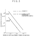
- FIG. 3 is a graph for comparing the ink jet head of Example 1 with that of Comparative Example (Background Art) in the discharge endurance performance.
- the ordinate indicates the discharging pulse number
- the abscissa indicates the input energy amount in driving voltage (Vop)/bubble forming voltage (Vth).
- the graph shows the number of the discharging pulse indicated along the ordinate at the time when either of the heat generators is broken in accordance with an input energy amount indicated along the abscissa.
- 10 pieces of ink jet heads were tested, and the average value thereof was plotted in the graph shown in FIG. 3. In this test, the width of the discharging pulse was 5 ⁇ s.
- the ink jet head in Example 1 exhibits an excellent durability which is about four times that of the ink jet head in Comparative Example.
- Example 1 and Comparative Example were disassembled for the same discharging pulse number, and the state of the bubbling surface was observed. As a result, it was confirmed that in the ink jet head in Example 1, the presence of projecting portions was little observed on the bubbling surface, as compared with the ink jet head in Comparative Example.
- a substrate for an ink jet head comprises a base member and an electrothermal converting body formed on the base member, the electrothermal converting body including a resistor layer and a pair of electrode layers connected to the resistor layer wherein the resistor layer positioned between a pair of the electrode layers serves as a heat generating portion for generating thermal energy utilized for discharging ink; wherein one of a pair of the electrode layers passes under the heat generating portion; an electrode layer positioned under the heat generating portion has a multi-layer structure composed of a plurality of layers; and at least one of a plurality of the layers, being nearest to the heat generating portion, is made of a metal having a melting point of 1500°C or more at 1 atm.
- An ink jet head using this substrate is able to prolong service life while reducing a failure ratio, and to continue preferable ink discharge for a long period of time.
Landscapes
- Engineering & Computer Science (AREA)
- Manufacturing & Machinery (AREA)
- Particle Formation And Scattering Control In Inkjet Printers (AREA)
Applications Claiming Priority (3)
| Application Number | Priority Date | Filing Date | Title |
|---|---|---|---|
| JP58534/94 | 1994-03-29 | ||
| JP5853494 | 1994-03-29 | ||
| JP5853494 | 1994-03-29 |
Publications (3)
| Publication Number | Publication Date |
|---|---|
| EP0674995A2 true EP0674995A2 (de) | 1995-10-04 |
| EP0674995A3 EP0674995A3 (de) | 1997-01-15 |
| EP0674995B1 EP0674995B1 (de) | 2002-03-06 |
Family
ID=13087110
Family Applications (1)
| Application Number | Title | Priority Date | Filing Date |
|---|---|---|---|
| EP95104550A Expired - Lifetime EP0674995B1 (de) | 1994-03-29 | 1995-03-28 | Substrat für Tintenstrahlkopf, Tintenstrahlkopf, Tintenstrahlschreiber und Tintenstrahlgerät |
Country Status (5)
| Country | Link |
|---|---|
| US (1) | US6056391A (de) |
| EP (1) | EP0674995B1 (de) |
| KR (1) | KR0156612B1 (de) |
| CN (1) | CN1096951C (de) |
| DE (1) | DE69525669T2 (de) |
Cited By (14)
| Publication number | Priority date | Publication date | Assignee | Title |
|---|---|---|---|---|
| EP0924079A2 (de) * | 1997-12-18 | 1999-06-23 | Canon Kabushiki Kaisha | Substrat zur Verwendung in einem Tintenstrahlaufzeichungskopf, Verfahren zur Herstellung dieses Substrats, Tintenstrahlaufzeichnungskopf und Tintenstrahlaufzeichnungsgerät |
| EP0890438A3 (de) * | 1997-07-03 | 1999-11-10 | Lexmark International, Inc. | Druckkopf mit Heizelement mit Leitern in räumlich verschobenen Ebenen |
| EP0899108A3 (de) * | 1997-07-03 | 1999-11-10 | Lexmark International, Inc. | Tintenstrahldruckkopf und Chip mit einem Heizelement |
| EP0921004A3 (de) * | 1997-12-05 | 2000-04-26 | Canon Kabushiki Kaisha | Flüssigkeitsausstosskopf , Aufzeichnungsgerät und Flüssigkeitsausstosskopfenherstellungsverfahren |
| EP1000745A3 (de) * | 1998-10-27 | 2001-01-24 | Canon Kabushiki Kaisha | Platine zur elektrothermischen Umwandlung, Tintenstrahldruckkopf und Tintenstrahlaufzeichnungsgerät mit derselben, und Verfahren zur Herstellung eines Tintenstrahldruckkopfes |
| EP1170129A2 (de) * | 2000-07-07 | 2002-01-09 | Hewlett-Packard Company | Tintenstrahldrucker und dazugehöriges Herstellungsverfahren |
| EP1216836A1 (de) * | 2000-12-20 | 2002-06-26 | Hewlett-Packard Company | Flüssigkeitsstrahldruckkopf und Verfahren für dessen Herstellung |
| US6457815B1 (en) | 2001-01-29 | 2002-10-01 | Hewlett-Packard Company | Fluid-jet printhead and method of fabricating a fluid-jet printhead |
| US6485132B1 (en) | 1997-12-05 | 2002-11-26 | Canon Kabushiki Kaisha | Liquid discharge head, recording apparatus, and method for manufacturing liquid discharge heads |
| US6513913B2 (en) | 2001-04-30 | 2003-02-04 | Hewlett-Packard Company | Heating element of a printhead having conductive layer between resistive layers |
| US6688729B1 (en) * | 1999-06-04 | 2004-02-10 | Canon Kabushiki Kaisha | Liquid discharge head substrate, liquid discharge head, liquid discharge apparatus having these elements, manufacturing method of liquid discharge head, and driving method of the same |
| EP1627743A1 (de) * | 2004-08-16 | 2006-02-22 | Canon Kabushiki Kaisha | Schaltungsplatte für Tintenstrahldruckkopf, Verfahren zu ihrer Herstellung, und damit ausgestattetem Tintenstrahldruckkopf |
| EP1627744A1 (de) * | 2004-08-16 | 2006-02-22 | Canon Kabushiki Kaisha | Schaltungsplatte für Tintenstrahldruckkopf, Verfahren zu ihrer Herstellung, und damit ausgestattetem Tintenstrahldruckkopf |
| EP1627741A1 (de) * | 2004-08-16 | 2006-02-22 | Canon Kabushiki Kaisha | Schaltungsplatte für Tintenstrahldruckkopf, Verfahren zu ihrer Herstellung und damit ausgestatteter Tintenstrahldruckkopf |
Families Citing this family (8)
| Publication number | Priority date | Publication date | Assignee | Title |
|---|---|---|---|---|
| US6331055B1 (en) * | 1999-08-30 | 2001-12-18 | Hewlett-Packard Company | Inkjet printhead with top plate bubble management |
| US6853076B2 (en) | 2001-09-21 | 2005-02-08 | Intel Corporation | Copper-containing C4 ball-limiting metallurgy stack for enhanced reliability of packaged structures and method of making same |
| US7083265B2 (en) | 2001-10-31 | 2006-08-01 | Hewlett-Packard Development Company, L.P. | Circuit routing for printhead having increased corrosion resistance |
| JP4393303B2 (ja) * | 2003-09-05 | 2010-01-06 | キヤノン株式会社 | 半導体装置の製造方法 |
| US7240997B2 (en) | 2004-02-25 | 2007-07-10 | Hewlett-Packard Development Company, L.P. | Fluid ejection device metal layer layouts |
| JP4182035B2 (ja) * | 2004-08-16 | 2008-11-19 | キヤノン株式会社 | インクジェットヘッド用基板、該基板の製造方法および前記基板を用いるインクジェットヘッド |
| JP4290154B2 (ja) * | 2004-12-08 | 2009-07-01 | キヤノン株式会社 | 液体吐出記録ヘッドおよびインクジェット記録装置 |
| CN103862870B (zh) * | 2014-03-27 | 2016-06-15 | 苏州锐发打印技术有限公司 | 延长喷墨头加热器寿命的方法及喷墨头加热器 |
Citations (5)
| Publication number | Priority date | Publication date | Assignee | Title |
|---|---|---|---|---|
| US4096510A (en) * | 1974-08-19 | 1978-06-20 | Matsushita Electric Industrial Co., Ltd. | Thermal printing head |
| US4458256A (en) * | 1979-03-06 | 1984-07-03 | Canon Kabushiki Kaisha | Ink jet recording apparatus |
| JPS63297060A (ja) * | 1987-05-29 | 1988-12-05 | Matsushita Graphic Commun Syst Inc | 静電記録用記録電極 |
| JPH03234672A (ja) * | 1990-02-13 | 1991-10-18 | Alps Electric Co Ltd | サーマルヘッド |
| EP0585890A2 (de) * | 1992-09-01 | 1994-03-09 | Canon Kabushiki Kaisha | Farbstrahldruckkopf und zugehöriges Farbstrahlgerät |
Family Cites Families (6)
| Publication number | Priority date | Publication date | Assignee | Title |
|---|---|---|---|---|
| JP2611981B2 (ja) * | 1987-02-04 | 1997-05-21 | キヤノン株式会社 | インクジエツト記録ヘツド用基板及びインクジエツト記録ヘツド |
| JP2801196B2 (ja) * | 1987-11-20 | 1998-09-21 | キヤノン株式会社 | 液体噴射装置 |
| JP2718724B2 (ja) * | 1987-11-27 | 1998-02-25 | キヤノン株式会社 | インクジェット記録装置、該装置用キャップユニットおよびインクジェットヘッドの回復方法 |
| US5081474A (en) * | 1988-07-04 | 1992-01-14 | Canon Kabushiki Kaisha | Recording head having multi-layer matrix wiring |
| JP2840271B2 (ja) * | 1989-01-27 | 1998-12-24 | キヤノン株式会社 | 記録ヘッド |
| JPH0628272A (ja) * | 1992-07-10 | 1994-02-04 | Hitachi Ltd | 試験機能を備えた入出力装置 |
-
1995
- 1995-03-28 DE DE69525669T patent/DE69525669T2/de not_active Expired - Lifetime
- 1995-03-28 EP EP95104550A patent/EP0674995B1/de not_active Expired - Lifetime
- 1995-03-28 US US08/411,890 patent/US6056391A/en not_active Expired - Lifetime
- 1995-03-29 KR KR1019950006869A patent/KR0156612B1/ko not_active IP Right Cessation
- 1995-03-29 CN CN95103615A patent/CN1096951C/zh not_active Expired - Fee Related
Patent Citations (5)
| Publication number | Priority date | Publication date | Assignee | Title |
|---|---|---|---|---|
| US4096510A (en) * | 1974-08-19 | 1978-06-20 | Matsushita Electric Industrial Co., Ltd. | Thermal printing head |
| US4458256A (en) * | 1979-03-06 | 1984-07-03 | Canon Kabushiki Kaisha | Ink jet recording apparatus |
| JPS63297060A (ja) * | 1987-05-29 | 1988-12-05 | Matsushita Graphic Commun Syst Inc | 静電記録用記録電極 |
| JPH03234672A (ja) * | 1990-02-13 | 1991-10-18 | Alps Electric Co Ltd | サーマルヘッド |
| EP0585890A2 (de) * | 1992-09-01 | 1994-03-09 | Canon Kabushiki Kaisha | Farbstrahldruckkopf und zugehöriges Farbstrahlgerät |
Non-Patent Citations (2)
| Title |
|---|
| PATENT ABSTRACTS OF JAPAN vol. 013, no. 122 (M-807), 27 March 1989 & JP-A-63 297060 (MATSUSHITA GRAPHIC COMMUN SYST INC), 5 December 1988, * |
| PATENT ABSTRACTS OF JAPAN vol. 016, no. 016 (M-1200), 16 January 1992 & JP-A-03 234672 (ALPS ELECTRIC CO LTD), 18 October 1991, * |
Cited By (30)
| Publication number | Priority date | Publication date | Assignee | Title |
|---|---|---|---|---|
| EP0890438A3 (de) * | 1997-07-03 | 1999-11-10 | Lexmark International, Inc. | Druckkopf mit Heizelement mit Leitern in räumlich verschobenen Ebenen |
| EP0899108A3 (de) * | 1997-07-03 | 1999-11-10 | Lexmark International, Inc. | Tintenstrahldruckkopf und Chip mit einem Heizelement |
| EP0921004A3 (de) * | 1997-12-05 | 2000-04-26 | Canon Kabushiki Kaisha | Flüssigkeitsausstosskopf , Aufzeichnungsgerät und Flüssigkeitsausstosskopfenherstellungsverfahren |
| US6485132B1 (en) | 1997-12-05 | 2002-11-26 | Canon Kabushiki Kaisha | Liquid discharge head, recording apparatus, and method for manufacturing liquid discharge heads |
| EP0924079A3 (de) * | 1997-12-18 | 1999-12-08 | Canon Kabushiki Kaisha | Substrat zur Verwendung in einem Tintenstrahlaufzeichungskopf, Verfahren zur Herstellung dieses Substrats, Tintenstrahlaufzeichnungskopf und Tintenstrahlaufzeichnungsgerät |
| US6578951B2 (en) | 1997-12-18 | 2003-06-17 | Canon Kabushiki Kaisha | Substrate for use of an ink jet recording head, a method for manufacturing such substrate, an ink jet recording head, and an ink jet recording apparatus |
| EP0924079A2 (de) * | 1997-12-18 | 1999-06-23 | Canon Kabushiki Kaisha | Substrat zur Verwendung in einem Tintenstrahlaufzeichungskopf, Verfahren zur Herstellung dieses Substrats, Tintenstrahlaufzeichnungskopf und Tintenstrahlaufzeichnungsgerät |
| EP1000745A3 (de) * | 1998-10-27 | 2001-01-24 | Canon Kabushiki Kaisha | Platine zur elektrothermischen Umwandlung, Tintenstrahldruckkopf und Tintenstrahlaufzeichnungsgerät mit derselben, und Verfahren zur Herstellung eines Tintenstrahldruckkopfes |
| US6443563B1 (en) | 1998-10-27 | 2002-09-03 | Canon Kabushiki Kaisha | Electro-thermal conversion device board, ink-jet recording head provided with the electro-thermal conversion device board, ink-jet recording apparatus using the same, and production method of ink-jet recording head |
| US6945633B2 (en) | 1999-06-04 | 2005-09-20 | Canon Kabushiki Kaisha | Liquid discharge head substrate, liquid discharge head, liquid discharge apparatus having these elements, manufacturing method of liquid discharge head, and driving method of the same |
| US6688729B1 (en) * | 1999-06-04 | 2004-02-10 | Canon Kabushiki Kaisha | Liquid discharge head substrate, liquid discharge head, liquid discharge apparatus having these elements, manufacturing method of liquid discharge head, and driving method of the same |
| US6481831B1 (en) | 2000-07-07 | 2002-11-19 | Hewlett-Packard Company | Fluid ejection device and method of fabricating |
| EP1170129A3 (de) * | 2000-07-07 | 2002-01-30 | Hewlett-Packard Company | Tintenstrahldrucker und dazugehöriges Herstellungsverfahren |
| EP1170129A2 (de) * | 2000-07-07 | 2002-01-09 | Hewlett-Packard Company | Tintenstrahldrucker und dazugehöriges Herstellungsverfahren |
| US6457814B1 (en) | 2000-12-20 | 2002-10-01 | Hewlett-Packard Company | Fluid-jet printhead and method of fabricating a fluid-jet printhead |
| EP1216836A1 (de) * | 2000-12-20 | 2002-06-26 | Hewlett-Packard Company | Flüssigkeitsstrahldruckkopf und Verfahren für dessen Herstellung |
| US6785956B2 (en) | 2000-12-20 | 2004-09-07 | Hewlett-Packard Development Company, L.P. | Method of fabricating a fluid jet printhead |
| US6457815B1 (en) | 2001-01-29 | 2002-10-01 | Hewlett-Packard Company | Fluid-jet printhead and method of fabricating a fluid-jet printhead |
| US6558969B2 (en) | 2001-01-29 | 2003-05-06 | Hewlett-Packard Development Company | Fluid-jet printhead and method of fabricating a fluid-jet printhead |
| US6513913B2 (en) | 2001-04-30 | 2003-02-04 | Hewlett-Packard Company | Heating element of a printhead having conductive layer between resistive layers |
| US7168157B2 (en) | 2001-04-30 | 2007-01-30 | Hewlett-Packard Development Company, L.P. | Method of fabricating a printhead |
| US7716832B2 (en) | 2001-04-30 | 2010-05-18 | Hewlett-Packard Development Company, L.P. | Method of manufacturing a fluid ejection device |
| EP1627743A1 (de) * | 2004-08-16 | 2006-02-22 | Canon Kabushiki Kaisha | Schaltungsplatte für Tintenstrahldruckkopf, Verfahren zu ihrer Herstellung, und damit ausgestattetem Tintenstrahldruckkopf |
| EP1627744A1 (de) * | 2004-08-16 | 2006-02-22 | Canon Kabushiki Kaisha | Schaltungsplatte für Tintenstrahldruckkopf, Verfahren zu ihrer Herstellung, und damit ausgestattetem Tintenstrahldruckkopf |
| EP1627741A1 (de) * | 2004-08-16 | 2006-02-22 | Canon Kabushiki Kaisha | Schaltungsplatte für Tintenstrahldruckkopf, Verfahren zu ihrer Herstellung und damit ausgestatteter Tintenstrahldruckkopf |
| US7374275B2 (en) | 2004-08-16 | 2008-05-20 | Canon Kabushiki Kaisha | Ink jet head circuit board with heaters and electrodes constructed to reduce corrosion, method of manufacturing the same and ink jet head using the same |
| US7681993B2 (en) | 2004-08-16 | 2010-03-23 | Canon Kabushiki Kaisha | Circuit board for ink jet head, method of manufacturing the same, and ink jet head using the same |
| CN1736716B (zh) * | 2004-08-16 | 2010-05-05 | 佳能株式会社 | 喷墨头用基板、该基板的制造方法和使用上述基板的喷墨头 |
| US7862155B2 (en) | 2004-08-16 | 2011-01-04 | Canon Kabushiki Kaisha | Ink jet head circuit board, method of manufacturing the same and ink jet head using the same |
| US7954238B2 (en) | 2004-08-16 | 2011-06-07 | Canon Kabushiki Kaisha | Method of manufacturing ink jet circuit board with heaters and electrodes constructed to reduce corrosion |
Also Published As
| Publication number | Publication date |
|---|---|
| CN1096951C (zh) | 2002-12-25 |
| DE69525669D1 (de) | 2002-04-11 |
| US6056391A (en) | 2000-05-02 |
| EP0674995A3 (de) | 1997-01-15 |
| DE69525669T2 (de) | 2002-08-08 |
| EP0674995B1 (de) | 2002-03-06 |
| CN1116991A (zh) | 1996-02-21 |
| KR0156612B1 (ko) | 1998-12-01 |
Similar Documents
| Publication | Publication Date | Title |
|---|---|---|
| EP0674995B1 (de) | Substrat für Tintenstrahlkopf, Tintenstrahlkopf, Tintenstrahlschreiber und Tintenstrahlgerät | |
| KR100435012B1 (ko) | 잉크 제트 헤드 기판, 잉크 제트 헤드, 잉크 제트 헤드기판 제조 방법, 잉크 제트 헤드 제조 방법, 잉크 제트헤드 사용 방법 및 잉크 제트 기록 장치 | |
| US6527813B1 (en) | Ink jet head substrate, an ink jet head, an ink jet apparatus, and a method for manufacturing an ink jet recording head | |
| US5081474A (en) | Recording head having multi-layer matrix wiring | |
| US6890062B2 (en) | Heater chip configuration for an inkjet printhead and printer | |
| EP0493897A2 (de) | Thermischer Farbstrahldruckkopf mit Antriebschaltung und Verfahren zur Herstellung derselben | |
| US6464342B1 (en) | Liquid discharge head, head cartridge mounted on liquid discharge head and liquid discharge apparatus, and method for manufacturing liquid discharge head | |
| US4931813A (en) | Ink jet head incorporating a thick unpassivated TaAl resistor | |
| US6474788B1 (en) | Substrate for use of ink jet head, ink jet head, ink jet cartridge, and ink jet recording apparatus | |
| EP1484178A1 (de) | Monolitischer Tintenstrahldruckkopf und Verfahren zu dessen Herstellung | |
| US20040125174A1 (en) | Heater chip with doped diamond-like carbon layer and overlying cavitation layer | |
| US6290336B1 (en) | Segmented resistor drop generator for inkjet printing | |
| US6328428B1 (en) | Ink-jet printhead and method of producing same | |
| JPH06238892A (ja) | 液滴噴射装置 | |
| JP3618965B2 (ja) | 液体噴射記録ヘッド用基板およびその製造方法ならびに液体噴射記録装置 | |
| EP1481806B1 (de) | Tintenstrahldruckkopf und dazugehöriges Herstellungsverfahren | |
| JPH05131624A (ja) | インクジエツト記録ヘツド及びインクジエツト記録装置 | |
| EP0899104A2 (de) | Flüssigkeitsausstosskopf und sein Herstellungsverfahren | |
| US6799838B2 (en) | Liquid discharge head liquid discharge method and liquid discharge apparatus | |
| JP2002370353A (ja) | 液体噴射ヘッドおよび液体噴射記録装置 | |
| JP3311198B2 (ja) | インクジェットヘッド用基体、インクジェットヘッド、インクジェットペン、及びインクジェット装置 | |
| JP2004216889A (ja) | 発熱抵抗体薄膜、これを用いたインクジェットヘッド用基体、インクジェットヘッド及びインクジェット装置 | |
| US6834941B1 (en) | Heater chip configuration for an inkjet printhead and printer | |
| JPH10119284A (ja) | インクジェット用基体、インクジェットヘッド、インクジェットペン、及びインクジェット装置 | |
| EP0825027A2 (de) | Tintenstrahlkopfsubstrat, Verfahren zum Herstellen des Substrats, Tintenstrahlaufzeichnungskopf mit dem Substrat und Verfahren zur Herstellung des Kopfes |
Legal Events
| Date | Code | Title | Description |
|---|---|---|---|
| PUAI | Public reference made under article 153(3) epc to a published international application that has entered the european phase |
Free format text: ORIGINAL CODE: 0009012 |
|
| AK | Designated contracting states |
Kind code of ref document: A2 Designated state(s): CH DE ES FR GB IT LI NL |
|
| PUAL | Search report despatched |
Free format text: ORIGINAL CODE: 0009013 |
|
| AK | Designated contracting states |
Kind code of ref document: A3 Designated state(s): CH DE ES FR GB IT LI NL |
|
| 17P | Request for examination filed |
Effective date: 19970602 |
|
| 17Q | First examination report despatched |
Effective date: 19980813 |
|
| GRAG | Despatch of communication of intention to grant |
Free format text: ORIGINAL CODE: EPIDOS AGRA |
|
| GRAG | Despatch of communication of intention to grant |
Free format text: ORIGINAL CODE: EPIDOS AGRA |
|
| GRAH | Despatch of communication of intention to grant a patent |
Free format text: ORIGINAL CODE: EPIDOS IGRA |
|
| GRAH | Despatch of communication of intention to grant a patent |
Free format text: ORIGINAL CODE: EPIDOS IGRA |
|
| REG | Reference to a national code |
Ref country code: GB Ref legal event code: IF02 |
|
| GRAA | (expected) grant |
Free format text: ORIGINAL CODE: 0009210 |
|
| AK | Designated contracting states |
Kind code of ref document: B1 Designated state(s): CH DE ES FR GB IT LI NL |
|
| PG25 | Lapsed in a contracting state [announced via postgrant information from national office to epo] |
Ref country code: NL Free format text: LAPSE BECAUSE OF FAILURE TO SUBMIT A TRANSLATION OF THE DESCRIPTION OR TO PAY THE FEE WITHIN THE PRESCRIBED TIME-LIMIT Effective date: 20020306 Ref country code: LI Free format text: LAPSE BECAUSE OF FAILURE TO SUBMIT A TRANSLATION OF THE DESCRIPTION OR TO PAY THE FEE WITHIN THE PRESCRIBED TIME-LIMIT Effective date: 20020306 Ref country code: CH Free format text: LAPSE BECAUSE OF FAILURE TO SUBMIT A TRANSLATION OF THE DESCRIPTION OR TO PAY THE FEE WITHIN THE PRESCRIBED TIME-LIMIT Effective date: 20020306 |
|
| REG | Reference to a national code |
Ref country code: CH Ref legal event code: EP |
|
| REF | Corresponds to: |
Ref document number: 69525669 Country of ref document: DE Date of ref document: 20020411 |
|
| ET | Fr: translation filed | ||
| NLV1 | Nl: lapsed or annulled due to failure to fulfill the requirements of art. 29p and 29m of the patents act | ||
| REG | Reference to a national code |
Ref country code: CH Ref legal event code: PL |
|
| PG25 | Lapsed in a contracting state [announced via postgrant information from national office to epo] |
Ref country code: ES Free format text: LAPSE BECAUSE OF FAILURE TO SUBMIT A TRANSLATION OF THE DESCRIPTION OR TO PAY THE FEE WITHIN THE PRESCRIBED TIME-LIMIT Effective date: 20020925 |
|
| PLBE | No opposition filed within time limit |
Free format text: ORIGINAL CODE: 0009261 |
|
| STAA | Information on the status of an ep patent application or granted ep patent |
Free format text: STATUS: NO OPPOSITION FILED WITHIN TIME LIMIT |
|
| 26N | No opposition filed |
Effective date: 20021209 |
|
| PGFP | Annual fee paid to national office [announced via postgrant information from national office to epo] |
Ref country code: IT Payment date: 20090306 Year of fee payment: 15 |
|
| PGFP | Annual fee paid to national office [announced via postgrant information from national office to epo] |
Ref country code: FR Payment date: 20090325 Year of fee payment: 15 |
|
| REG | Reference to a national code |
Ref country code: FR Ref legal event code: ST Effective date: 20101130 |
|
| PG25 | Lapsed in a contracting state [announced via postgrant information from national office to epo] |
Ref country code: FR Free format text: LAPSE BECAUSE OF NON-PAYMENT OF DUE FEES Effective date: 20100331 |
|
| PG25 | Lapsed in a contracting state [announced via postgrant information from national office to epo] |
Ref country code: IT Free format text: LAPSE BECAUSE OF NON-PAYMENT OF DUE FEES Effective date: 20100328 |
|
| PGFP | Annual fee paid to national office [announced via postgrant information from national office to epo] |
Ref country code: DE Payment date: 20140331 Year of fee payment: 20 |
|
| PGFP | Annual fee paid to national office [announced via postgrant information from national office to epo] |
Ref country code: GB Payment date: 20140318 Year of fee payment: 20 |
|
| REG | Reference to a national code |
Ref country code: DE Ref legal event code: R071 Ref document number: 69525669 Country of ref document: DE |
|
| REG | Reference to a national code |
Ref country code: GB Ref legal event code: PE20 Expiry date: 20150327 |
|
| PG25 | Lapsed in a contracting state [announced via postgrant information from national office to epo] |
Ref country code: GB Free format text: LAPSE BECAUSE OF EXPIRATION OF PROTECTION Effective date: 20150327 |